Field Programmable Gate Array
(FPGA)
SYED HASAN SAEED
hasansaeedcontrol@gmail.com
https://shasansaeed.yolasite.com
4/18/2019 1
Syed Hasan Saeed, Integral University,
Lucknow
Field Programmable Gate Array (FPGA):
• FPGA is cluster of logic blocks which can be arranged by the
clients.
• The term ‘field programmable’ here implies that the device is
programmable outside the factory where it is fabricated.
• FPGA consists of I/O pins.
• Every one of I/O block gives independently selectable input, output
or bidirectional access to one of the general-purpose I/O pins on
the FPGA package.
• All logic gates are connected with each other by conducting
material known as channel.
• FPGA have 84 to 256 pins.
• With FPGA it is possible to integrate arithmetic and logic circuits,
controllers etc on the same device.
4/18/2019
Syed Hasan Saeed, Integral University,
Lucknow
2
• A field Programmable Gate Array is a programmable logic device
(PLD) with higher logic densities and capable of implementing
different functions in a short period of time.
• In FPGA, the programmed configuration is usually volatile and
therefore needs to be reloaded whenever is applied or a different
functionality is required.
APPLICATIONS:
• FPGA is used for Digital Signal Processing (DSP).
• There are various applications of FPGA like video & image
processing, data processing and storage, speech recognition,
Bioinformatics, instrumentation and telecommunications, high end
RADAs etc.
4/18/2019
Syed Hasan Saeed, Integral University,
Lucknow
3
FPGA Design and Programming:
• To defined the behavior of FPGA the user provides a hardware
description language (HDL) or a schematic design.
• Then, using electronic automation tool.
• Technology mapped net list is generated.
• The net list can then be fitted to the actual FPGA architecture using
a process called place and route.
• The user will validate the map, place and route result via timing
analysis, simulation and other verification methodologies.
• Once the design and validation process is complete, the binary file
generated used to configure the FPGA.
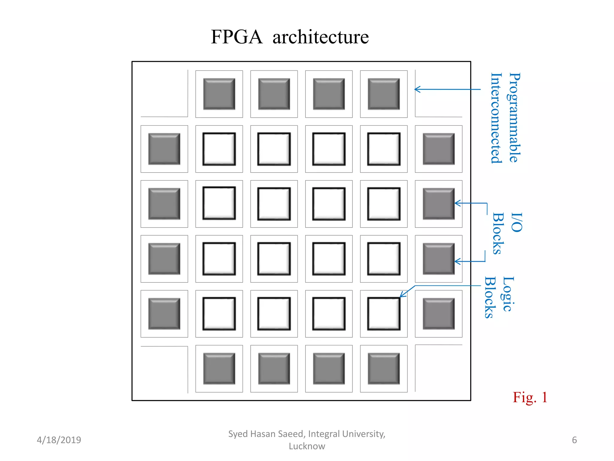
• FPGA architecture is shown in fig. 1
4/18/2019
Syed Hasan Saeed, Integral University,
Lucknow
4
ADVANTAGES:
• FPGA is fast.
• FPGA is suitable for microprocessor.
• It is suitable for parallel data processing.
• Real time applications.
• Synthesis of FPGA is easier than ASCI.FPGA are suitable choice
for DSP or microcontrollers.
DISADVANTAGES:
• FPGA is slightly costly.
• It’s program is not easier.
• FPGA are generally slower than ASIC.
• FPGA can’t handle complex design.
• It draws more power.
4/18/2019
Syed Hasan Saeed, Integral University,
Lucknow
5
4/18/2019
Syed Hasan Saeed, Integral University,
Lucknow
6
I/O
Blocks
Logic
Blocks
Programmable
Interconnected
FPGA architecture
Fig. 1

FPGA

  • 1.
    Field Programmable GateArray (FPGA) SYED HASAN SAEED hasansaeedcontrol@gmail.com https://shasansaeed.yolasite.com 4/18/2019 1 Syed Hasan Saeed, Integral University, Lucknow
  • 2.
    Field Programmable GateArray (FPGA): • FPGA is cluster of logic blocks which can be arranged by the clients. • The term ‘field programmable’ here implies that the device is programmable outside the factory where it is fabricated. • FPGA consists of I/O pins. • Every one of I/O block gives independently selectable input, output or bidirectional access to one of the general-purpose I/O pins on the FPGA package. • All logic gates are connected with each other by conducting material known as channel. • FPGA have 84 to 256 pins. • With FPGA it is possible to integrate arithmetic and logic circuits, controllers etc on the same device. 4/18/2019 Syed Hasan Saeed, Integral University, Lucknow 2
  • 3.
    • A fieldProgrammable Gate Array is a programmable logic device (PLD) with higher logic densities and capable of implementing different functions in a short period of time. • In FPGA, the programmed configuration is usually volatile and therefore needs to be reloaded whenever is applied or a different functionality is required. APPLICATIONS: • FPGA is used for Digital Signal Processing (DSP). • There are various applications of FPGA like video & image processing, data processing and storage, speech recognition, Bioinformatics, instrumentation and telecommunications, high end RADAs etc. 4/18/2019 Syed Hasan Saeed, Integral University, Lucknow 3
  • 4.
    FPGA Design andProgramming: • To defined the behavior of FPGA the user provides a hardware description language (HDL) or a schematic design. • Then, using electronic automation tool. • Technology mapped net list is generated. • The net list can then be fitted to the actual FPGA architecture using a process called place and route. • The user will validate the map, place and route result via timing analysis, simulation and other verification methodologies. • Once the design and validation process is complete, the binary file generated used to configure the FPGA. • FPGA architecture is shown in fig. 1 4/18/2019 Syed Hasan Saeed, Integral University, Lucknow 4
  • 5.
    ADVANTAGES: • FPGA isfast. • FPGA is suitable for microprocessor. • It is suitable for parallel data processing. • Real time applications. • Synthesis of FPGA is easier than ASCI.FPGA are suitable choice for DSP or microcontrollers. DISADVANTAGES: • FPGA is slightly costly. • It’s program is not easier. • FPGA are generally slower than ASIC. • FPGA can’t handle complex design. • It draws more power. 4/18/2019 Syed Hasan Saeed, Integral University, Lucknow 5
  • 6.
    4/18/2019 Syed Hasan Saeed,Integral University, Lucknow 6 I/O Blocks Logic Blocks Programmable Interconnected FPGA architecture Fig. 1