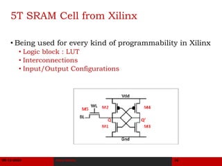
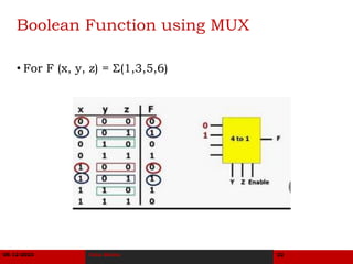
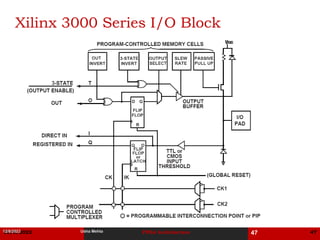
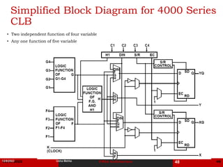
SlideShare a Scribd company logo
1 of 74
12/8/2023 FPGA Architecture 1
Field Programmable
Gate Arrays
Dr Usha Mehta
usha.mehta@nirmauni.ac.in
08-12-2023
Usha Mehta 1
12/8/2023 FPGA Architecture 2
Acknowledgement
This presentation has been summarized from various
books, papers, websites and presentations related to the
topic all over the world. I couldn’t remember where
these large pull of hints and work come from. However,
I’d like to thank all professors and scientists who
created such a good work on this emerging field.
Without those efforts in this very emerging technology,
these notes and slides can’t be finished.
08-12-2023 Usha Mehta 2
12/8/2023 FPGA Architecture 3
How Microprocessor Programming is
different from FPGA Programming?
08-12-2023 Usha Mehta 3
12/8/2023 FPGA Architecture 4
Evolution from CPLD
• Approach to building a “better” PLD is place a lot of primitive gates on a
die, and then place programmable interconnect between them:
12/8/2023 FPGA Architecture 5
Evolution
• Around 1980’s, there was a gap in digital ICs
• SPLD-CPLD : Programmable, fast design time,
flexibility in design modification but could not support
complex design
• ASIC : Could support complex design but painfully
expensive in time and cost, once the design has been
implemented, it’s frozen, no flexibility.
• To gap this bridge, Xilinx introduces FPGAs
08-12-2023 Usha Mehta 5
12/8/2023 FPGA Architecture 6
Programmability of FPGAs
• Device-wide Programmability
• The way in which device computes can be programmed
• In processor, all programmability is in sequence of
activity, the circuit block itself has fixed functionality
• Where does this programmability come from?
• Programmable Logic Block
• Programmable Input/Output
• Programmable routing/interconnect
08-12-2023 Usha Mehta 6
12/8/2023 FPGA Architecture 7
Basics of FPGA
The FPGA approach to arrange primitive logic
elements (logic cells) arrange in rows/columns with
programmable routing between them.
What constitutes a primitive logic element? Lots of
different choices can be made! Primitive element
must be classified as a “complete logic family”.
• A primitive gate like a NAND gate
• A 2/1 mux (this happens to be a complete logic
family)
• A Lookup table (I.e, 16x1 lookup table can
implement any 4 input logic function).
Often combine one of the above with a DFF to form
the primitive logic element.
12/8/2023 FPGA Architecture 8
Comparison of FPGA-ASIC-
Microprocessor
08-12-2023 Usha Mehta 8
12/8/2023 FPGA Architecture 9
FPGA’s popularity in applications like…
• Glue Logic (replace SSI and MSI parts)
• Rapid turnaround
• Prototype design
• Emulation
• Custom computing
• Dynamic reconfiguration
08-12-2023 Usha Mehta 9
12/8/2023 FPGA Architecture 10
When FPGAs are good choice?
• High speed needed (compared to Microprocessor)
• Computation can be parallelized
• Bit level operations
• Reconfigurability is important
• Small to medium size production quantity
• No strict power constraints ( compared to ASICs)
08-12-2023 Usha Mehta 10
12/8/2023 FPGA Architecture 11
Cons of FPGAs
• Power consumption (compared to ASIC)
• Long design time ( compared to microprocessor-
software)
• Silicon Area overhead
• 20 to 80% in ASIC (DFT)
• 90% in Processor (Caches etc)
• 99% in FPGA ( programmable logic and routing)
• No need to worries…. MOORE’S LAW is there….
08-12-2023 Usha Mehta 11
12/8/2023 FPGA Architecture 12
FPGA Classification
08-12-2023 Usha Mehta 12
Implementation
Architecture
Logic
Implementation
Programmable
Technology
Symmetrical Array
Row based Array
Hierarchial PLD
Sea of Gates
Look Up table
Multiplexer
based
PLD Block
NAND Gates
Static Ram
Antifuse
E/EPROM
FPGA types
12/8/2023 FPGA Architecture 13
SRAM Based FPGA : Xilinx
• Island/Cellular structure
• Volatile
• Required external memory to store
programming info / bit stream file
• Very less power
• Large area
• Easy to reconfigure
08-12-2023 Usha Mehta 13
12/8/2023 FPGA Architecture 14
EPROM Based : Altera
• Array based
• Non-volatile
• Reconfigurable ( out of circuit/ In circuit)
• High Power consumption
• Small in size
08-12-2023 Usha Mehta 14
12/8/2023 FPGA Architecture 15
Antifuse Based : Actel
• Channeled
• Non volatile
• One time programmable
• Small in size
• Less Power
08-12-2023 Usha Mehta 15
12/8/2023 FPGA Architecture 16
Island Style Xilinx FPGA
12/8/2023 Usha Mehta
16
CLB
CLB CLB
CLB CLB
CLB
Configurable
Logic
Block
IOB
IOB
IOB IOB IOB
Input
Output
Block
Programmable
Interconnect
12/8/2023 FPGA Architecture 17
SRAM for Xilinx
• Each programmable point is SRAM cell being loaded
from external source.
• This SRAM cells are written only once for each
application so no need of high speed like commercial
SRAM
• The SRAM is volatile but SRAM FPGAs include a logic
to sense power-on and to automatically initialize them
selves and reconfigure the FPGA so providing virtually-
non-volatility provided application can wait 2ms-30ms.
• Hence this FPGAs need an external memory
08-12-2023 Usha Mehta 17
12/8/2023 FPGA Architecture 18
5T SRAM Cell from Xilinx
• Being used for every kind of programmability in Xilinx
• Logic block : LUT
• Interconnections
• Input/Output Configurations
08-12-2023 Usha Mehta 18
12/8/2023 FPGA Architecture 19
Programmability in
Logic
08-12-2023
Usha Mehta 19
12/8/2023 FPGA Architecture 20
:Primitive Gates / Universal Gates
• PAL and PLA use the SOP form and hence use INV,
AND and OR arrays.
• The gate requirements vary with functions.
• Example: For a 4 variable functions, there are 224
possible functions and each require the different no of
AND and OR gates.
• Even if we implement the functions using NAND/ NOR
gates (Universal gates), the requirement of no. of gates
varies with function.
08-12-2023 Usha Mehta 20
12/8/2023 FPGA Architecture 21
Multiplexer
• Any Boolean function can be implemented using 2:1
MUX.
• If 8 variable function is to be implemented using single
MUX, what can be the size of MUX?
08-12-2023 Usha Mehta 21
12/8/2023 FPGA Architecture 22
Boolean Function using MUX
• For F (x, y, z) = Σ(1,3,5,6)
08-12-2023 Usha Mehta 22
12/8/2023 FPGA Architecture 23
Lookup Table
08-12-2023 Usha Mehta 23
SRAM
12/8/2023 FPGA Architecture 24
LUT using 2:1 MUX
08-12-2023 Usha Mehta 24
12/8/2023 FPGA Architecture 25
Example 2 Input LUT
12/8/2023 Usha Mehta 25
x1 x2 f
0 0 1
0 1 0
1 0 0
1 1 1
f = x1'x2' + x1x2, or using Shannon's expansion:
f = x1'(x2') + x1(x2)
= x1'(x2'(1) + x2(0)) + x1(x2'(0) + x2(1))
f
1
0
0
1
x1
x2
12/8/2023 FPGA Architecture 26
3 Input LUT
12/8/2023 Usha Mehta 26
– 7 2x1 MUXes and
8 storage cells are
required
– Commercial LUTs have
4-5 inputs, and 16-32
storage cells
f
0/1
0/1
0/1
0/1
0/1
0/1
0/1
0/1
x2
x3
x1
12/8/2023 FPGA Architecture 27
LUT using Transmission Gate
08-12-2023 Usha Mehta 27
12/8/2023 FPGA Architecture 28
Out
D Q
Clock
Select
Flip-flop
In
1
In
2
In
3
LUT
Se logic block = LUT + Flipflop
12/8/2023 Usha Mehta
28
12/8/2023 FPGA Architecture 29
Fine Grained FPGAs
• Fine Grained: Small Unit like NAND gates, LUTs,
MUXes only…..
• When complex building blocks / Units are also present
in CLB, then it is called Coarse Grained FPGA.
08-12-2023 Usha Mehta 29
12/8/2023 FPGA Architecture 30
Programmability in
Interconnections
08-12-2023
Usha Mehta 30
12/8/2023 FPGA Architecture 31
Routing
• Routing contains 80-90% of FPGA total area
• Mesh based routing network
• Logic blocks are connected to the routing network through
connection
boxes (CB).
• Horizontal and vertical routing tracks which are interconnected
through switch
boxes (SB).
08-12-2023 Usha Mehta 31
12/8/2023 FPGA Architecture 32
Routing
08-12-2023 Usha Mehta 32
12/8/2023 FPGA Architecture 33
Flexibility in Routing
• FC=Flexibility of Connection
Box
= the number of routing
tracks
of adjacent channel which
are connected to the pin of a
block
• FS=Flexibility of Switch Box
=the total number of tracks
with which every track
entering in the switch box
connects to
08-12-2023 Usha Mehta 33
12/8/2023 FPGA Architecture 34
Routing Switch and Connection Switch
• The output pins of a block can connect to any routing
track through pass transistors.
• The pass transistor forms a tristate output that can be
independently turned on or off
08-12-2023 Usha Mehta 34
12/8/2023 FPGA Architecture 35
Programmable Interconnect Point (PIP)
Configurable Interconnect Point (CIP)
08-12-2023 Usha Mehta 35
12/8/2023 FPGA Architecture 36
Programmable Interconnection Points
PIPs
12/8/2023 Usha Mehta
36
programmable switch element
turning the corner, etc.
12/8/2023 FPGA Architecture 37
Use of Multiplexer instead of Pass Gate
08-12-2023 Usha Mehta 37
12/8/2023 FPGA Architecture 38
Single-Driver Directional Routing
• No use of tristate elements.
• The output of block needs to be connected to the
neighboring routing network through multiplexors in
the switch box.
08-12-2023 Usha Mehta 38
12/8/2023 FPGA Architecture 39
08-12-2023 Usha Mehta 39
12/8/2023 FPGA Architecture 40
Types of Interconnect
• General Purpose
• Direct Between Adjacent Cell
• Vertical and Horizontal Long Lines
08-12-2023 Usha Mehta 40
12/8/2023 FPGA Architecture 41
Short and Long Wire Segments
08-12-2023 Usha Mehta 41
12/8/2023 FPGA Architecture 42
Programmability in
Input-Output
08-12-2023
Usha Mehta 42
12/8/2023 FPGA Architecture 43
Programmable IOB
08-12-2023 Usha Mehta 43
12/8/2023 FPGA Architecture 44
Nomenclature
12/8/2023 Usha Mehta
44
12/8/2023 FPGA Architecture 45
Xilinx 3000 Series Logic Cell
12/8/2023 Usha Mehta
45
12/8/2023 FPGA Architecture 46
Combinational Logic Options
12/8/2023 Usha Mehta
46
12/8/2023 FPGA Architecture 47
Xilinx 3000 Series I/O Block
12/8/2023 Usha Mehta
47
12/8/2023 FPGA Architecture 48
Simplified Block Diagram for 4000 Series
CLB
• Two independent function of four variable
• Any one function of five variable
12/8/2023 Usha Mehta
48
12/8/2023 FPGA Architecture 49
Realization of Six variable Function –
12/8/2023 Usha Mehta
49
12/8/2023 FPGA Architecture 50
Realization of Seven Variable
Function…..
12/8/2023 Usha Mehta
50
12/8/2023 FPGA Architecture 51
Fine Grained FPGA
&
Coarse Grained FPGA
08-12-2023
Usha Mehta 51
12/8/2023 FPGA Architecture 52
Fine Grained FPGA
• Fine Grained: Small Unit like NAND gates,
LUTs, MUXes only…..
• Gate-Array: regular structure of “logic cells”,
connected through an interconnection
network
• Configuration stored in SRAM, must be
loaded on startup
EPROM
12/8/2023 FPGA Architecture 53
Limitation of Fine Grained FPGA
• If you wanted to do floating point math with a fine
grained LUT2 FPGA, that would not be as efficient and
will have hardware limitations
• What is such complex units are already fabricated in
FPGA as std. cell?
• coarse grained FPGA has floating point, or even
integer, adders, barrel shifters, and or PLA elements in
them that can be cascaded for larger bit words. that
would make a fast adder and take less area than fine
grained and utilize closer to 100% of the complex logic
block.
08-12-2023 Usha Mehta 53
12/8/2023 FPGA Architecture 54
Coarse Grained FPGA
• Higher level logic blocks as unit
• Embedded memory
• Many hardware applications need
memory for data storage. Many
FPGAs include blocks of RAM for
this purpose
• Dedicated logic for carry
generation, or other arithmetic
functions
• Phase locked loops for clock
synchronization, division,
multiplication
08-12-2023 Usha Mehta 54
I/O Buffer
PLB
Embedded RAM IP Core
Routing
12/8/2023 FPGA Architecture 55
Platform FPGA
• It contains
• CPUs
• Embedded memory
• Memory interface
• High-speed serial I/O standard
• Bus interfaces
• Altera Stratix: Memory blocks + DSP
08-12-2023 Usha Mehta 55
12/8/2023 FPGA Architecture 56
Processor in FPGAs
• Softcore microprocessor:
• using FPGA resources only
• Synthesize and compiling need: tools are very important
• Xilinx offering: MicroBlaze & PicoBlaze
• Altera offering: NIOS
• Hardcore microprocessor:
• hardwired in FPGA architecture
• 3rd party tools
• Xilinx: (Virtex II Pro) PowerPC from IBM
• Altera: (Excalibur APEX) ARM922T from ARM
08-12-2023 Usha Mehta 56
12/8/2023 FPGA Architecture 57
Soft Core Processor
• Soft-core Processor
• HDL description
• Flexible implementation
• FPGA or ASIC
• Technology independent
• A soft processor is very
configurable
• How to optimize the
implementation without too
many variants?
• Avoid too much low-level and
only do it when necessary
• MicroBlaze is a mixture of
very detailed implementation
and pure RTL code
08-12-2023 Usha Mehta 57
HDL
Description
FPGA ASIC
Spartan 3 Virtex 2 Virtex 4
12/8/2023 FPGA Architecture 58
Use of Volatile/Reprogrammability
• At board level test
• As part of test sequence, the FPGA on board is
configured as test generator/checker and after test is
finished, it is reconfigured with regular application
logic.
• Reduces the additional hardware requirement for the
test
08-12-2023 Usha Mehta 58
12/8/2023 FPGA Architecture 59
FPGA Soft Core Processors
• Soft Core Processors can have configurable options
• Datapath units
• Cache
• Bus architecture
• Current commercial FPGA Soft-Core Processors
• Xilinx Microblaze
• Altera Nios
08-12-2023 Usha Mehta 59
12/8/2023 FPGA Architecture 60
Multi-FPGA System
• Designed for an individual application
• When design is to big or to prototype a new custom
design
• Emulators
• Dynamically reconfigurable systems
• Partitioning and routing is an issue
08-12-2023 Usha Mehta 60
12/8/2023 FPGA Architecture 61
Design Flow
08-12-2023 Usha Mehta 61
ASIC FPGA
12/8/2023 FPGA Architecture 62
Comparing with ASICs
• The dramatic increase in ASIC design costs have had a real effect on the ASIC
market, reducing the number of new designs and dramatically reducing the
number of vendors serving the ASIC market.
12/8/2023 Usha Mehta 62
12/8/2023 FPGA Architecture 63
Does it mean ASIC is over?
• One would expect that such a trend would have a very positive effect on
the FPGA market. This is because there is no mask-set cost associated
with an FPGA design and, accordingly, far lower NRE costs per design.
• “In 2010 there were 2,500 ASIC design starts versus 90,000 FPGA design
starts.” !!!!!!
12/8/2023 Usha Mehta 63
12/8/2023 FPGA Architecture 64
Is this reality?
12/8/2023 Usha Mehta 64
12/8/2023 FPGA Architecture 65
Current Scenario of Design Starts per
Node
• One can easily see that the most popular current design node is at 180nm.
Clearly, even such an old node provides a better product than the state-of-
the art FPGA. A 65nm Standard Cell design to an FPGA of 28nm suggests
that far more designs could be better off with Standard Cell.
12/8/2023 FPGA Architecture 66
12/8/2023 FPGA Architecture 67
CMOS Logic Market Share
earlier in 2004
Std logic
Programmable
GA
Std cell
Custom
Chipset
Std logic
Programmable
GA
Std cell
Custom
Chipset
Source:dataquest
10%
9%
29%
30%
8%
14%
12/8/2023 FPGA Architecture 68
CMOS PLD Market Share
earlier in 2004
Other
Cpress
AT&T
Actel
Lattice
AMD
Altera
Xilinx
Source:dataquest
5%
3%
5%
6%
11%
15%
24%
31%
12/8/2023 FPGA Architecture 69
Current Scenario of Design Starts per
Node
• One can easily see that the most popular current design node is at 180nm. Clearly,
even such an old node provides a better product than the state-of-the art FPGA.
12/8/2023 FPGA Architecture 70
What stops FPGA to grow drastically?
• A 2007 research paper by Ian Kuon and Prof Jonathan Rose (IEEE Transaction on
Computer-Aided Design of IC and System) says this clearly: "In this paper, we have
presented empirical measurements quantifying the gap between FPGAs and ASICs for
core logic. We found that for circuits implemented purely using the LUT based logic
elements, an FPGA is approximately 35 times larger and between 3.4 to 4.6 times slower
on average than a standard-cell implementation."
12/8/2023 Usha Mehta 70
12/8/2023 FPGA Architecture 71
FPGA (Lookup-Table) vs. ASIC (Static
CMOS Gate)
• For CMOS gate, # of transistors depends on
function and # of inputs.
• In SRAM cell, it is fixed. 1 cell requires nearly six
transistors.
• For NAND4 will require 8 transistors. For four
input function in SRAM, 4 X 8 =32 transistors will
be used. In addition to this, it will require
decoder/MUX. How many transistors required for
a mux used to decode the lookup table of 4 bit?
• Delay in CMOS depends on function and # of
inputs but in SRAM, it is always fixed and greater
than CMOS.
• Power in CMOS is only during transition while in
SRAM, it is continuous.
12/8/2023 Usha Mehta
71
12/8/2023 FPGA Architecture 72
"Few engineers will design custom chips;
Some engineers will design ASIC and SoCs;
Many engineers will design FPGA systems”
Then how you may differentiate yourself from
those many engineers ?
Of course, by thorough , detailed knowledge of
FPGA starting with PLDs.
12/8/2023 Usha Mehta 72
12/8/2023 FPGA Architecture 73
A Maturing Market
• Dominated by two players, Xilinx and Altera
• With 51% and 32% share = 83% combined
• Remaining players scramble for niches
• All non-dedicated players have given up:
• Intel, T.I., Motorola, NSC, AMD, Cypress, Philips…
• Late-comers have been absorbed or failed:
• Dynachip, PlusLogic, Triscend, SiliconSpice (absorbed)
Chameleon, Quicksilver, Morphics, Adaptive Silicon (failed)
The pace of innovation is set by the leaders
12/8/2023 Usha Mehta
73
12/8/2023 FPGA Architecture 74
Thank you!
08-12-2023 Usha Mehta 74

More Related Content

What's hot

Sta by usha_mehta
Sta by usha_mehtaSta by usha_mehta
Sta by usha_mehtaUsha Mehta
 
2_DVD_ASIC_Design_FLow.pdf
2_DVD_ASIC_Design_FLow.pdf2_DVD_ASIC_Design_FLow.pdf
2_DVD_ASIC_Design_FLow.pdfUsha Mehta
 
2019 3 testing and verification of vlsi design_sta
2019 3 testing and verification of vlsi design_sta2019 3 testing and verification of vlsi design_sta
2019 3 testing and verification of vlsi design_staUsha Mehta
 
10 static timing_analysis_1_concept_of_timing_analysis
10 static timing_analysis_1_concept_of_timing_analysis10 static timing_analysis_1_concept_of_timing_analysis
10 static timing_analysis_1_concept_of_timing_analysisUsha Mehta
 
Power Reduction Techniques
Power Reduction TechniquesPower Reduction Techniques
Power Reduction TechniquesRajesh M
 
Vlsi physical design automation on partitioning
Vlsi physical design automation on partitioningVlsi physical design automation on partitioning
Vlsi physical design automation on partitioningSushil Kundu
 
Timing closure document
Timing closure documentTiming closure document
Timing closure documentAlan Tran
 
Physical design
Physical design Physical design
Physical design Mantra VLSI
 
12 static timing_analysis_3_clocked_design
12 static timing_analysis_3_clocked_design12 static timing_analysis_3_clocked_design
12 static timing_analysis_3_clocked_designUsha Mehta
 
VLSI-Physical Design- Tool Terminalogy
VLSI-Physical Design- Tool TerminalogyVLSI-Physical Design- Tool Terminalogy
VLSI-Physical Design- Tool TerminalogyMurali Rai
 
4 verification flow_planning
4 verification flow_planning4 verification flow_planning
4 verification flow_planningUsha Mehta
 
sta slide ref.pdf
sta slide ref.pdfsta slide ref.pdf
sta slide ref.pdfquandao25
 
Static_Timing_Analysis_in_detail.pdf
Static_Timing_Analysis_in_detail.pdfStatic_Timing_Analysis_in_detail.pdf
Static_Timing_Analysis_in_detail.pdfUsha Mehta
 
Placement in VLSI Design
Placement in VLSI DesignPlacement in VLSI Design
Placement in VLSI DesignTeam-VLSI-ITMU
 

What's hot (20)

Sta by usha_mehta
Sta by usha_mehtaSta by usha_mehta
Sta by usha_mehta
 
2_DVD_ASIC_Design_FLow.pdf
2_DVD_ASIC_Design_FLow.pdf2_DVD_ASIC_Design_FLow.pdf
2_DVD_ASIC_Design_FLow.pdf
 
Power Gating
Power GatingPower Gating
Power Gating
 
2019 3 testing and verification of vlsi design_sta
2019 3 testing and verification of vlsi design_sta2019 3 testing and verification of vlsi design_sta
2019 3 testing and verification of vlsi design_sta
 
10 static timing_analysis_1_concept_of_timing_analysis
10 static timing_analysis_1_concept_of_timing_analysis10 static timing_analysis_1_concept_of_timing_analysis
10 static timing_analysis_1_concept_of_timing_analysis
 
Power Reduction Techniques
Power Reduction TechniquesPower Reduction Techniques
Power Reduction Techniques
 
Floor plan & Power Plan
Floor plan & Power Plan Floor plan & Power Plan
Floor plan & Power Plan
 
Vlsi physical design automation on partitioning
Vlsi physical design automation on partitioningVlsi physical design automation on partitioning
Vlsi physical design automation on partitioning
 
Static_Time_Analysis.pptx
Static_Time_Analysis.pptxStatic_Time_Analysis.pptx
Static_Time_Analysis.pptx
 
Powerplanning
PowerplanningPowerplanning
Powerplanning
 
Timing closure document
Timing closure documentTiming closure document
Timing closure document
 
Eco
EcoEco
Eco
 
Physical design
Physical design Physical design
Physical design
 
Physical design
Physical design Physical design
Physical design
 
12 static timing_analysis_3_clocked_design
12 static timing_analysis_3_clocked_design12 static timing_analysis_3_clocked_design
12 static timing_analysis_3_clocked_design
 
VLSI-Physical Design- Tool Terminalogy
VLSI-Physical Design- Tool TerminalogyVLSI-Physical Design- Tool Terminalogy
VLSI-Physical Design- Tool Terminalogy
 
4 verification flow_planning
4 verification flow_planning4 verification flow_planning
4 verification flow_planning
 
sta slide ref.pdf
sta slide ref.pdfsta slide ref.pdf
sta slide ref.pdf
 
Static_Timing_Analysis_in_detail.pdf
Static_Timing_Analysis_in_detail.pdfStatic_Timing_Analysis_in_detail.pdf
Static_Timing_Analysis_in_detail.pdf
 
Placement in VLSI Design
Placement in VLSI DesignPlacement in VLSI Design
Placement in VLSI Design
 

Similar to Field Programmable Gate Arrays : Architecture

1.FPGA for dummies: Basic FPGA architecture
1.FPGA for dummies: Basic FPGA architecture 1.FPGA for dummies: Basic FPGA architecture
1.FPGA for dummies: Basic FPGA architecture Maurizio Donna
 
lecture25_fpga-conclude.ppt
lecture25_fpga-conclude.pptlecture25_fpga-conclude.ppt
lecture25_fpga-conclude.pptSourav Roy
 
2.FPGA for dummies: modern FPGA architecture
2.FPGA for dummies: modern FPGA architecture2.FPGA for dummies: modern FPGA architecture
2.FPGA for dummies: modern FPGA architectureMaurizio Donna
 
FPGA vs Microcontroller - Which one is Best for Embedded Application_.pdf
FPGA vs Microcontroller - Which one is Best for Embedded Application_.pdfFPGA vs Microcontroller - Which one is Best for Embedded Application_.pdf
FPGA vs Microcontroller - Which one is Best for Embedded Application_.pdfaud Scarlet
 
Lecture Slide (1).pptx
Lecture Slide (1).pptxLecture Slide (1).pptx
Lecture Slide (1).pptxBilalMumtaz9
 
Field programmable Gate Arrays Chapter 6.pdf
Field programmable Gate Arrays Chapter 6.pdfField programmable Gate Arrays Chapter 6.pdf
Field programmable Gate Arrays Chapter 6.pdfffwwx10
 
Automatic generation of platform architectures using open cl and fpga roadmap
Automatic generation of platform architectures using open cl and fpga roadmapAutomatic generation of platform architectures using open cl and fpga roadmap
Automatic generation of platform architectures using open cl and fpga roadmapManolis Vavalis
 
Field programable gate array
Field programable gate arrayField programable gate array
Field programable gate arrayNeha Agarwal
 
FPGA in outer space seminar report
FPGA in outer space seminar reportFPGA in outer space seminar report
FPGA in outer space seminar reportrahul kumar verma
 
A Primer on FPGAs - Field Programmable Gate Arrays
A Primer on FPGAs - Field Programmable Gate ArraysA Primer on FPGAs - Field Programmable Gate Arrays
A Primer on FPGAs - Field Programmable Gate ArraysTaylor Riggan
 
programmable_devices_en_02_2014
programmable_devices_en_02_2014programmable_devices_en_02_2014
programmable_devices_en_02_2014Svetozar Jovanovic
 
Introduction to FPGA.pdf
Introduction to FPGA.pdfIntroduction to FPGA.pdf
Introduction to FPGA.pdfghazi21
 
VLSI design Dr B.jagadeesh UNIT-5.pptx
VLSI design Dr B.jagadeesh   UNIT-5.pptxVLSI design Dr B.jagadeesh   UNIT-5.pptx
VLSI design Dr B.jagadeesh UNIT-5.pptxjagadeesh276791
 

Similar to Field Programmable Gate Arrays : Architecture (20)

VLSI PLDS pla, pal
VLSI PLDS pla, palVLSI PLDS pla, pal
VLSI PLDS pla, pal
 
1.FPGA for dummies: Basic FPGA architecture
1.FPGA for dummies: Basic FPGA architecture 1.FPGA for dummies: Basic FPGA architecture
1.FPGA for dummies: Basic FPGA architecture
 
lecture25_fpga-conclude.ppt
lecture25_fpga-conclude.pptlecture25_fpga-conclude.ppt
lecture25_fpga-conclude.ppt
 
2.FPGA for dummies: modern FPGA architecture
2.FPGA for dummies: modern FPGA architecture2.FPGA for dummies: modern FPGA architecture
2.FPGA for dummies: modern FPGA architecture
 
FPGA vs Microcontroller - Which one is Best for Embedded Application_.pdf
FPGA vs Microcontroller - Which one is Best for Embedded Application_.pdfFPGA vs Microcontroller - Which one is Best for Embedded Application_.pdf
FPGA vs Microcontroller - Which one is Best for Embedded Application_.pdf
 
FPGA In a Nutshell
FPGA In a NutshellFPGA In a Nutshell
FPGA In a Nutshell
 
lecture25_fpga-conclude.ppt
lecture25_fpga-conclude.pptlecture25_fpga-conclude.ppt
lecture25_fpga-conclude.ppt
 
Lecture Slide (1).pptx
Lecture Slide (1).pptxLecture Slide (1).pptx
Lecture Slide (1).pptx
 
Dr.D.RUKMANIDEVI PPT.ppt
Dr.D.RUKMANIDEVI PPT.pptDr.D.RUKMANIDEVI PPT.ppt
Dr.D.RUKMANIDEVI PPT.ppt
 
Field programmable Gate Arrays Chapter 6.pdf
Field programmable Gate Arrays Chapter 6.pdfField programmable Gate Arrays Chapter 6.pdf
Field programmable Gate Arrays Chapter 6.pdf
 
Automatic generation of platform architectures using open cl and fpga roadmap
Automatic generation of platform architectures using open cl and fpga roadmapAutomatic generation of platform architectures using open cl and fpga roadmap
Automatic generation of platform architectures using open cl and fpga roadmap
 
FIELD PROGRAMMABLE GATE ARRAYS AND THEIR APPLICATIONS
FIELD PROGRAMMABLE GATE ARRAYS AND THEIR APPLICATIONSFIELD PROGRAMMABLE GATE ARRAYS AND THEIR APPLICATIONS
FIELD PROGRAMMABLE GATE ARRAYS AND THEIR APPLICATIONS
 
Field programable gate array
Field programable gate arrayField programable gate array
Field programable gate array
 
FPGA in outer space seminar report
FPGA in outer space seminar reportFPGA in outer space seminar report
FPGA in outer space seminar report
 
A Primer on FPGAs - Field Programmable Gate Arrays
A Primer on FPGAs - Field Programmable Gate ArraysA Primer on FPGAs - Field Programmable Gate Arrays
A Primer on FPGAs - Field Programmable Gate Arrays
 
programmable_devices_en_02_2014
programmable_devices_en_02_2014programmable_devices_en_02_2014
programmable_devices_en_02_2014
 
Introduction to FPGA.pdf
Introduction to FPGA.pdfIntroduction to FPGA.pdf
Introduction to FPGA.pdf
 
VLSI design Dr B.jagadeesh UNIT-5.pptx
VLSI design Dr B.jagadeesh   UNIT-5.pptxVLSI design Dr B.jagadeesh   UNIT-5.pptx
VLSI design Dr B.jagadeesh UNIT-5.pptx
 
FPGA
FPGAFPGA
FPGA
 
3rd Lecture
3rd Lecture3rd Lecture
3rd Lecture
 

More from Usha Mehta

Basic Design Flow for Field Programmable Gate Arrays
Basic Design Flow for Field Programmable Gate ArraysBasic Design Flow for Field Programmable Gate Arrays
Basic Design Flow for Field Programmable Gate ArraysUsha Mehta
 
5_DVD_VLSI Technology Trends.pdf
5_DVD_VLSI Technology Trends.pdf5_DVD_VLSI Technology Trends.pdf
5_DVD_VLSI Technology Trends.pdfUsha Mehta
 
13_DVD_Latch-up_prevention.pdf
13_DVD_Latch-up_prevention.pdf13_DVD_Latch-up_prevention.pdf
13_DVD_Latch-up_prevention.pdfUsha Mehta
 
14 static timing_analysis_5_clock_domain_crossing
14 static timing_analysis_5_clock_domain_crossing14 static timing_analysis_5_clock_domain_crossing
14 static timing_analysis_5_clock_domain_crossingUsha Mehta
 
9 semiconductor memory
9 semiconductor memory9 semiconductor memory
9 semiconductor memoryUsha Mehta
 
11 static timing_analysis_2_combinational_design
11 static timing_analysis_2_combinational_design11 static timing_analysis_2_combinational_design
11 static timing_analysis_2_combinational_designUsha Mehta
 
6 verification tools
6 verification tools6 verification tools
6 verification toolsUsha Mehta
 
5 verification methods
5 verification methods5 verification methods
5 verification methodsUsha Mehta
 
3 test economic_test_equipments_yield
3 test economic_test_equipments_yield3 test economic_test_equipments_yield
3 test economic_test_equipments_yieldUsha Mehta
 
2 when to_test_role_of_testing
2 when to_test_role_of_testing2 when to_test_role_of_testing
2 when to_test_role_of_testingUsha Mehta
 
Verification flow and_planning_vlsi_design
Verification flow and_planning_vlsi_designVerification flow and_planning_vlsi_design
Verification flow and_planning_vlsi_designUsha Mehta
 
Introduction of testing and verification of vlsi design
Introduction of testing and verification of vlsi designIntroduction of testing and verification of vlsi design
Introduction of testing and verification of vlsi designUsha Mehta
 
BUilt-In-Self-Test for VLSI Design
BUilt-In-Self-Test for VLSI DesignBUilt-In-Self-Test for VLSI Design
BUilt-In-Self-Test for VLSI DesignUsha Mehta
 
Design-for-Test (Testing of VLSI Design)
Design-for-Test (Testing of VLSI Design)Design-for-Test (Testing of VLSI Design)
Design-for-Test (Testing of VLSI Design)Usha Mehta
 
Automatic Test Pattern Generation (Testing of VLSI Design)
Automatic Test Pattern Generation (Testing of VLSI Design)Automatic Test Pattern Generation (Testing of VLSI Design)
Automatic Test Pattern Generation (Testing of VLSI Design)Usha Mehta
 

More from Usha Mehta (17)

Basic Design Flow for Field Programmable Gate Arrays
Basic Design Flow for Field Programmable Gate ArraysBasic Design Flow for Field Programmable Gate Arrays
Basic Design Flow for Field Programmable Gate Arrays
 
5_DVD_VLSI Technology Trends.pdf
5_DVD_VLSI Technology Trends.pdf5_DVD_VLSI Technology Trends.pdf
5_DVD_VLSI Technology Trends.pdf
 
13_DVD_Latch-up_prevention.pdf
13_DVD_Latch-up_prevention.pdf13_DVD_Latch-up_prevention.pdf
13_DVD_Latch-up_prevention.pdf
 
14 static timing_analysis_5_clock_domain_crossing
14 static timing_analysis_5_clock_domain_crossing14 static timing_analysis_5_clock_domain_crossing
14 static timing_analysis_5_clock_domain_crossing
 
9 semiconductor memory
9 semiconductor memory9 semiconductor memory
9 semiconductor memory
 
11 static timing_analysis_2_combinational_design
11 static timing_analysis_2_combinational_design11 static timing_analysis_2_combinational_design
11 static timing_analysis_2_combinational_design
 
6 verification tools
6 verification tools6 verification tools
6 verification tools
 
5 verification methods
5 verification methods5 verification methods
5 verification methods
 
3 test economic_test_equipments_yield
3 test economic_test_equipments_yield3 test economic_test_equipments_yield
3 test economic_test_equipments_yield
 
2 when to_test_role_of_testing
2 when to_test_role_of_testing2 when to_test_role_of_testing
2 when to_test_role_of_testing
 
1 why to_test
1 why to_test1 why to_test
1 why to_test
 
1 why to_test
1 why to_test1 why to_test
1 why to_test
 
Verification flow and_planning_vlsi_design
Verification flow and_planning_vlsi_designVerification flow and_planning_vlsi_design
Verification flow and_planning_vlsi_design
 
Introduction of testing and verification of vlsi design
Introduction of testing and verification of vlsi designIntroduction of testing and verification of vlsi design
Introduction of testing and verification of vlsi design
 
BUilt-In-Self-Test for VLSI Design
BUilt-In-Self-Test for VLSI DesignBUilt-In-Self-Test for VLSI Design
BUilt-In-Self-Test for VLSI Design
 
Design-for-Test (Testing of VLSI Design)
Design-for-Test (Testing of VLSI Design)Design-for-Test (Testing of VLSI Design)
Design-for-Test (Testing of VLSI Design)
 
Automatic Test Pattern Generation (Testing of VLSI Design)
Automatic Test Pattern Generation (Testing of VLSI Design)Automatic Test Pattern Generation (Testing of VLSI Design)
Automatic Test Pattern Generation (Testing of VLSI Design)
 

Recently uploaded

result management system report for college project
result management system report for college projectresult management system report for college project
result management system report for college projectTonystark477637
 
Structural Analysis and Design of Foundations: A Comprehensive Handbook for S...
Structural Analysis and Design of Foundations: A Comprehensive Handbook for S...Structural Analysis and Design of Foundations: A Comprehensive Handbook for S...
Structural Analysis and Design of Foundations: A Comprehensive Handbook for S...Dr.Costas Sachpazis
 
Call Girls Pimpri Chinchwad Call Me 7737669865 Budget Friendly No Advance Boo...
Call Girls Pimpri Chinchwad Call Me 7737669865 Budget Friendly No Advance Boo...Call Girls Pimpri Chinchwad Call Me 7737669865 Budget Friendly No Advance Boo...
Call Girls Pimpri Chinchwad Call Me 7737669865 Budget Friendly No Advance Boo...roncy bisnoi
 
Booking open Available Pune Call Girls Koregaon Park 6297143586 Call Hot Ind...
Booking open Available Pune Call Girls Koregaon Park  6297143586 Call Hot Ind...Booking open Available Pune Call Girls Koregaon Park  6297143586 Call Hot Ind...
Booking open Available Pune Call Girls Koregaon Park 6297143586 Call Hot Ind...Call Girls in Nagpur High Profile
 
Processing & Properties of Floor and Wall Tiles.pptx
Processing & Properties of Floor and Wall Tiles.pptxProcessing & Properties of Floor and Wall Tiles.pptx
Processing & Properties of Floor and Wall Tiles.pptxpranjaldaimarysona
 
The Most Attractive Pune Call Girls Manchar 8250192130 Will You Miss This Cha...
The Most Attractive Pune Call Girls Manchar 8250192130 Will You Miss This Cha...The Most Attractive Pune Call Girls Manchar 8250192130 Will You Miss This Cha...
The Most Attractive Pune Call Girls Manchar 8250192130 Will You Miss This Cha...ranjana rawat
 
KubeKraft presentation @CloudNativeHooghly
KubeKraft presentation @CloudNativeHooghlyKubeKraft presentation @CloudNativeHooghly
KubeKraft presentation @CloudNativeHooghlysanyuktamishra911
 
Java Programming :Event Handling(Types of Events)
Java Programming :Event Handling(Types of Events)Java Programming :Event Handling(Types of Events)
Java Programming :Event Handling(Types of Events)simmis5
 
APPLICATIONS-AC/DC DRIVES-OPERATING CHARACTERISTICS
APPLICATIONS-AC/DC DRIVES-OPERATING CHARACTERISTICSAPPLICATIONS-AC/DC DRIVES-OPERATING CHARACTERISTICS
APPLICATIONS-AC/DC DRIVES-OPERATING CHARACTERISTICSKurinjimalarL3
 
(RIA) Call Girls Bhosari ( 7001035870 ) HI-Fi Pune Escorts Service
(RIA) Call Girls Bhosari ( 7001035870 ) HI-Fi Pune Escorts Service(RIA) Call Girls Bhosari ( 7001035870 ) HI-Fi Pune Escorts Service
(RIA) Call Girls Bhosari ( 7001035870 ) HI-Fi Pune Escorts Serviceranjana rawat
 
CCS335 _ Neural Networks and Deep Learning Laboratory_Lab Complete Record
CCS335 _ Neural Networks and Deep Learning Laboratory_Lab Complete RecordCCS335 _ Neural Networks and Deep Learning Laboratory_Lab Complete Record
CCS335 _ Neural Networks and Deep Learning Laboratory_Lab Complete RecordAsst.prof M.Gokilavani
 
Call Girls Service Nashik Vaishnavi 7001305949 Independent Escort Service Nashik
Call Girls Service Nashik Vaishnavi 7001305949 Independent Escort Service NashikCall Girls Service Nashik Vaishnavi 7001305949 Independent Escort Service Nashik
Call Girls Service Nashik Vaishnavi 7001305949 Independent Escort Service NashikCall Girls in Nagpur High Profile
 
(ANJALI) Dange Chowk Call Girls Just Call 7001035870 [ Cash on Delivery ] Pun...
(ANJALI) Dange Chowk Call Girls Just Call 7001035870 [ Cash on Delivery ] Pun...(ANJALI) Dange Chowk Call Girls Just Call 7001035870 [ Cash on Delivery ] Pun...
(ANJALI) Dange Chowk Call Girls Just Call 7001035870 [ Cash on Delivery ] Pun...ranjana rawat
 
OSVC_Meta-Data based Simulation Automation to overcome Verification Challenge...
OSVC_Meta-Data based Simulation Automation to overcome Verification Challenge...OSVC_Meta-Data based Simulation Automation to overcome Verification Challenge...
OSVC_Meta-Data based Simulation Automation to overcome Verification Challenge...Soham Mondal
 
UNIT-III FMM. DIMENSIONAL ANALYSIS
UNIT-III FMM.        DIMENSIONAL ANALYSISUNIT-III FMM.        DIMENSIONAL ANALYSIS
UNIT-III FMM. DIMENSIONAL ANALYSISrknatarajan
 
MANUFACTURING PROCESS-II UNIT-2 LATHE MACHINE
MANUFACTURING PROCESS-II UNIT-2 LATHE MACHINEMANUFACTURING PROCESS-II UNIT-2 LATHE MACHINE
MANUFACTURING PROCESS-II UNIT-2 LATHE MACHINESIVASHANKAR N
 
Call for Papers - African Journal of Biological Sciences, E-ISSN: 2663-2187, ...
Call for Papers - African Journal of Biological Sciences, E-ISSN: 2663-2187, ...Call for Papers - African Journal of Biological Sciences, E-ISSN: 2663-2187, ...
Call for Papers - African Journal of Biological Sciences, E-ISSN: 2663-2187, ...Christo Ananth
 
High Profile Call Girls Nagpur Isha Call 7001035870 Meet With Nagpur Escorts
High Profile Call Girls Nagpur Isha Call 7001035870 Meet With Nagpur EscortsHigh Profile Call Girls Nagpur Isha Call 7001035870 Meet With Nagpur Escorts
High Profile Call Girls Nagpur Isha Call 7001035870 Meet With Nagpur Escortsranjana rawat
 

Recently uploaded (20)

result management system report for college project
result management system report for college projectresult management system report for college project
result management system report for college project
 
DJARUM4D - SLOT GACOR ONLINE | SLOT DEMO ONLINE
DJARUM4D - SLOT GACOR ONLINE | SLOT DEMO ONLINEDJARUM4D - SLOT GACOR ONLINE | SLOT DEMO ONLINE
DJARUM4D - SLOT GACOR ONLINE | SLOT DEMO ONLINE
 
Structural Analysis and Design of Foundations: A Comprehensive Handbook for S...
Structural Analysis and Design of Foundations: A Comprehensive Handbook for S...Structural Analysis and Design of Foundations: A Comprehensive Handbook for S...
Structural Analysis and Design of Foundations: A Comprehensive Handbook for S...
 
Call Girls Pimpri Chinchwad Call Me 7737669865 Budget Friendly No Advance Boo...
Call Girls Pimpri Chinchwad Call Me 7737669865 Budget Friendly No Advance Boo...Call Girls Pimpri Chinchwad Call Me 7737669865 Budget Friendly No Advance Boo...
Call Girls Pimpri Chinchwad Call Me 7737669865 Budget Friendly No Advance Boo...
 
Booking open Available Pune Call Girls Koregaon Park 6297143586 Call Hot Ind...
Booking open Available Pune Call Girls Koregaon Park  6297143586 Call Hot Ind...Booking open Available Pune Call Girls Koregaon Park  6297143586 Call Hot Ind...
Booking open Available Pune Call Girls Koregaon Park 6297143586 Call Hot Ind...
 
Processing & Properties of Floor and Wall Tiles.pptx
Processing & Properties of Floor and Wall Tiles.pptxProcessing & Properties of Floor and Wall Tiles.pptx
Processing & Properties of Floor and Wall Tiles.pptx
 
The Most Attractive Pune Call Girls Manchar 8250192130 Will You Miss This Cha...
The Most Attractive Pune Call Girls Manchar 8250192130 Will You Miss This Cha...The Most Attractive Pune Call Girls Manchar 8250192130 Will You Miss This Cha...
The Most Attractive Pune Call Girls Manchar 8250192130 Will You Miss This Cha...
 
KubeKraft presentation @CloudNativeHooghly
KubeKraft presentation @CloudNativeHooghlyKubeKraft presentation @CloudNativeHooghly
KubeKraft presentation @CloudNativeHooghly
 
Roadmap to Membership of RICS - Pathways and Routes
Roadmap to Membership of RICS - Pathways and RoutesRoadmap to Membership of RICS - Pathways and Routes
Roadmap to Membership of RICS - Pathways and Routes
 
Java Programming :Event Handling(Types of Events)
Java Programming :Event Handling(Types of Events)Java Programming :Event Handling(Types of Events)
Java Programming :Event Handling(Types of Events)
 
APPLICATIONS-AC/DC DRIVES-OPERATING CHARACTERISTICS
APPLICATIONS-AC/DC DRIVES-OPERATING CHARACTERISTICSAPPLICATIONS-AC/DC DRIVES-OPERATING CHARACTERISTICS
APPLICATIONS-AC/DC DRIVES-OPERATING CHARACTERISTICS
 
(RIA) Call Girls Bhosari ( 7001035870 ) HI-Fi Pune Escorts Service
(RIA) Call Girls Bhosari ( 7001035870 ) HI-Fi Pune Escorts Service(RIA) Call Girls Bhosari ( 7001035870 ) HI-Fi Pune Escorts Service
(RIA) Call Girls Bhosari ( 7001035870 ) HI-Fi Pune Escorts Service
 
CCS335 _ Neural Networks and Deep Learning Laboratory_Lab Complete Record
CCS335 _ Neural Networks and Deep Learning Laboratory_Lab Complete RecordCCS335 _ Neural Networks and Deep Learning Laboratory_Lab Complete Record
CCS335 _ Neural Networks and Deep Learning Laboratory_Lab Complete Record
 
Call Girls Service Nashik Vaishnavi 7001305949 Independent Escort Service Nashik
Call Girls Service Nashik Vaishnavi 7001305949 Independent Escort Service NashikCall Girls Service Nashik Vaishnavi 7001305949 Independent Escort Service Nashik
Call Girls Service Nashik Vaishnavi 7001305949 Independent Escort Service Nashik
 
(ANJALI) Dange Chowk Call Girls Just Call 7001035870 [ Cash on Delivery ] Pun...
(ANJALI) Dange Chowk Call Girls Just Call 7001035870 [ Cash on Delivery ] Pun...(ANJALI) Dange Chowk Call Girls Just Call 7001035870 [ Cash on Delivery ] Pun...
(ANJALI) Dange Chowk Call Girls Just Call 7001035870 [ Cash on Delivery ] Pun...
 
OSVC_Meta-Data based Simulation Automation to overcome Verification Challenge...
OSVC_Meta-Data based Simulation Automation to overcome Verification Challenge...OSVC_Meta-Data based Simulation Automation to overcome Verification Challenge...
OSVC_Meta-Data based Simulation Automation to overcome Verification Challenge...
 
UNIT-III FMM. DIMENSIONAL ANALYSIS
UNIT-III FMM.        DIMENSIONAL ANALYSISUNIT-III FMM.        DIMENSIONAL ANALYSIS
UNIT-III FMM. DIMENSIONAL ANALYSIS
 
MANUFACTURING PROCESS-II UNIT-2 LATHE MACHINE
MANUFACTURING PROCESS-II UNIT-2 LATHE MACHINEMANUFACTURING PROCESS-II UNIT-2 LATHE MACHINE
MANUFACTURING PROCESS-II UNIT-2 LATHE MACHINE
 
Call for Papers - African Journal of Biological Sciences, E-ISSN: 2663-2187, ...
Call for Papers - African Journal of Biological Sciences, E-ISSN: 2663-2187, ...Call for Papers - African Journal of Biological Sciences, E-ISSN: 2663-2187, ...
Call for Papers - African Journal of Biological Sciences, E-ISSN: 2663-2187, ...
 
High Profile Call Girls Nagpur Isha Call 7001035870 Meet With Nagpur Escorts
High Profile Call Girls Nagpur Isha Call 7001035870 Meet With Nagpur EscortsHigh Profile Call Girls Nagpur Isha Call 7001035870 Meet With Nagpur Escorts
High Profile Call Girls Nagpur Isha Call 7001035870 Meet With Nagpur Escorts
 

Field Programmable Gate Arrays : Architecture

  • 1. 12/8/2023 FPGA Architecture 1 Field Programmable Gate Arrays Dr Usha Mehta usha.mehta@nirmauni.ac.in 08-12-2023 Usha Mehta 1
  • 2. 12/8/2023 FPGA Architecture 2 Acknowledgement This presentation has been summarized from various books, papers, websites and presentations related to the topic all over the world. I couldn’t remember where these large pull of hints and work come from. However, I’d like to thank all professors and scientists who created such a good work on this emerging field. Without those efforts in this very emerging technology, these notes and slides can’t be finished. 08-12-2023 Usha Mehta 2
  • 3. 12/8/2023 FPGA Architecture 3 How Microprocessor Programming is different from FPGA Programming? 08-12-2023 Usha Mehta 3
  • 4. 12/8/2023 FPGA Architecture 4 Evolution from CPLD • Approach to building a “better” PLD is place a lot of primitive gates on a die, and then place programmable interconnect between them:
  • 5. 12/8/2023 FPGA Architecture 5 Evolution • Around 1980’s, there was a gap in digital ICs • SPLD-CPLD : Programmable, fast design time, flexibility in design modification but could not support complex design • ASIC : Could support complex design but painfully expensive in time and cost, once the design has been implemented, it’s frozen, no flexibility. • To gap this bridge, Xilinx introduces FPGAs 08-12-2023 Usha Mehta 5
  • 6. 12/8/2023 FPGA Architecture 6 Programmability of FPGAs • Device-wide Programmability • The way in which device computes can be programmed • In processor, all programmability is in sequence of activity, the circuit block itself has fixed functionality • Where does this programmability come from? • Programmable Logic Block • Programmable Input/Output • Programmable routing/interconnect 08-12-2023 Usha Mehta 6
  • 7. 12/8/2023 FPGA Architecture 7 Basics of FPGA The FPGA approach to arrange primitive logic elements (logic cells) arrange in rows/columns with programmable routing between them. What constitutes a primitive logic element? Lots of different choices can be made! Primitive element must be classified as a “complete logic family”. • A primitive gate like a NAND gate • A 2/1 mux (this happens to be a complete logic family) • A Lookup table (I.e, 16x1 lookup table can implement any 4 input logic function). Often combine one of the above with a DFF to form the primitive logic element.
  • 8. 12/8/2023 FPGA Architecture 8 Comparison of FPGA-ASIC- Microprocessor 08-12-2023 Usha Mehta 8
  • 9. 12/8/2023 FPGA Architecture 9 FPGA’s popularity in applications like… • Glue Logic (replace SSI and MSI parts) • Rapid turnaround • Prototype design • Emulation • Custom computing • Dynamic reconfiguration 08-12-2023 Usha Mehta 9
  • 10. 12/8/2023 FPGA Architecture 10 When FPGAs are good choice? • High speed needed (compared to Microprocessor) • Computation can be parallelized • Bit level operations • Reconfigurability is important • Small to medium size production quantity • No strict power constraints ( compared to ASICs) 08-12-2023 Usha Mehta 10
  • 11. 12/8/2023 FPGA Architecture 11 Cons of FPGAs • Power consumption (compared to ASIC) • Long design time ( compared to microprocessor- software) • Silicon Area overhead • 20 to 80% in ASIC (DFT) • 90% in Processor (Caches etc) • 99% in FPGA ( programmable logic and routing) • No need to worries…. MOORE’S LAW is there…. 08-12-2023 Usha Mehta 11
  • 12. 12/8/2023 FPGA Architecture 12 FPGA Classification 08-12-2023 Usha Mehta 12 Implementation Architecture Logic Implementation Programmable Technology Symmetrical Array Row based Array Hierarchial PLD Sea of Gates Look Up table Multiplexer based PLD Block NAND Gates Static Ram Antifuse E/EPROM FPGA types
  • 13. 12/8/2023 FPGA Architecture 13 SRAM Based FPGA : Xilinx • Island/Cellular structure • Volatile • Required external memory to store programming info / bit stream file • Very less power • Large area • Easy to reconfigure 08-12-2023 Usha Mehta 13
  • 14. 12/8/2023 FPGA Architecture 14 EPROM Based : Altera • Array based • Non-volatile • Reconfigurable ( out of circuit/ In circuit) • High Power consumption • Small in size 08-12-2023 Usha Mehta 14
  • 15. 12/8/2023 FPGA Architecture 15 Antifuse Based : Actel • Channeled • Non volatile • One time programmable • Small in size • Less Power 08-12-2023 Usha Mehta 15
  • 16. 12/8/2023 FPGA Architecture 16 Island Style Xilinx FPGA 12/8/2023 Usha Mehta 16 CLB CLB CLB CLB CLB CLB Configurable Logic Block IOB IOB IOB IOB IOB Input Output Block Programmable Interconnect
  • 17. 12/8/2023 FPGA Architecture 17 SRAM for Xilinx • Each programmable point is SRAM cell being loaded from external source. • This SRAM cells are written only once for each application so no need of high speed like commercial SRAM • The SRAM is volatile but SRAM FPGAs include a logic to sense power-on and to automatically initialize them selves and reconfigure the FPGA so providing virtually- non-volatility provided application can wait 2ms-30ms. • Hence this FPGAs need an external memory 08-12-2023 Usha Mehta 17
  • 18. 12/8/2023 FPGA Architecture 18 5T SRAM Cell from Xilinx • Being used for every kind of programmability in Xilinx • Logic block : LUT • Interconnections • Input/Output Configurations 08-12-2023 Usha Mehta 18
  • 19. 12/8/2023 FPGA Architecture 19 Programmability in Logic 08-12-2023 Usha Mehta 19
  • 20. 12/8/2023 FPGA Architecture 20 :Primitive Gates / Universal Gates • PAL and PLA use the SOP form and hence use INV, AND and OR arrays. • The gate requirements vary with functions. • Example: For a 4 variable functions, there are 224 possible functions and each require the different no of AND and OR gates. • Even if we implement the functions using NAND/ NOR gates (Universal gates), the requirement of no. of gates varies with function. 08-12-2023 Usha Mehta 20
  • 21. 12/8/2023 FPGA Architecture 21 Multiplexer • Any Boolean function can be implemented using 2:1 MUX. • If 8 variable function is to be implemented using single MUX, what can be the size of MUX? 08-12-2023 Usha Mehta 21
  • 22. 12/8/2023 FPGA Architecture 22 Boolean Function using MUX • For F (x, y, z) = Σ(1,3,5,6) 08-12-2023 Usha Mehta 22
  • 23. 12/8/2023 FPGA Architecture 23 Lookup Table 08-12-2023 Usha Mehta 23 SRAM
  • 24. 12/8/2023 FPGA Architecture 24 LUT using 2:1 MUX 08-12-2023 Usha Mehta 24
  • 25. 12/8/2023 FPGA Architecture 25 Example 2 Input LUT 12/8/2023 Usha Mehta 25 x1 x2 f 0 0 1 0 1 0 1 0 0 1 1 1 f = x1'x2' + x1x2, or using Shannon's expansion: f = x1'(x2') + x1(x2) = x1'(x2'(1) + x2(0)) + x1(x2'(0) + x2(1)) f 1 0 0 1 x1 x2
  • 26. 12/8/2023 FPGA Architecture 26 3 Input LUT 12/8/2023 Usha Mehta 26 – 7 2x1 MUXes and 8 storage cells are required – Commercial LUTs have 4-5 inputs, and 16-32 storage cells f 0/1 0/1 0/1 0/1 0/1 0/1 0/1 0/1 x2 x3 x1
  • 27. 12/8/2023 FPGA Architecture 27 LUT using Transmission Gate 08-12-2023 Usha Mehta 27
  • 28. 12/8/2023 FPGA Architecture 28 Out D Q Clock Select Flip-flop In 1 In 2 In 3 LUT Se logic block = LUT + Flipflop 12/8/2023 Usha Mehta 28
  • 29. 12/8/2023 FPGA Architecture 29 Fine Grained FPGAs • Fine Grained: Small Unit like NAND gates, LUTs, MUXes only….. • When complex building blocks / Units are also present in CLB, then it is called Coarse Grained FPGA. 08-12-2023 Usha Mehta 29
  • 30. 12/8/2023 FPGA Architecture 30 Programmability in Interconnections 08-12-2023 Usha Mehta 30
  • 31. 12/8/2023 FPGA Architecture 31 Routing • Routing contains 80-90% of FPGA total area • Mesh based routing network • Logic blocks are connected to the routing network through connection boxes (CB). • Horizontal and vertical routing tracks which are interconnected through switch boxes (SB). 08-12-2023 Usha Mehta 31
  • 32. 12/8/2023 FPGA Architecture 32 Routing 08-12-2023 Usha Mehta 32
  • 33. 12/8/2023 FPGA Architecture 33 Flexibility in Routing • FC=Flexibility of Connection Box = the number of routing tracks of adjacent channel which are connected to the pin of a block • FS=Flexibility of Switch Box =the total number of tracks with which every track entering in the switch box connects to 08-12-2023 Usha Mehta 33
  • 34. 12/8/2023 FPGA Architecture 34 Routing Switch and Connection Switch • The output pins of a block can connect to any routing track through pass transistors. • The pass transistor forms a tristate output that can be independently turned on or off 08-12-2023 Usha Mehta 34
  • 35. 12/8/2023 FPGA Architecture 35 Programmable Interconnect Point (PIP) Configurable Interconnect Point (CIP) 08-12-2023 Usha Mehta 35
  • 36. 12/8/2023 FPGA Architecture 36 Programmable Interconnection Points PIPs 12/8/2023 Usha Mehta 36 programmable switch element turning the corner, etc.
  • 37. 12/8/2023 FPGA Architecture 37 Use of Multiplexer instead of Pass Gate 08-12-2023 Usha Mehta 37
  • 38. 12/8/2023 FPGA Architecture 38 Single-Driver Directional Routing • No use of tristate elements. • The output of block needs to be connected to the neighboring routing network through multiplexors in the switch box. 08-12-2023 Usha Mehta 38
  • 39. 12/8/2023 FPGA Architecture 39 08-12-2023 Usha Mehta 39
  • 40. 12/8/2023 FPGA Architecture 40 Types of Interconnect • General Purpose • Direct Between Adjacent Cell • Vertical and Horizontal Long Lines 08-12-2023 Usha Mehta 40
  • 41. 12/8/2023 FPGA Architecture 41 Short and Long Wire Segments 08-12-2023 Usha Mehta 41
  • 42. 12/8/2023 FPGA Architecture 42 Programmability in Input-Output 08-12-2023 Usha Mehta 42
  • 43. 12/8/2023 FPGA Architecture 43 Programmable IOB 08-12-2023 Usha Mehta 43
  • 44. 12/8/2023 FPGA Architecture 44 Nomenclature 12/8/2023 Usha Mehta 44
  • 45. 12/8/2023 FPGA Architecture 45 Xilinx 3000 Series Logic Cell 12/8/2023 Usha Mehta 45
  • 46. 12/8/2023 FPGA Architecture 46 Combinational Logic Options 12/8/2023 Usha Mehta 46
  • 47. 12/8/2023 FPGA Architecture 47 Xilinx 3000 Series I/O Block 12/8/2023 Usha Mehta 47
  • 48. 12/8/2023 FPGA Architecture 48 Simplified Block Diagram for 4000 Series CLB • Two independent function of four variable • Any one function of five variable 12/8/2023 Usha Mehta 48
  • 49. 12/8/2023 FPGA Architecture 49 Realization of Six variable Function – 12/8/2023 Usha Mehta 49
  • 50. 12/8/2023 FPGA Architecture 50 Realization of Seven Variable Function….. 12/8/2023 Usha Mehta 50
  • 51. 12/8/2023 FPGA Architecture 51 Fine Grained FPGA & Coarse Grained FPGA 08-12-2023 Usha Mehta 51
  • 52. 12/8/2023 FPGA Architecture 52 Fine Grained FPGA • Fine Grained: Small Unit like NAND gates, LUTs, MUXes only….. • Gate-Array: regular structure of “logic cells”, connected through an interconnection network • Configuration stored in SRAM, must be loaded on startup EPROM
  • 53. 12/8/2023 FPGA Architecture 53 Limitation of Fine Grained FPGA • If you wanted to do floating point math with a fine grained LUT2 FPGA, that would not be as efficient and will have hardware limitations • What is such complex units are already fabricated in FPGA as std. cell? • coarse grained FPGA has floating point, or even integer, adders, barrel shifters, and or PLA elements in them that can be cascaded for larger bit words. that would make a fast adder and take less area than fine grained and utilize closer to 100% of the complex logic block. 08-12-2023 Usha Mehta 53
  • 54. 12/8/2023 FPGA Architecture 54 Coarse Grained FPGA • Higher level logic blocks as unit • Embedded memory • Many hardware applications need memory for data storage. Many FPGAs include blocks of RAM for this purpose • Dedicated logic for carry generation, or other arithmetic functions • Phase locked loops for clock synchronization, division, multiplication 08-12-2023 Usha Mehta 54 I/O Buffer PLB Embedded RAM IP Core Routing
  • 55. 12/8/2023 FPGA Architecture 55 Platform FPGA • It contains • CPUs • Embedded memory • Memory interface • High-speed serial I/O standard • Bus interfaces • Altera Stratix: Memory blocks + DSP 08-12-2023 Usha Mehta 55
  • 56. 12/8/2023 FPGA Architecture 56 Processor in FPGAs • Softcore microprocessor: • using FPGA resources only • Synthesize and compiling need: tools are very important • Xilinx offering: MicroBlaze & PicoBlaze • Altera offering: NIOS • Hardcore microprocessor: • hardwired in FPGA architecture • 3rd party tools • Xilinx: (Virtex II Pro) PowerPC from IBM • Altera: (Excalibur APEX) ARM922T from ARM 08-12-2023 Usha Mehta 56
  • 57. 12/8/2023 FPGA Architecture 57 Soft Core Processor • Soft-core Processor • HDL description • Flexible implementation • FPGA or ASIC • Technology independent • A soft processor is very configurable • How to optimize the implementation without too many variants? • Avoid too much low-level and only do it when necessary • MicroBlaze is a mixture of very detailed implementation and pure RTL code 08-12-2023 Usha Mehta 57 HDL Description FPGA ASIC Spartan 3 Virtex 2 Virtex 4
  • 58. 12/8/2023 FPGA Architecture 58 Use of Volatile/Reprogrammability • At board level test • As part of test sequence, the FPGA on board is configured as test generator/checker and after test is finished, it is reconfigured with regular application logic. • Reduces the additional hardware requirement for the test 08-12-2023 Usha Mehta 58
  • 59. 12/8/2023 FPGA Architecture 59 FPGA Soft Core Processors • Soft Core Processors can have configurable options • Datapath units • Cache • Bus architecture • Current commercial FPGA Soft-Core Processors • Xilinx Microblaze • Altera Nios 08-12-2023 Usha Mehta 59
  • 60. 12/8/2023 FPGA Architecture 60 Multi-FPGA System • Designed for an individual application • When design is to big or to prototype a new custom design • Emulators • Dynamically reconfigurable systems • Partitioning and routing is an issue 08-12-2023 Usha Mehta 60
  • 61. 12/8/2023 FPGA Architecture 61 Design Flow 08-12-2023 Usha Mehta 61 ASIC FPGA
  • 62. 12/8/2023 FPGA Architecture 62 Comparing with ASICs • The dramatic increase in ASIC design costs have had a real effect on the ASIC market, reducing the number of new designs and dramatically reducing the number of vendors serving the ASIC market. 12/8/2023 Usha Mehta 62
  • 63. 12/8/2023 FPGA Architecture 63 Does it mean ASIC is over? • One would expect that such a trend would have a very positive effect on the FPGA market. This is because there is no mask-set cost associated with an FPGA design and, accordingly, far lower NRE costs per design. • “In 2010 there were 2,500 ASIC design starts versus 90,000 FPGA design starts.” !!!!!! 12/8/2023 Usha Mehta 63
  • 64. 12/8/2023 FPGA Architecture 64 Is this reality? 12/8/2023 Usha Mehta 64
  • 65. 12/8/2023 FPGA Architecture 65 Current Scenario of Design Starts per Node • One can easily see that the most popular current design node is at 180nm. Clearly, even such an old node provides a better product than the state-of- the art FPGA. A 65nm Standard Cell design to an FPGA of 28nm suggests that far more designs could be better off with Standard Cell.
  • 67. 12/8/2023 FPGA Architecture 67 CMOS Logic Market Share earlier in 2004 Std logic Programmable GA Std cell Custom Chipset Std logic Programmable GA Std cell Custom Chipset Source:dataquest 10% 9% 29% 30% 8% 14%
  • 68. 12/8/2023 FPGA Architecture 68 CMOS PLD Market Share earlier in 2004 Other Cpress AT&T Actel Lattice AMD Altera Xilinx Source:dataquest 5% 3% 5% 6% 11% 15% 24% 31%
  • 69. 12/8/2023 FPGA Architecture 69 Current Scenario of Design Starts per Node • One can easily see that the most popular current design node is at 180nm. Clearly, even such an old node provides a better product than the state-of-the art FPGA.
  • 70. 12/8/2023 FPGA Architecture 70 What stops FPGA to grow drastically? • A 2007 research paper by Ian Kuon and Prof Jonathan Rose (IEEE Transaction on Computer-Aided Design of IC and System) says this clearly: "In this paper, we have presented empirical measurements quantifying the gap between FPGAs and ASICs for core logic. We found that for circuits implemented purely using the LUT based logic elements, an FPGA is approximately 35 times larger and between 3.4 to 4.6 times slower on average than a standard-cell implementation." 12/8/2023 Usha Mehta 70
  • 71. 12/8/2023 FPGA Architecture 71 FPGA (Lookup-Table) vs. ASIC (Static CMOS Gate) • For CMOS gate, # of transistors depends on function and # of inputs. • In SRAM cell, it is fixed. 1 cell requires nearly six transistors. • For NAND4 will require 8 transistors. For four input function in SRAM, 4 X 8 =32 transistors will be used. In addition to this, it will require decoder/MUX. How many transistors required for a mux used to decode the lookup table of 4 bit? • Delay in CMOS depends on function and # of inputs but in SRAM, it is always fixed and greater than CMOS. • Power in CMOS is only during transition while in SRAM, it is continuous. 12/8/2023 Usha Mehta 71
  • 72. 12/8/2023 FPGA Architecture 72 "Few engineers will design custom chips; Some engineers will design ASIC and SoCs; Many engineers will design FPGA systems” Then how you may differentiate yourself from those many engineers ? Of course, by thorough , detailed knowledge of FPGA starting with PLDs. 12/8/2023 Usha Mehta 72
  • 73. 12/8/2023 FPGA Architecture 73 A Maturing Market • Dominated by two players, Xilinx and Altera • With 51% and 32% share = 83% combined • Remaining players scramble for niches • All non-dedicated players have given up: • Intel, T.I., Motorola, NSC, AMD, Cypress, Philips… • Late-comers have been absorbed or failed: • Dynachip, PlusLogic, Triscend, SiliconSpice (absorbed) Chameleon, Quicksilver, Morphics, Adaptive Silicon (failed) The pace of innovation is set by the leaders 12/8/2023 Usha Mehta 73
  • 74. 12/8/2023 FPGA Architecture 74 Thank you! 08-12-2023 Usha Mehta 74