![Seminar Placement and Routing options in Full Custom Shankardas Deepti Bharath CGB0911002 VSD528 M. Sc. [Engg.] in VLSI System Design Module Title: Full Custom Physical Design Module Leader: Mr. Chandramohan P.](https://image.slidesharecdn.com/prppt-111213115844-phpapp02/85/Placement-and-routing-in-full-custom-physical-design-1-320.jpg)
![Seminar Placement and Routing options in Full Custom Shankardas Deepti Bharath CGB0911002 VSD528 M. Sc. [Engg.] in VLSI System Design Module Title: Full Custom Physical Design Module Leader: Mr. Chandramohan P.](https://image.slidesharecdn.com/prppt-111213115844-phpapp02/75/Placement-and-routing-in-full-custom-physical-design-1-2048.jpg)
![References [1] Jon Wateresian (2002) Fabricating Printed Circuit Boards. Massachusetts: Newnes [2] Linfu Xiao, et al. , ‘ Practical Placement and Routing Techniques for Analog Circuit Designs’ , IEEE, Dept. of CSE, Chinese Univ. of Hong Kong, Shatin, China, Dec 2010. [3] Chandramohan P., Digital circuit design and layout, Full custom physical design (VSD 528), session-2 MSRSAS, Bangalore [4] Shawki Areibi and Zhen Yang (2003), ‘Congestion Driven Placement for VLSI Standard Cell, Design’ , School of Engineering, University of Guelph, Ontario, Canada, Dec 2003.](https://image.slidesharecdn.com/prppt-111213115844-phpapp02/85/Placement-and-routing-in-full-custom-physical-design-16-320.jpg)

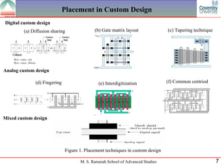
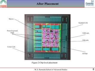
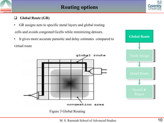
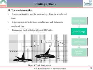
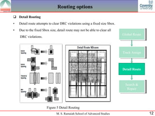
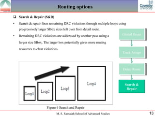
The document discusses placement and routing in full custom VLSI design. Placement involves techniques like diffusion sharing, gate matrix layout, and common centroid to optimize area and performance. Routing creates physical interconnects and involves global routing, track assignment, detail routing, and search and repair to meet timing constraints while resolving design rule checking violations. The quality of placement impacts routability, and routing aims to minimize delay along critical paths through techniques like buffer insertion and wire sizing.


