Downloaded 177 times

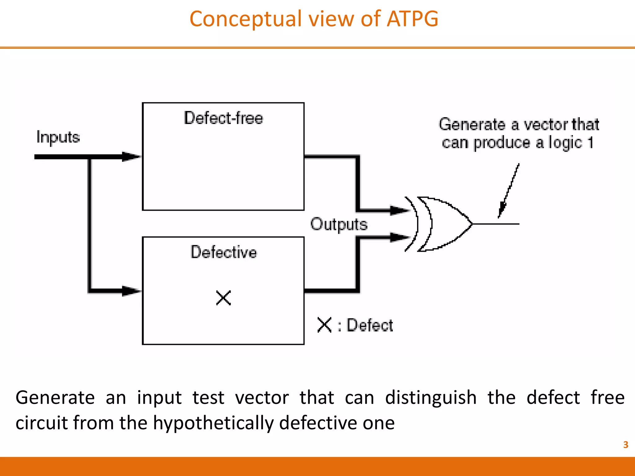
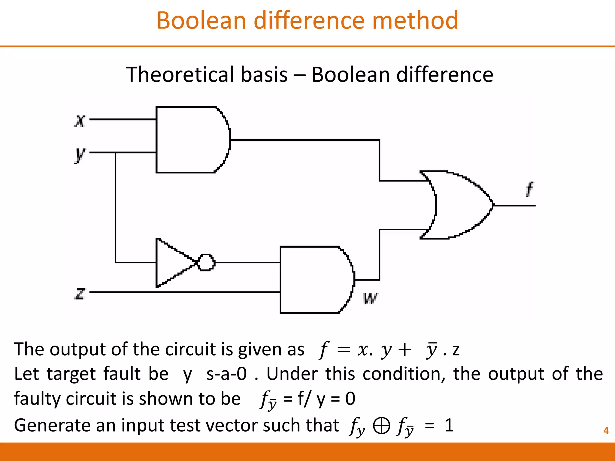
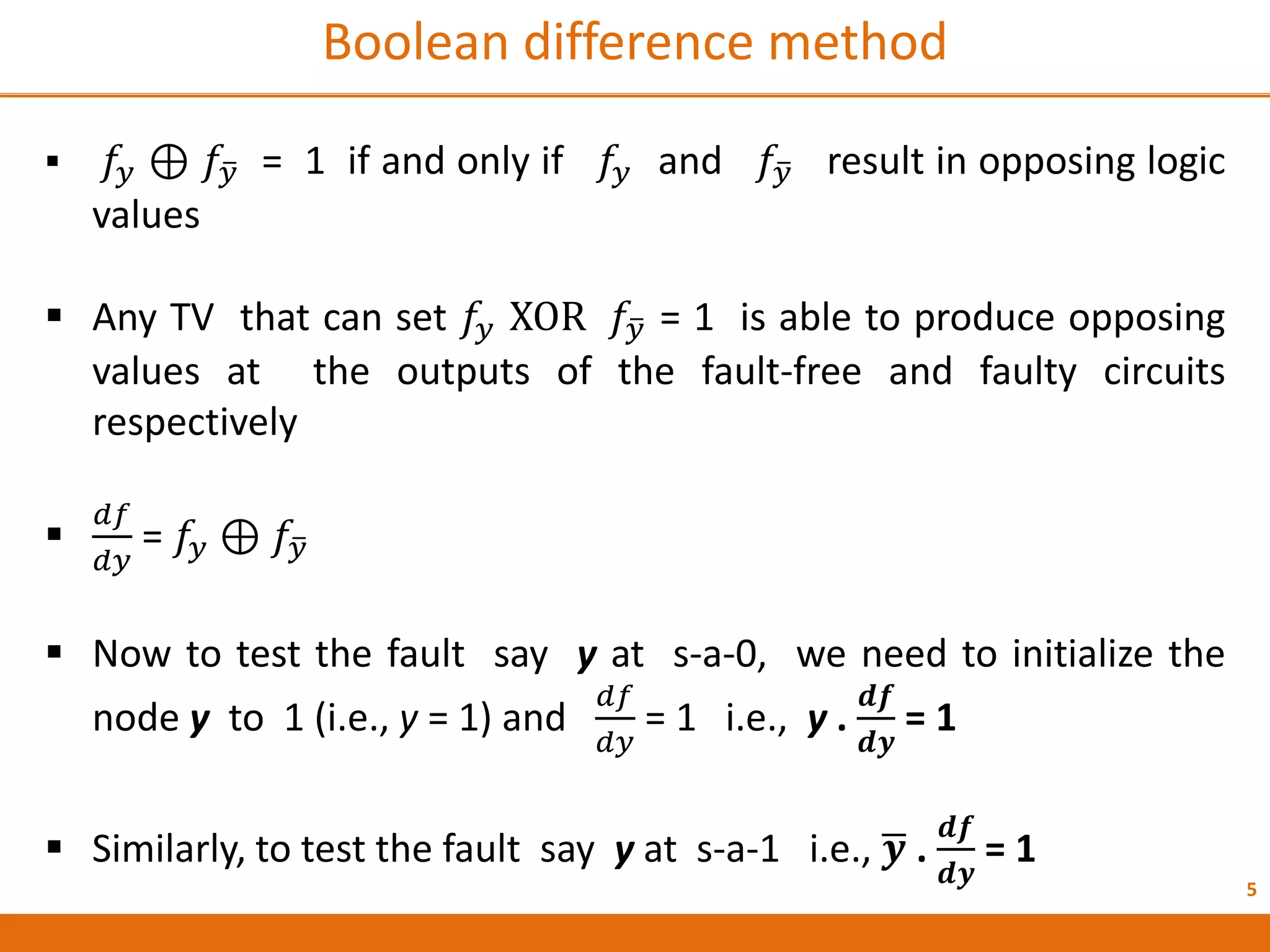
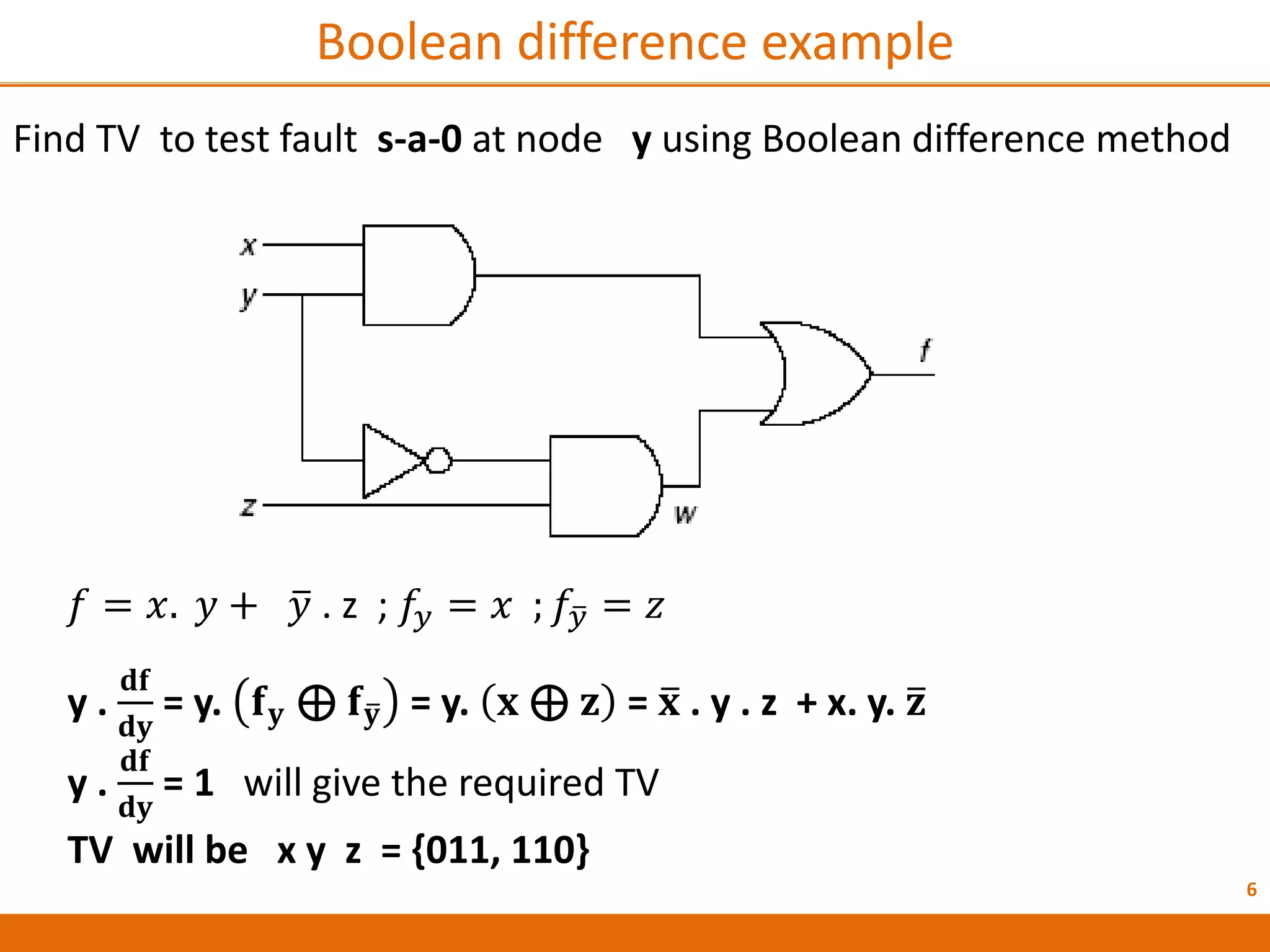
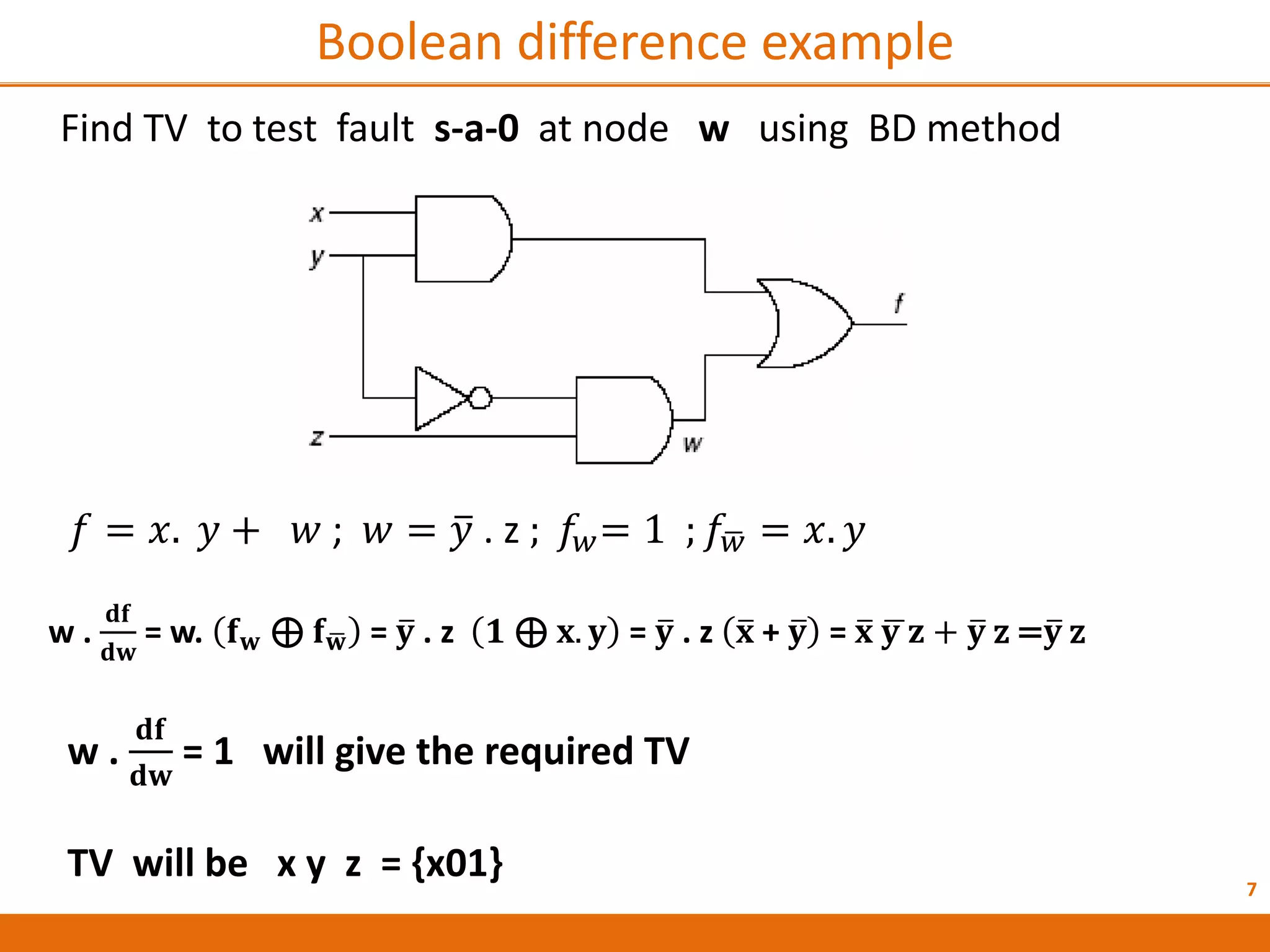
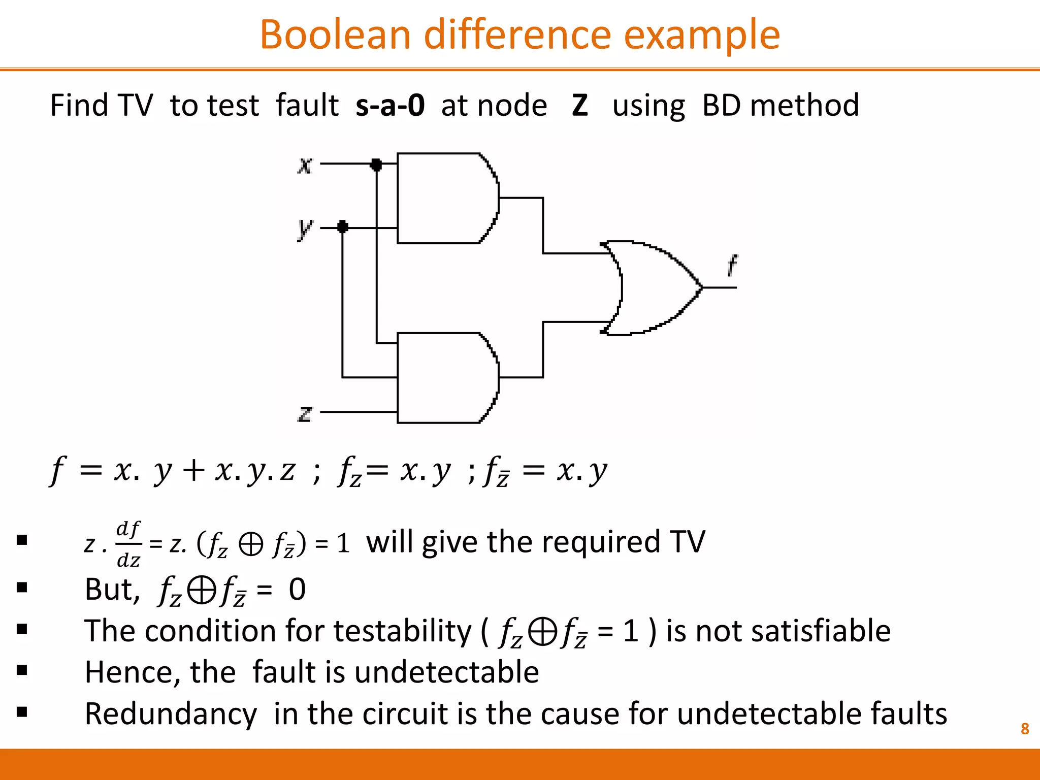


The Boolean difference method generates test vectors to distinguish between fault-free and faulty circuits. It works by calculating the Boolean difference between the outputs of the fault-free and faulty circuits (fy ⊕ fy). Any test vector that causes fy ⊕ fy to equal 1 can detect the fault. The method finds test vectors to set a specific node y to its faulty value (0 or 1) while making fy ⊕ fy = 1. An example shows generating test vectors {011, 110} to detect a stuck-at-0 fault at node y. Undetectable faults occur when fy ⊕ fy is always 0 due to circuit redundancy.