Download to read offline

![07/03/2019 Aravinda K., Dept. of E&C, NHCE, Bengaluru 28
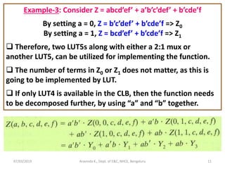
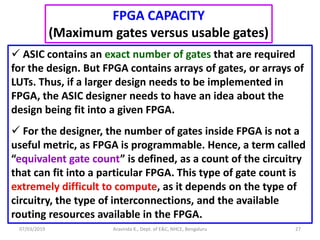
One method for computing the equivalent gate count for a
CLB is as follows: 2:1 mux = 4 gates, 3-input XOR gate = 6
gates, 4-input XOR gate = 9 gates, Flip-flop = 7 gates, and so
on. Thus, the equivalent gate count for a CLB can be obtained.
The total gate count can be estimated, by multiplying the
equivalent gate count with the number of CLBs in the FPGA.
In general, this type of gate count is likely to be higher than
the gate count of the practical circuitry that is being realized.
Another method is to use the Benchmark circuits (e.g.:
Benchmark suite prepared by PREP [Programmable
Electronics Performance company]). For example, if an ASIC
contains 2000 gates, and if an FPGA can fit 20 copies of the
ASIC, with no routing between the copies, then the maximum
gate count of the FPGA can be considered as 40,000.](https://image.slidesharecdn.com/sdhdlece43-m5-200302071342/85/System-design-using-HDL-Module-5-28-320.jpg)
![07/03/2019 Aravinda K., Dept. of E&C, NHCE, Bengaluru 31
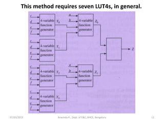
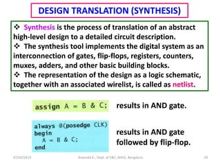
Synthesis of a
‘case’ statement
module case_eg (a,b);
input [1:0] a;
output reg [1:0] b;
always @(a)
begin
case (a)
0: b<=1;
1: b<=3;
2: b<=0;
3: b<=1;
endcase
end
endmodule
Synthesized circuit before optimization
Logic
optimization
Synthesized circuit after optimization](https://image.slidesharecdn.com/sdhdlece43-m5-200302071342/85/System-design-using-HDL-Module-5-31-320.jpg)
![07/03/2019 Aravinda K., Dept. of E&C, NHCE, Bengaluru 32
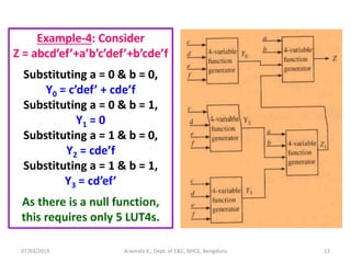
Unintentional
latch creation
Module latch_eg (a,b);
input [1:0] a;
output reg b;
always @(a)
begin
case (a)
0: b<=1;
1: b<=0;
2: b<=1;
endcase
end
endmodule
Initial output of naïve synthesizer
Optimized output of naïve synthesizer](https://image.slidesharecdn.com/sdhdlece43-m5-200302071342/85/System-design-using-HDL-Module-5-32-320.jpg)
![07/03/2019 Aravinda K., Dept. of E&C, NHCE, Bengaluru 33
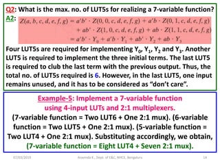
Output of
optimizing
synthesizer
Output of
naïve
synthesizer
Solution to
eliminate latch
Module latch_eg (a,b);
input [1:0] a;
output reg b;
always @(a)
begin
case (a)
0: b<=1;
1: b<=0;
2: b<=1;
3: b<=0;
endcase
end
endmodule](https://image.slidesharecdn.com/sdhdlece43-m5-200302071342/85/System-design-using-HDL-Module-5-33-320.jpg)
![07/03/2019 Aravinda K., Dept. of E&C, NHCE, Bengaluru 34
Synthesis of
‘if’ statements
if (A == 1’b1)
begin
nextstate <= 3;
Z <= 1;
end
if (A == 1’b1)
begin
nextstate <= 3;
Z <= 1;
end
else
begin
nextstate <= 2;
Z <= 0;
end
Ambiguous code,
that results in latch Unambiguous code
module if_eg (A,B,C,D,E,Z);
input A,B;
input [2:0] C,D,E;
output reg [2:0] Z;
always @(A or B)
begin
if (A == 1’b1)
Z <= C;
else if (B == 1’b0)
Z <= D;
else
Z <= E;
end
endmodule
Synthesized
output](https://image.slidesharecdn.com/sdhdlece43-m5-200302071342/85/System-design-using-HDL-Module-5-34-320.jpg)
![07/03/2019 Aravinda K., Dept. of E&C, NHCE, Bengaluru 35
Synthesis of arithmetic components
module ar_eg (clk,A,B,ge,acc,count);
input clk;
input [3:0] A,B;
inout [3:0] acc,count;
output ge;
reg [3:0] acc_t, count_t;
assign acc = acc_t;
assign count = count_t;
assign ge = (A >= B);
always @(posedge clk)
begin
acc_t <= acc +B;
count_t <= count + 1;
end
endmodule
Synthesized output](https://image.slidesharecdn.com/sdhdlece43-m5-200302071342/85/System-design-using-HDL-Module-5-35-320.jpg)
![07/03/2019 Aravinda K., Dept. of E&C, NHCE, Bengaluru 36
Example-7: What hardware gets
resulted for the statement,
assign LE = (A <= B);
where A and B are 4-bit vectors?
The symbol “<=” is a relational
operator over here.
The following statement
inside the ‘always’ block,
LE <= (A <= B);
results in the same hardware.
Example-8: What is the
optimized hardware for,
assign EQ3 = (A == 3);
where A is 4-bit vector?
A naïve synthesizer may
produce a 4-bit comparator,
with ‘A’ and ‘3’ as inputs.
For optimization, the
statement can be altered as:
assign EQ3 =
~A[3]&~A[2]&A[1]&A[0];](https://image.slidesharecdn.com/sdhdlece43-m5-200302071342/85/System-design-using-HDL-Module-5-36-320.jpg)
![07/03/2019 Aravinda K., Dept. of E&C, NHCE, Bengaluru 38
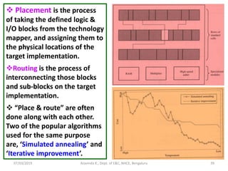
MAPPING, PLACEMENT AND ROUTING
These are the 3 major steps that happen, to transform
the design that is in the netlist form, to the appropriate
target technology (MPGA, CPLD, FPGA, ASIC).
Mapping is the process of translating the design into the
available building blocks in the target technology. [e.g.: LUT
with mux (Xilinx), Mux with gates (Microsemi)].
In other words, it is the process of binding the technology-
dependent circuits of the target technology to the technology-
independent circuits that are in the design.
In case of FPGA, the design has to be mapped into muxes,
LUTs etc. In case of ASIC, the design has to be mapped into the
standard cells that are available in the library (e.g.: logic gates,
muxes, decoders, encoders, comparators, counters etc.)](https://image.slidesharecdn.com/sdhdlece43-m5-200302071342/85/System-design-using-HDL-Module-5-38-320.jpg)


The document provides a detailed overview of FPGAs (Field Programmable Gate Arrays) and various design considerations, including the use of configurable logic blocks, LUTs (Look-Up Tables), and multiplexers for implementing digital functions. It discusses examples of designing specific components like multiplexers and shift registers, the costs of programmability, and methods for state machine implementation. Additionally, it outlines important FPGA architecture features and the associated trade-offs between programmability and hardware efficiency.