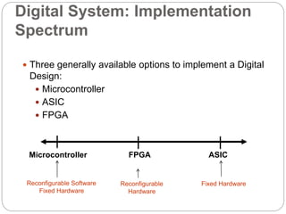
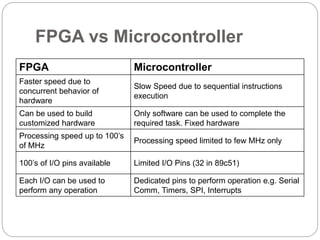
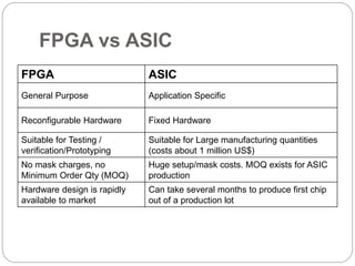
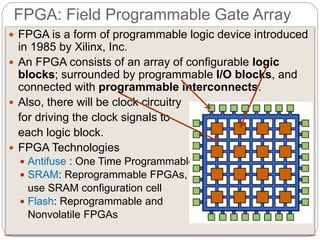
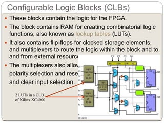
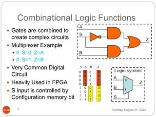
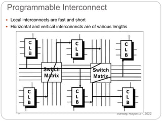
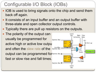
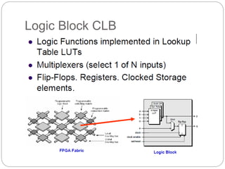
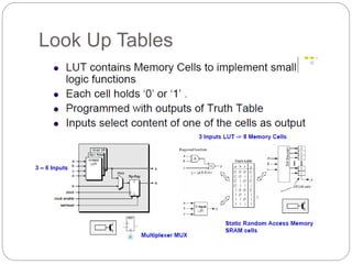
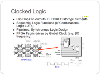
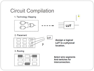
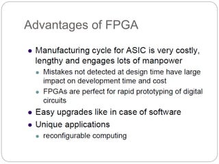
 Three generally available options to implement a Digital
Design:
 Microcontroller
 ASIC
 FPGA
Digital System: Implementation
Spectrum
Microcontroller FPGA ASIC
Reconfigurable Software
Fixed Hardware
Reconfigurable
Hardware
Fixed Hardware
FPGA vs Microcontroller
FPGA Microcontroller
Faster speed due to
concurrent behavior of
hardware
Slow Speed due to sequential instructions
execution
Can be used to build
customized hardware
Only software can be used to complete the
required task. Fixed hardware
Processing speed up to 100’s
of MHz
Processing speed limited to few MHz only
100’s of I/O pins available Limited I/O Pins (32 in 89c51)
Each I/O can be used to
perform any operation
Dedicated pins to perform operation e.g. Serial
Comm, Timers, SPI, Interrupts
FPGA vs ASIC
FPGA ASIC
General Purpose Application Specific
Reconfigurable Hardware Fixed Hardware
Suitable for Testing /
verification/Prototyping
Suitable for Large manufacturing quantities
(costs about 1 million US$)
No mask charges, no
Minimum Order Qty (MOQ)
Huge setup/mask costs. MOQ exists for ASIC
production
Hardware design is rapidly
available to market
Can take several months to produce first chip
out of a production lot
Digital Logic
FPGA: Field Programmable Gate Array
Sunday, August 21, 2022
www.iiu.edu.pk
5
 FPGA is a form of programmable logic device introduced
in 1985 by Xilinx, Inc.
 An FPGA consists of an array of configurable logic
blocks; surrounded by programmable I/O blocks, and
connected with programmable interconnects.
 Also, there will be clock circuitry
for driving the clock signals to
each logic block.
 FPGA Technologies
 Antifuse : One Time Programmable
 SRAM: Reprogrammable FPGAs,
use SRAM configuration cell
 Flash: Reprogrammable and
Nonvolatile FPGAs
Sunday, August 21, 2022
ww.iiu.edu.pk 6
 These blocks contain the logic for the FPGA.
 The block contains RAM for creating combinatorial logic
functions, also known as lookup tables (LUTs).
 It also contains flip-flops for clocked storage elements,
and multiplexers to route the logic within the block and to
and from external resources.
 The multiplexers also allow
polarity selection and reset
and clear input selection.
Configurable Logic Blocks (CLBs)
2 LUTs in a CLB
of Xilinx XC4000
 Gates are combined to
create complex circuits
 Multiplexer Example
 If S=0, Z=A
 If S=1, Z=B
 Very Common Digital
Circuit
 Heavily Used in FPGA
 S input is controlled by
Configuration memory bit
Combinational Logic Functions
Sunday, August 21, 2022
7
ww.iiu.edu.pk
0
0
1
1
1
0
1
Z
A
0
B
0
0
0
0
S
0
1
1
0
0
0
1
1
1
0
1
0
1
1
1
1
1
0
1
0
Programmable Interconnect
Sunday, August 21, 2022
8
 Local interconnects are fast and short
 Horizontal and vertical interconnects are of various lengths
Sunday, August 21, 2022
ww.iiu.edu.pk 9
 IOB is used to bring signals onto the chip and send them
back off again.
 It consists of an input buffer and an output buffer with
three-state and open collector output controls.
 Typically there are pull up resistors on the outputs.
 The polarity of the output can
usually be programmed for
active high or active low output,
and often the slew rate of the
output can be programmed for
fast or slow rise and fall times.
Configurable I/O Block (IOBs)
Logic Block CLB
Look Up Tables
Clocked Logic
Circuit Compilation
Advantages of FPGA
Major FPGA Vendors

Lecture Slide (1).pptx

  • 1.
     Three generallyavailable options to implement a Digital Design:  Microcontroller  ASIC  FPGA Digital System: Implementation Spectrum Microcontroller FPGA ASIC Reconfigurable Software Fixed Hardware Reconfigurable Hardware Fixed Hardware
  • 2.
    FPGA vs Microcontroller FPGAMicrocontroller Faster speed due to concurrent behavior of hardware Slow Speed due to sequential instructions execution Can be used to build customized hardware Only software can be used to complete the required task. Fixed hardware Processing speed up to 100’s of MHz Processing speed limited to few MHz only 100’s of I/O pins available Limited I/O Pins (32 in 89c51) Each I/O can be used to perform any operation Dedicated pins to perform operation e.g. Serial Comm, Timers, SPI, Interrupts
  • 3.
    FPGA vs ASIC FPGAASIC General Purpose Application Specific Reconfigurable Hardware Fixed Hardware Suitable for Testing / verification/Prototyping Suitable for Large manufacturing quantities (costs about 1 million US$) No mask charges, no Minimum Order Qty (MOQ) Huge setup/mask costs. MOQ exists for ASIC production Hardware design is rapidly available to market Can take several months to produce first chip out of a production lot
  • 4.
  • 5.
    FPGA: Field ProgrammableGate Array Sunday, August 21, 2022 www.iiu.edu.pk 5  FPGA is a form of programmable logic device introduced in 1985 by Xilinx, Inc.  An FPGA consists of an array of configurable logic blocks; surrounded by programmable I/O blocks, and connected with programmable interconnects.  Also, there will be clock circuitry for driving the clock signals to each logic block.  FPGA Technologies  Antifuse : One Time Programmable  SRAM: Reprogrammable FPGAs, use SRAM configuration cell  Flash: Reprogrammable and Nonvolatile FPGAs
  • 6.
    Sunday, August 21,2022 ww.iiu.edu.pk 6  These blocks contain the logic for the FPGA.  The block contains RAM for creating combinatorial logic functions, also known as lookup tables (LUTs).  It also contains flip-flops for clocked storage elements, and multiplexers to route the logic within the block and to and from external resources.  The multiplexers also allow polarity selection and reset and clear input selection. Configurable Logic Blocks (CLBs) 2 LUTs in a CLB of Xilinx XC4000
  • 7.
     Gates arecombined to create complex circuits  Multiplexer Example  If S=0, Z=A  If S=1, Z=B  Very Common Digital Circuit  Heavily Used in FPGA  S input is controlled by Configuration memory bit Combinational Logic Functions Sunday, August 21, 2022 7 ww.iiu.edu.pk 0 0 1 1 1 0 1 Z A 0 B 0 0 0 0 S 0 1 1 0 0 0 1 1 1 0 1 0 1 1 1 1 1 0 1 0
  • 8.
    Programmable Interconnect Sunday, August21, 2022 8  Local interconnects are fast and short  Horizontal and vertical interconnects are of various lengths
  • 9.
    Sunday, August 21,2022 ww.iiu.edu.pk 9  IOB is used to bring signals onto the chip and send them back off again.  It consists of an input buffer and an output buffer with three-state and open collector output controls.  Typically there are pull up resistors on the outputs.  The polarity of the output can usually be programmed for active high or active low output, and often the slew rate of the output can be programmed for fast or slow rise and fall times. Configurable I/O Block (IOBs)
  • 10.
  • 11.
  • 12.
  • 13.
  • 14.
  • 15.