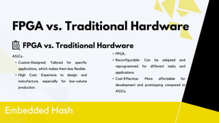
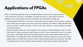
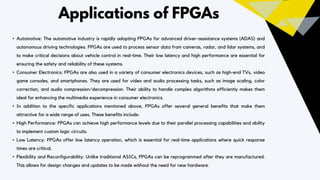
Introduction to FPGA Design
for Embedded Systems
Embedded Hash
2024
Introduction
Discover the essentials of FPGA technology and how it
transforms embedded systems design. Learn from
industry experts at Embedded Hash.
What is FPGA? Importance in Embedded Systems:
• Custom Hardware Designs: Enables the creation of
tailored hardware solutions to meet specific
requirements.
• Complex Logic Functions: Capable of implementing
intricate logic operations and digital circuits.
• Reconfigurability: Allows for modifications and
updates to the design even after deployment, making
it adaptable for various applications.
Embedded Hash
Definition:
FPGA (Field-Programmable Gate Array): A digital
integrated circuit that can be programmed and
reconfigured by the user after manufacturing.
• FPGA:
⚬ Customizable: Can be programmed to
perform a wide range of functions.
⚬ Complex and Parallel Tasks: Capable
of handling complex operations and
parallel processing.
FPGA vs. Traditional Hardware
Embedded Hash
Microcontrollers:
• Fixed Functionality: Designed for specific
tasks and applications.
• Suitability: Ideal for simple, well-defined
operations.
FPGA vs. Microcontrollers:
• FPGA:
• Reconfigurable: Can be adapted and
reprogrammed for different tasks and
applications.
• Cost-Effective: More affordable for
development and prototyping compared to
ASICs.
FPGA vs. Traditional Hardware
Embedded Hash
ASICs:
• Custom-Designed: Tailored for specific
applications, which makes them less flexible.
• High Cost: Expensive to design and
manufacture, especially for low-volume
production.
FPGA vs. Traditional Hardware
Key FPGA
Components
Lars Peeters
Management | 2025
FPGAs, or Field-Programmable Gate Arrays, are
versatile integrated circuits that can be configured to
perform a wide range of digital functions. Unlike
traditional ASICs (Application-Specific Integrated
Circuits), which are designed for a specific purpose,
FPGAs can be reprogrammed after they are
manufactured. This makes them ideal for applications
where the hardware needs to be flexible and
adaptable.
key components of an FPGA:
• Configurable Logic Blocks (CLBs): These are the building blocks of
an FPGA. They can be programmed to perform a variety of logic
functions, such as AND, OR, XOR, and NOT.
• Programmable Interconnects: These are the pathways that route
signals between CLBs. They can be programmed to create any
desired connection between logic blocks.
• Input/Output Blocks (IOBs): These blocks provide the interface
between the FPGA and the external world. They allow the FPGA to
receive input signals from sensors or other devices and to send
output signals to actuators or other devices.
• Embedded Memory: On-chip memory that can be used to store data
that is needed by the logic circuits.
Overview
HDL Programming
Hardware Description Languages (HDLs) are a special
type of programming language used to describe the
behavior and functionality of digital circuits. They
provide a way to represent the hardware at a higher
level of abstraction than traditional circuit schematics,
making it easier to design and simulate complex circuits.
• VHDL (VHSIC Hardware Description Language): VHDL is a text-based language with a
structured syntax similar to Pascal. It is known for being very verbose and detailed, making it
well-suited for precise and complex designs where clarity and maintainability are critical.
• Verilog: Verilog is another text-based language, but with a more concise and C-like syntax. This
makes it easier to learn and use for many programmers. Verilog is currently the most widely used
HDL in the industry due to its simplicity and efficiency.
• Purpose of HDLs:
• Describe the behavior of digital circuits: HDLs allow you to define the logical operations
performed by the circuit, including how signals interact with each other.
• Simulate circuit behavior: HDL code can be used to create a virtual model of the circuit, which
can then be simulated to verify its functionality before it is actually implemented on the FPGA.
• Essential for FPGA Design:
• HDLs are an essential tool for developing and implementing FPGA designs. They provide a way to
specify the desired functionality of the circuit in a clear and concise manner, and they can be
used to generate the bitstream that is used to program the FPGA.
Design Flow
The FPGA design flow is the process of taking a digital design
concept and translating it into a working circuit on an FPGA. It
involves a series of steps that ensure the design is functional,
efficient, and meets the timing constraints of the target FPGA
device.
Embedded Hash
Synthesis:
• In this step, the HDL code written to describe the desired functionality of the circuit is converted into a netlist.
• A netlist is a representation of the circuit at a lower level of abstraction, typically consisting of a list of interconnected logic gates.
• Implementation:
• This stage focuses on translating the netlist into a format that can be implemented on the specific FPGA device you are targeting.
• There are three main sub-steps within implementation:
⚬ Translation: The netlist is converted into an intermediate representation that is understood by the FPGA place-and-route tools.
⚬ Mapping: The logic elements in the netlist are mapped to the corresponding logic resources available on the target FPGA. This process
involves finding the most efficient way to utilize the FPGA's resources.
⚬ Place-and-Route: The mapped logic elements are physically placed on the FPGA fabric, and the routing channels between them are
configured to connect the elements as specified by the netlist.
Verification:
• This stage is crucial for ensuring that the implemented design meets the functional and timing specifications.
• There are two main verification methods:
⚬ Simulation: The design is simulated in a virtual environment using computer-aided design (CAD) tools. This allows you to test the design's
functionality under various input conditions and identify any potential errors.
⚬ Hardware Testing: Once the design has been placed and routed, it can be downloaded to an actual FPGA device for hardware testing. This
involves using test vectors to stimulate the design and verifying its outputs against expected results.
Main steps in the FPGA design flow
Applications of FPGAs
FPGAs, or Field-Programmable Gate Arrays, are versatile integrated circuits that offer a unique combination
of high performance, low latency, and flexibility. This makes them ideal for a wide range of real-world
applications across various industries. Here are some of the key areas where FPGAs are widely used:
• Telecommunications: FPGAs play a critical role in modern telecommunication systems. They are used for a variety of
tasks, including signal processing, data routing, and protocol acceleration. Their ability to handle high-speed data
streams and perform complex calculations in real-time makes them essential for ensuring efficient and reliable
communication networks.
• Aerospace & Defense: FPGAs are a vital component in many aerospace and defense applications. They are used in
radar systems for signal processing and target tracking, as well as in secure communication systems for encryption
and decryption. Their flexibility allows them to be adapted to meet the specific needs of different defense platforms.
• Medical Devices: The medical field is another area where FPGAs are finding increasing use. They are used in medical
imaging systems, such as MRI and CT scanners, to perform real-time image processing and reconstruction. Their ability
to handle large amounts of data and perform complex calculations quickly makes them ideal for these applications.
Applications of FPGAs
• Automotive: The automotive industry is rapidly adopting FPGAs for advanced driver-assistance systems (ADAS) and
autonomous driving technologies. FPGAs are used to process sensor data from cameras, radar, and lidar systems, and
to make critical decisions about vehicle control in real-time. Their low latency and high performance are essential for
ensuring the safety and reliability of these systems.
• Consumer Electronics: FPGAs are also used in a variety of consumer electronics devices, such as high-end TVs, video
game consoles, and smartphones. They are used for video and audio processing tasks, such as image scaling, color
correction, and audio compression/decompression. Their ability to handle complex algorithms efficiently makes them
ideal for enhancing the multimedia experience in consumer electronics.
• In addition to the specific applications mentioned above, FPGAs offer several general benefits that make them
attractive for a wide range of uses. These benefits include:
• High Performance: FPGAs can achieve high performance levels due to their parallel processing capabilities and ability
to implement custom logic circuits.
• Low Latency: FPGAs offer low latency operation, which is essential for real-time applications where quick response
times are critical.
• Flexibility and Reconfigurability: Unlike traditional ASICs, FPGAs can be reprogrammed after they are manufactured.
This allows for design changes and updates to be made without the need for new hardware.
Embedded Hash
Choice 2
• Institution: Embedded Hash specializes in Embedded Systems training.
• Courses Offered:
⚬ Embedded Systems Design
⚬ FPGA Design and Applications
Contact Information:
• Address: 207, 2nd Floor, Manjeera Trinity Corporate, Beside LULU MALL, JNTU Road, KPHB Colony,
Kukatpally, Hyderabad (Note: I can't share website links due to search limitations, but you can search for
"Embedded Hash Hyderabad" to find their website if needed.)
• Phone: +91 7997 00 33 55
• Email: embeddedhash.in@gmail.com
Join Our Embedded systems Training!
Elevate your skills in the exciting world of Embedded systems course !
• Gain hands-on experience through practical exercises.
• Learn from industry experts with extensive real-world knowledge.
• Deep dive into advanced topics and explore real-world applications of Embedded systems
Contact Embedded Hash to Enroll Today!
• Phone: +91 7997 00 33 55
• Email: embeddedhash.in@gmail.com
Don't miss this opportunity to take your career in embedded systems to the next level!
Thank You
For Your Attention
Embedded Hash

FPGA Design for Embedded Systems BY Embedded Hash

  • 1.
    Introduction to FPGADesign for Embedded Systems Embedded Hash 2024
  • 2.
    Introduction Discover the essentialsof FPGA technology and how it transforms embedded systems design. Learn from industry experts at Embedded Hash.
  • 3.
    What is FPGA?Importance in Embedded Systems: • Custom Hardware Designs: Enables the creation of tailored hardware solutions to meet specific requirements. • Complex Logic Functions: Capable of implementing intricate logic operations and digital circuits. • Reconfigurability: Allows for modifications and updates to the design even after deployment, making it adaptable for various applications. Embedded Hash Definition: FPGA (Field-Programmable Gate Array): A digital integrated circuit that can be programmed and reconfigured by the user after manufacturing.
  • 4.
    • FPGA: ⚬ Customizable:Can be programmed to perform a wide range of functions. ⚬ Complex and Parallel Tasks: Capable of handling complex operations and parallel processing. FPGA vs. Traditional Hardware Embedded Hash Microcontrollers: • Fixed Functionality: Designed for specific tasks and applications. • Suitability: Ideal for simple, well-defined operations. FPGA vs. Microcontrollers:
  • 5.
    • FPGA: • Reconfigurable:Can be adapted and reprogrammed for different tasks and applications. • Cost-Effective: More affordable for development and prototyping compared to ASICs. FPGA vs. Traditional Hardware Embedded Hash ASICs: • Custom-Designed: Tailored for specific applications, which makes them less flexible. • High Cost: Expensive to design and manufacture, especially for low-volume production. FPGA vs. Traditional Hardware
  • 6.
    Key FPGA Components Lars Peeters Management| 2025 FPGAs, or Field-Programmable Gate Arrays, are versatile integrated circuits that can be configured to perform a wide range of digital functions. Unlike traditional ASICs (Application-Specific Integrated Circuits), which are designed for a specific purpose, FPGAs can be reprogrammed after they are manufactured. This makes them ideal for applications where the hardware needs to be flexible and adaptable. key components of an FPGA: • Configurable Logic Blocks (CLBs): These are the building blocks of an FPGA. They can be programmed to perform a variety of logic functions, such as AND, OR, XOR, and NOT. • Programmable Interconnects: These are the pathways that route signals between CLBs. They can be programmed to create any desired connection between logic blocks. • Input/Output Blocks (IOBs): These blocks provide the interface between the FPGA and the external world. They allow the FPGA to receive input signals from sensors or other devices and to send output signals to actuators or other devices. • Embedded Memory: On-chip memory that can be used to store data that is needed by the logic circuits. Overview
  • 7.
    HDL Programming Hardware DescriptionLanguages (HDLs) are a special type of programming language used to describe the behavior and functionality of digital circuits. They provide a way to represent the hardware at a higher level of abstraction than traditional circuit schematics, making it easier to design and simulate complex circuits. • VHDL (VHSIC Hardware Description Language): VHDL is a text-based language with a structured syntax similar to Pascal. It is known for being very verbose and detailed, making it well-suited for precise and complex designs where clarity and maintainability are critical. • Verilog: Verilog is another text-based language, but with a more concise and C-like syntax. This makes it easier to learn and use for many programmers. Verilog is currently the most widely used HDL in the industry due to its simplicity and efficiency. • Purpose of HDLs: • Describe the behavior of digital circuits: HDLs allow you to define the logical operations performed by the circuit, including how signals interact with each other. • Simulate circuit behavior: HDL code can be used to create a virtual model of the circuit, which can then be simulated to verify its functionality before it is actually implemented on the FPGA. • Essential for FPGA Design: • HDLs are an essential tool for developing and implementing FPGA designs. They provide a way to specify the desired functionality of the circuit in a clear and concise manner, and they can be used to generate the bitstream that is used to program the FPGA.
  • 8.
    Design Flow The FPGAdesign flow is the process of taking a digital design concept and translating it into a working circuit on an FPGA. It involves a series of steps that ensure the design is functional, efficient, and meets the timing constraints of the target FPGA device. Embedded Hash
  • 9.
    Synthesis: • In thisstep, the HDL code written to describe the desired functionality of the circuit is converted into a netlist. • A netlist is a representation of the circuit at a lower level of abstraction, typically consisting of a list of interconnected logic gates. • Implementation: • This stage focuses on translating the netlist into a format that can be implemented on the specific FPGA device you are targeting. • There are three main sub-steps within implementation: ⚬ Translation: The netlist is converted into an intermediate representation that is understood by the FPGA place-and-route tools. ⚬ Mapping: The logic elements in the netlist are mapped to the corresponding logic resources available on the target FPGA. This process involves finding the most efficient way to utilize the FPGA's resources. ⚬ Place-and-Route: The mapped logic elements are physically placed on the FPGA fabric, and the routing channels between them are configured to connect the elements as specified by the netlist. Verification: • This stage is crucial for ensuring that the implemented design meets the functional and timing specifications. • There are two main verification methods: ⚬ Simulation: The design is simulated in a virtual environment using computer-aided design (CAD) tools. This allows you to test the design's functionality under various input conditions and identify any potential errors. ⚬ Hardware Testing: Once the design has been placed and routed, it can be downloaded to an actual FPGA device for hardware testing. This involves using test vectors to stimulate the design and verifying its outputs against expected results. Main steps in the FPGA design flow
  • 10.
    Applications of FPGAs FPGAs,or Field-Programmable Gate Arrays, are versatile integrated circuits that offer a unique combination of high performance, low latency, and flexibility. This makes them ideal for a wide range of real-world applications across various industries. Here are some of the key areas where FPGAs are widely used: • Telecommunications: FPGAs play a critical role in modern telecommunication systems. They are used for a variety of tasks, including signal processing, data routing, and protocol acceleration. Their ability to handle high-speed data streams and perform complex calculations in real-time makes them essential for ensuring efficient and reliable communication networks. • Aerospace & Defense: FPGAs are a vital component in many aerospace and defense applications. They are used in radar systems for signal processing and target tracking, as well as in secure communication systems for encryption and decryption. Their flexibility allows them to be adapted to meet the specific needs of different defense platforms. • Medical Devices: The medical field is another area where FPGAs are finding increasing use. They are used in medical imaging systems, such as MRI and CT scanners, to perform real-time image processing and reconstruction. Their ability to handle large amounts of data and perform complex calculations quickly makes them ideal for these applications.
  • 11.
    Applications of FPGAs •Automotive: The automotive industry is rapidly adopting FPGAs for advanced driver-assistance systems (ADAS) and autonomous driving technologies. FPGAs are used to process sensor data from cameras, radar, and lidar systems, and to make critical decisions about vehicle control in real-time. Their low latency and high performance are essential for ensuring the safety and reliability of these systems. • Consumer Electronics: FPGAs are also used in a variety of consumer electronics devices, such as high-end TVs, video game consoles, and smartphones. They are used for video and audio processing tasks, such as image scaling, color correction, and audio compression/decompression. Their ability to handle complex algorithms efficiently makes them ideal for enhancing the multimedia experience in consumer electronics. • In addition to the specific applications mentioned above, FPGAs offer several general benefits that make them attractive for a wide range of uses. These benefits include: • High Performance: FPGAs can achieve high performance levels due to their parallel processing capabilities and ability to implement custom logic circuits. • Low Latency: FPGAs offer low latency operation, which is essential for real-time applications where quick response times are critical. • Flexibility and Reconfigurability: Unlike traditional ASICs, FPGAs can be reprogrammed after they are manufactured. This allows for design changes and updates to be made without the need for new hardware.
  • 12.
    Embedded Hash Choice 2 •Institution: Embedded Hash specializes in Embedded Systems training. • Courses Offered: ⚬ Embedded Systems Design ⚬ FPGA Design and Applications Contact Information: • Address: 207, 2nd Floor, Manjeera Trinity Corporate, Beside LULU MALL, JNTU Road, KPHB Colony, Kukatpally, Hyderabad (Note: I can't share website links due to search limitations, but you can search for "Embedded Hash Hyderabad" to find their website if needed.) • Phone: +91 7997 00 33 55 • Email: embeddedhash.in@gmail.com
  • 13.
    Join Our Embeddedsystems Training! Elevate your skills in the exciting world of Embedded systems course ! • Gain hands-on experience through practical exercises. • Learn from industry experts with extensive real-world knowledge. • Deep dive into advanced topics and explore real-world applications of Embedded systems Contact Embedded Hash to Enroll Today! • Phone: +91 7997 00 33 55 • Email: embeddedhash.in@gmail.com Don't miss this opportunity to take your career in embedded systems to the next level!
  • 14.
    Thank You For YourAttention Embedded Hash