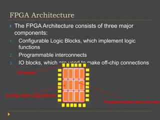
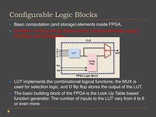
SlideShare a Scribd company logo
FPGA: Architecture and
Applications
Sudhanshu Janwadkar
SV National Institute of Technology, Surat
May 3rd, 2020
What are FPGAs?
 FPGA : Field Programmable Gate Array.
 It is a type of programmable chip.
 FPGAs contain programmable logic blocks and
interconnection circuits.
 These can be programmed or reprogrammed to the
required functionality after manufacturing.
What are FPGAs?
 Field-programmable gate arrays (FPGAs) act as the
boundary between hardware and software.
 Microcontrollers program the chip with a series of
instructions. However, FPGA creates logic
structures built from gates inside the chip, in
accordance with the logic to be implemented.
 Therefore, they are customizable circuits
- i.e. They can be updated by designers after
manufacturing or deployment in the field.
FPGA Boards
 FPGAs are available as part of circuit boards which
contain multiple optional other peripherals such as
switches, LEDs, 7-segment displays, ADCs and
DACs, VGA, etc.
 Examples:
Name: Nexys- A7 Mimas A7 Zynq-700
Manufacturer: Digilent Inc. Numato Lab Digilent
Inc.
FPGAs
FPGAs versus ASICs
 The major advantage of FPGAs over ASIC is its
programmability feature and low time to market.
 ASICs takes months to manufacture and are
not flexible in terms of functionality.
 The total design cost of ASIC is higher than FPGA,
however, FPGA have a higher per unit cost than
ASICs.
 Once designed and verified, ASICs can be
produced in huge quantities at very low costs,
almost 100 times cheaper than FPGAs.
 FPGAs consume more area and are many folds
power hungry than ASICs.
 Despite all, FPGA serve as most popular platform for
Rapid prototyping of FPGAs.
FPGA Architecture
 The FPGA Architecture consists of three major
components:
1. Configurable Logic Blocks, which implement logic
functions
2. Programmable interconnects
3. IO blocks, which are used to make off-chip connections
IO blocks
Configurable Logic Blocks
Programmable Interconnects
Configurable Logic Blocks
 Basic computation (and storage) elements inside FPGA.
 Contains LUTs (Look-up Tables) which compute the logic output,
Flip-flops and Multiplexers.
 LUT implements the combinational logical functions; the MUX is
used for selection logic, and D flip flop stores the output of the LUT.
 The basic building block of the FPGA is the Look Up Table based
function generator. The number of inputs to the LUT vary from 4 to 6
or even more.
 Modern FPGAs contain a heterogeneous mixture of
different blocks like dedicated memory blocks,
multiplexers.
 Configuration memory is used throughout the logic blocks
to control the specific function of each element.
 Present FPGA consists of about hundreds or thousands
of configurable logic blocks.
 For configuring the FPGA, software such as Xilinx ISE
are used. These software generate a bitstream file, which
then configures the logic blocks (LUTs) and the
interconnects.
Programmable Interconnects
 Interconnects establish the connection between
configurable logic blocks and Input / Output blocks to
complete a user-defined design unit.
 It consists of multiplexers, pass transistors and tri-
state buffers.
 Pass transistors and multiplexers are used in a logic
cluster to connect the logic elements.
IO Blocks
 Used to interface the logic blocks and routing
architecture to the external components.
 The I/O pad and the surrounding logic circuit form as
an I/O cell.
 These cells consume a large portion of the FPGA’s
area.
 With advancement, the basic FPGA Architecture has
developed through the addition of more specialized
programmable function blocks.
 The special functional blocks like ALUs, block RAM,
multiplexers, DSP-48, and microprocessors have been
added to the FPGA, due to the frequency of the need for
such resources for applications.
FPGA Design Flow
FPGA design comprises of :
1. design entry
2. design synthesis
3. design implementation
4. device programming and
5. design verification.
Design verification includes:
1. functional verification and
2. timing verification
Design Entry
 The design entry is done in different techniques like:
1. schematic based
2. hardware description language (HDL)
3. combination of both etc.
 If the designer wants to deal with hardware, then the
schematic entry is a good choice.
 If the designer thinks the design in an algorithmic
way, then the HDL is the better choice.
Design Synthesis
 This process translates VHDL code into a device
netlist format, i.e., a complete circuit with logical
elements.
 The design synthesis process will check the code
syntax and analyze the hierarchy of the design
architecture.
 This ensures the design optimized for the design
architecture.
 The netlist is saved as Native Generic Circuit (NGC)
file.
Design Implementation
 The implementation process consists of
1. Translate
 This process combines all the input netlists to the logic design
file which is saved as NGD (Native Generic Database) file.
Here the ports are assigned to the physical elements like pins,
switches in the design. This is stored in a file called User
Constraints File (UCF).
2. Map
 Mapping divides the circuit into sub-blocks such that they can
be fit into the FPGA logic blocks. Thus this process fits the
logic defined by NGD into the combinational Logic Blocks,
Input-Output Blocks and then generates an NCD file, which
represents the design mapped to the components of FPGA.
3. Routing
 The routing process places the sub-blocks from the mapping
process into the logic block according to the constraints and
then connects the logic blocks.
Device Programming
 The routed design must be loaded into the FPGA.
 This design must be converted into a format
supported by the FPGA.
 The routed NCD file is given to the BITGEN
program, which generates the BIT file.
 This BIT file is configured to the FPGA.
Design Verification
Design Verification is done at various stages.
1. Functional Simulation
 Functional simulation is performed post-translation
simulation. It gives the information about the logical
operation of the circuit.
2. Static Timing Simulation
 This is done post mapping. Post map timing report
gives the signal path delays. After place and route,
timing report takes the timing delay information. This
provides a complete timing summary of the design.
FPGA Applications
 Application domains:
FPGA Applications
 Emulation of entire large hardware systems via the
use of many interconnected FPGAs.
 ASIC prototyping or SoC prototyping
- method to prototype SoC and ASICs on FPGAs
for hardware verification and early software
development.
 Parallel Computing to meet requirements in machine
learning, computer vision, video surveillance etc.
 FPGAs provide a unique combination of highly
parallel custom computation and low-cost
computation.

More Related Content

Similar to FPGA Architecture and application

L12_PROGRAMMABLE+LOGIC+DEVICES+(PLD).ppt
L12_PROGRAMMABLE+LOGIC+DEVICES+(PLD).pptL12_PROGRAMMABLE+LOGIC+DEVICES+(PLD).ppt
L12_PROGRAMMABLE+LOGIC+DEVICES+(PLD).ppt
MikeTango5
 
Fpga
FpgaFpga
Project report of 2016 Trainee_final
Project report of 2016 Trainee_finalProject report of 2016 Trainee_final
Project report of 2016 Trainee_final
Akash Chowdhury
 
vlsi internal ppt on field programable gate array
vlsi internal ppt on field programable gate arrayvlsi internal ppt on field programable gate array
vlsi internal ppt on field programable gate array
SandeepPanigrahi13
 
module 1-2 - Design Methods, parameters and examples.pptx
module 1-2 - Design Methods, parameters and examples.pptxmodule 1-2 - Design Methods, parameters and examples.pptx
module 1-2 - Design Methods, parameters and examples.pptx
Maaz609108
 
FPGA Design, Architecture and Applications
FPGA Design, Architecture and ApplicationsFPGA Design, Architecture and Applications
FPGA Design, Architecture and Applications
Logic Fruit Technologies
 
Introduction to FPGAs
Introduction to FPGAsIntroduction to FPGAs
Introduction to FPGAs
Sudhanshu Janwadkar
 
91 94
91 9491 94
91 94
91 9491 94
A Review of FPGA-based design methodologies for efficient hardware Area estim...
A Review of FPGA-based design methodologies for efficient hardware Area estim...A Review of FPGA-based design methodologies for efficient hardware Area estim...
A Review of FPGA-based design methodologies for efficient hardware Area estim...
IOSR Journals
 
FPGA Intro
FPGA IntroFPGA Intro
FPGA Intro
naito88
 
FIELD PROGRAMMABLE GATE ARRAYS AND THEIR APPLICATIONS
FIELD PROGRAMMABLE GATE ARRAYS AND THEIR APPLICATIONSFIELD PROGRAMMABLE GATE ARRAYS AND THEIR APPLICATIONS
FIELD PROGRAMMABLE GATE ARRAYS AND THEIR APPLICATIONS
Professor at RYM Engineering College, Ballari
 
Lecture Slide (1).pptx
Lecture Slide (1).pptxLecture Slide (1).pptx
Lecture Slide (1).pptx
BilalMumtaz9
 
ASIC VS FPGA.ppt
ASIC VS FPGA.pptASIC VS FPGA.ppt
ASIC VS FPGA.ppt
gopakumar885691
 
4_BIT_ALU
4_BIT_ALU4_BIT_ALU
4_BIT_ALU
Sohel Siddique
 
Nt1310 Unit 5 Algorithm
Nt1310 Unit 5 AlgorithmNt1310 Unit 5 Algorithm
Nt1310 Unit 5 Algorithm
Angie Lee
 
International Journal of Computational Engineering Research(IJCER)
International Journal of Computational Engineering Research(IJCER) International Journal of Computational Engineering Research(IJCER)
International Journal of Computational Engineering Research(IJCER)
ijceronline
 
International Journal of Computational Engineering Research(IJCER)
International Journal of Computational Engineering Research(IJCER)International Journal of Computational Engineering Research(IJCER)
International Journal of Computational Engineering Research(IJCER)
ijceronline
 
FPGAPpr_final
FPGAPpr_finalFPGAPpr_final
FPGAPpr_final
Priyesh vJ
 
Fpga
FpgaFpga

Similar to FPGA Architecture and application (20)

L12_PROGRAMMABLE+LOGIC+DEVICES+(PLD).ppt
L12_PROGRAMMABLE+LOGIC+DEVICES+(PLD).pptL12_PROGRAMMABLE+LOGIC+DEVICES+(PLD).ppt
L12_PROGRAMMABLE+LOGIC+DEVICES+(PLD).ppt
 
Fpga
FpgaFpga
Fpga
 
Project report of 2016 Trainee_final
Project report of 2016 Trainee_finalProject report of 2016 Trainee_final
Project report of 2016 Trainee_final
 
vlsi internal ppt on field programable gate array
vlsi internal ppt on field programable gate arrayvlsi internal ppt on field programable gate array
vlsi internal ppt on field programable gate array
 
module 1-2 - Design Methods, parameters and examples.pptx
module 1-2 - Design Methods, parameters and examples.pptxmodule 1-2 - Design Methods, parameters and examples.pptx
module 1-2 - Design Methods, parameters and examples.pptx
 
FPGA Design, Architecture and Applications
FPGA Design, Architecture and ApplicationsFPGA Design, Architecture and Applications
FPGA Design, Architecture and Applications
 
Introduction to FPGAs
Introduction to FPGAsIntroduction to FPGAs
Introduction to FPGAs
 
91 94
91 9491 94
91 94
 
91 94
91 9491 94
91 94
 
A Review of FPGA-based design methodologies for efficient hardware Area estim...
A Review of FPGA-based design methodologies for efficient hardware Area estim...A Review of FPGA-based design methodologies for efficient hardware Area estim...
A Review of FPGA-based design methodologies for efficient hardware Area estim...
 
FPGA Intro
FPGA IntroFPGA Intro
FPGA Intro
 
FIELD PROGRAMMABLE GATE ARRAYS AND THEIR APPLICATIONS
FIELD PROGRAMMABLE GATE ARRAYS AND THEIR APPLICATIONSFIELD PROGRAMMABLE GATE ARRAYS AND THEIR APPLICATIONS
FIELD PROGRAMMABLE GATE ARRAYS AND THEIR APPLICATIONS
 
Lecture Slide (1).pptx
Lecture Slide (1).pptxLecture Slide (1).pptx
Lecture Slide (1).pptx
 
ASIC VS FPGA.ppt
ASIC VS FPGA.pptASIC VS FPGA.ppt
ASIC VS FPGA.ppt
 
4_BIT_ALU
4_BIT_ALU4_BIT_ALU
4_BIT_ALU
 
Nt1310 Unit 5 Algorithm
Nt1310 Unit 5 AlgorithmNt1310 Unit 5 Algorithm
Nt1310 Unit 5 Algorithm
 
International Journal of Computational Engineering Research(IJCER)
International Journal of Computational Engineering Research(IJCER) International Journal of Computational Engineering Research(IJCER)
International Journal of Computational Engineering Research(IJCER)
 
International Journal of Computational Engineering Research(IJCER)
International Journal of Computational Engineering Research(IJCER)International Journal of Computational Engineering Research(IJCER)
International Journal of Computational Engineering Research(IJCER)
 
FPGAPpr_final
FPGAPpr_finalFPGAPpr_final
FPGAPpr_final
 
Fpga
FpgaFpga
Fpga
 

Recently uploaded

Null Bangalore | Pentesters Approach to AWS IAM
Null Bangalore | Pentesters Approach to AWS IAMNull Bangalore | Pentesters Approach to AWS IAM
Null Bangalore | Pentesters Approach to AWS IAM
Divyanshu
 
Digital Twins Computer Networking Paper Presentation.pptx
Digital Twins Computer Networking Paper Presentation.pptxDigital Twins Computer Networking Paper Presentation.pptx
Digital Twins Computer Networking Paper Presentation.pptx
aryanpankaj78
 
Rainfall intensity duration frequency curve statistical analysis and modeling...
Rainfall intensity duration frequency curve statistical analysis and modeling...Rainfall intensity duration frequency curve statistical analysis and modeling...
Rainfall intensity duration frequency curve statistical analysis and modeling...
bijceesjournal
 
VARIABLE FREQUENCY DRIVE. VFDs are widely used in industrial applications for...
VARIABLE FREQUENCY DRIVE. VFDs are widely used in industrial applications for...VARIABLE FREQUENCY DRIVE. VFDs are widely used in industrial applications for...
VARIABLE FREQUENCY DRIVE. VFDs are widely used in industrial applications for...
PIMR BHOPAL
 
AI + Data Community Tour - Build the Next Generation of Apps with the Einstei...
AI + Data Community Tour - Build the Next Generation of Apps with the Einstei...AI + Data Community Tour - Build the Next Generation of Apps with the Einstei...
AI + Data Community Tour - Build the Next Generation of Apps with the Einstei...
Paris Salesforce Developer Group
 
Computational Engineering IITH Presentation
Computational Engineering IITH PresentationComputational Engineering IITH Presentation
Computational Engineering IITH Presentation
co23btech11018
 
DEEP LEARNING FOR SMART GRID INTRUSION DETECTION: A HYBRID CNN-LSTM-BASED MODEL
DEEP LEARNING FOR SMART GRID INTRUSION DETECTION: A HYBRID CNN-LSTM-BASED MODELDEEP LEARNING FOR SMART GRID INTRUSION DETECTION: A HYBRID CNN-LSTM-BASED MODEL
DEEP LEARNING FOR SMART GRID INTRUSION DETECTION: A HYBRID CNN-LSTM-BASED MODEL
ijaia
 
morris_worm_intro_and_source_code_analysis_.pdf
morris_worm_intro_and_source_code_analysis_.pdfmorris_worm_intro_and_source_code_analysis_.pdf
morris_worm_intro_and_source_code_analysis_.pdf
ycwu0509
 
IEEE Aerospace and Electronic Systems Society as a Graduate Student Member
IEEE Aerospace and Electronic Systems Society as a Graduate Student MemberIEEE Aerospace and Electronic Systems Society as a Graduate Student Member
IEEE Aerospace and Electronic Systems Society as a Graduate Student Member
VICTOR MAESTRE RAMIREZ
 
Optimizing Gradle Builds - Gradle DPE Tour Berlin 2024
Optimizing Gradle Builds - Gradle DPE Tour Berlin 2024Optimizing Gradle Builds - Gradle DPE Tour Berlin 2024
Optimizing Gradle Builds - Gradle DPE Tour Berlin 2024
Sinan KOZAK
 
2008 BUILDING CONSTRUCTION Illustrated - Ching Chapter 02 The Building.pdf
2008 BUILDING CONSTRUCTION Illustrated - Ching Chapter 02 The Building.pdf2008 BUILDING CONSTRUCTION Illustrated - Ching Chapter 02 The Building.pdf
2008 BUILDING CONSTRUCTION Illustrated - Ching Chapter 02 The Building.pdf
Yasser Mahgoub
 
一比一原版(uofo毕业证书)美国俄勒冈大学毕业证如何办理
一比一原版(uofo毕业证书)美国俄勒冈大学毕业证如何办理一比一原版(uofo毕业证书)美国俄勒冈大学毕业证如何办理
一比一原版(uofo毕业证书)美国俄勒冈大学毕业证如何办理
upoux
 
ITSM Integration with MuleSoft.pptx
ITSM  Integration with MuleSoft.pptxITSM  Integration with MuleSoft.pptx
ITSM Integration with MuleSoft.pptx
VANDANAMOHANGOUDA
 
22CYT12-Unit-V-E Waste and its Management.ppt
22CYT12-Unit-V-E Waste and its Management.ppt22CYT12-Unit-V-E Waste and its Management.ppt
22CYT12-Unit-V-E Waste and its Management.ppt
KrishnaveniKrishnara1
 
LLM Fine Tuning with QLoRA Cassandra Lunch 4, presented by Anant
LLM Fine Tuning with QLoRA Cassandra Lunch 4, presented by AnantLLM Fine Tuning with QLoRA Cassandra Lunch 4, presented by Anant
LLM Fine Tuning with QLoRA Cassandra Lunch 4, presented by Anant
Anant Corporation
 
Data Driven Maintenance | UReason Webinar
Data Driven Maintenance | UReason WebinarData Driven Maintenance | UReason Webinar
Data Driven Maintenance | UReason Webinar
UReason
 
Applications of artificial Intelligence in Mechanical Engineering.pdf
Applications of artificial Intelligence in Mechanical Engineering.pdfApplications of artificial Intelligence in Mechanical Engineering.pdf
Applications of artificial Intelligence in Mechanical Engineering.pdf
Atif Razi
 
SCALING OF MOS CIRCUITS m .pptx
SCALING OF MOS CIRCUITS m                 .pptxSCALING OF MOS CIRCUITS m                 .pptx
SCALING OF MOS CIRCUITS m .pptx
harshapolam10
 
Gas agency management system project report.pdf
Gas agency management system project report.pdfGas agency management system project report.pdf
Gas agency management system project report.pdf
Kamal Acharya
 
一比一原版(爱大毕业证书)爱荷华大学毕业证如何办理
一比一原版(爱大毕业证书)爱荷华大学毕业证如何办理一比一原版(爱大毕业证书)爱荷华大学毕业证如何办理
一比一原版(爱大毕业证书)爱荷华大学毕业证如何办理
nedcocy
 

Recently uploaded (20)

Null Bangalore | Pentesters Approach to AWS IAM
Null Bangalore | Pentesters Approach to AWS IAMNull Bangalore | Pentesters Approach to AWS IAM
Null Bangalore | Pentesters Approach to AWS IAM
 
Digital Twins Computer Networking Paper Presentation.pptx
Digital Twins Computer Networking Paper Presentation.pptxDigital Twins Computer Networking Paper Presentation.pptx
Digital Twins Computer Networking Paper Presentation.pptx
 
Rainfall intensity duration frequency curve statistical analysis and modeling...
Rainfall intensity duration frequency curve statistical analysis and modeling...Rainfall intensity duration frequency curve statistical analysis and modeling...
Rainfall intensity duration frequency curve statistical analysis and modeling...
 
VARIABLE FREQUENCY DRIVE. VFDs are widely used in industrial applications for...
VARIABLE FREQUENCY DRIVE. VFDs are widely used in industrial applications for...VARIABLE FREQUENCY DRIVE. VFDs are widely used in industrial applications for...
VARIABLE FREQUENCY DRIVE. VFDs are widely used in industrial applications for...
 
AI + Data Community Tour - Build the Next Generation of Apps with the Einstei...
AI + Data Community Tour - Build the Next Generation of Apps with the Einstei...AI + Data Community Tour - Build the Next Generation of Apps with the Einstei...
AI + Data Community Tour - Build the Next Generation of Apps with the Einstei...
 
Computational Engineering IITH Presentation
Computational Engineering IITH PresentationComputational Engineering IITH Presentation
Computational Engineering IITH Presentation
 
DEEP LEARNING FOR SMART GRID INTRUSION DETECTION: A HYBRID CNN-LSTM-BASED MODEL
DEEP LEARNING FOR SMART GRID INTRUSION DETECTION: A HYBRID CNN-LSTM-BASED MODELDEEP LEARNING FOR SMART GRID INTRUSION DETECTION: A HYBRID CNN-LSTM-BASED MODEL
DEEP LEARNING FOR SMART GRID INTRUSION DETECTION: A HYBRID CNN-LSTM-BASED MODEL
 
morris_worm_intro_and_source_code_analysis_.pdf
morris_worm_intro_and_source_code_analysis_.pdfmorris_worm_intro_and_source_code_analysis_.pdf
morris_worm_intro_and_source_code_analysis_.pdf
 
IEEE Aerospace and Electronic Systems Society as a Graduate Student Member
IEEE Aerospace and Electronic Systems Society as a Graduate Student MemberIEEE Aerospace and Electronic Systems Society as a Graduate Student Member
IEEE Aerospace and Electronic Systems Society as a Graduate Student Member
 
Optimizing Gradle Builds - Gradle DPE Tour Berlin 2024
Optimizing Gradle Builds - Gradle DPE Tour Berlin 2024Optimizing Gradle Builds - Gradle DPE Tour Berlin 2024
Optimizing Gradle Builds - Gradle DPE Tour Berlin 2024
 
2008 BUILDING CONSTRUCTION Illustrated - Ching Chapter 02 The Building.pdf
2008 BUILDING CONSTRUCTION Illustrated - Ching Chapter 02 The Building.pdf2008 BUILDING CONSTRUCTION Illustrated - Ching Chapter 02 The Building.pdf
2008 BUILDING CONSTRUCTION Illustrated - Ching Chapter 02 The Building.pdf
 
一比一原版(uofo毕业证书)美国俄勒冈大学毕业证如何办理
一比一原版(uofo毕业证书)美国俄勒冈大学毕业证如何办理一比一原版(uofo毕业证书)美国俄勒冈大学毕业证如何办理
一比一原版(uofo毕业证书)美国俄勒冈大学毕业证如何办理
 
ITSM Integration with MuleSoft.pptx
ITSM  Integration with MuleSoft.pptxITSM  Integration with MuleSoft.pptx
ITSM Integration with MuleSoft.pptx
 
22CYT12-Unit-V-E Waste and its Management.ppt
22CYT12-Unit-V-E Waste and its Management.ppt22CYT12-Unit-V-E Waste and its Management.ppt
22CYT12-Unit-V-E Waste and its Management.ppt
 
LLM Fine Tuning with QLoRA Cassandra Lunch 4, presented by Anant
LLM Fine Tuning with QLoRA Cassandra Lunch 4, presented by AnantLLM Fine Tuning with QLoRA Cassandra Lunch 4, presented by Anant
LLM Fine Tuning with QLoRA Cassandra Lunch 4, presented by Anant
 
Data Driven Maintenance | UReason Webinar
Data Driven Maintenance | UReason WebinarData Driven Maintenance | UReason Webinar
Data Driven Maintenance | UReason Webinar
 
Applications of artificial Intelligence in Mechanical Engineering.pdf
Applications of artificial Intelligence in Mechanical Engineering.pdfApplications of artificial Intelligence in Mechanical Engineering.pdf
Applications of artificial Intelligence in Mechanical Engineering.pdf
 
SCALING OF MOS CIRCUITS m .pptx
SCALING OF MOS CIRCUITS m                 .pptxSCALING OF MOS CIRCUITS m                 .pptx
SCALING OF MOS CIRCUITS m .pptx
 
Gas agency management system project report.pdf
Gas agency management system project report.pdfGas agency management system project report.pdf
Gas agency management system project report.pdf
 
一比一原版(爱大毕业证书)爱荷华大学毕业证如何办理
一比一原版(爱大毕业证书)爱荷华大学毕业证如何办理一比一原版(爱大毕业证书)爱荷华大学毕业证如何办理
一比一原版(爱大毕业证书)爱荷华大学毕业证如何办理
 

FPGA Architecture and application

  • 1. FPGA: Architecture and Applications Sudhanshu Janwadkar SV National Institute of Technology, Surat May 3rd, 2020
  • 2. What are FPGAs?  FPGA : Field Programmable Gate Array.  It is a type of programmable chip.  FPGAs contain programmable logic blocks and interconnection circuits.  These can be programmed or reprogrammed to the required functionality after manufacturing.
  • 3. What are FPGAs?  Field-programmable gate arrays (FPGAs) act as the boundary between hardware and software.  Microcontrollers program the chip with a series of instructions. However, FPGA creates logic structures built from gates inside the chip, in accordance with the logic to be implemented.  Therefore, they are customizable circuits - i.e. They can be updated by designers after manufacturing or deployment in the field.
  • 4. FPGA Boards  FPGAs are available as part of circuit boards which contain multiple optional other peripherals such as switches, LEDs, 7-segment displays, ADCs and DACs, VGA, etc.  Examples: Name: Nexys- A7 Mimas A7 Zynq-700 Manufacturer: Digilent Inc. Numato Lab Digilent Inc. FPGAs
  • 5. FPGAs versus ASICs  The major advantage of FPGAs over ASIC is its programmability feature and low time to market.  ASICs takes months to manufacture and are not flexible in terms of functionality.  The total design cost of ASIC is higher than FPGA, however, FPGA have a higher per unit cost than ASICs.  Once designed and verified, ASICs can be produced in huge quantities at very low costs, almost 100 times cheaper than FPGAs.  FPGAs consume more area and are many folds power hungry than ASICs.  Despite all, FPGA serve as most popular platform for Rapid prototyping of FPGAs.
  • 6. FPGA Architecture  The FPGA Architecture consists of three major components: 1. Configurable Logic Blocks, which implement logic functions 2. Programmable interconnects 3. IO blocks, which are used to make off-chip connections IO blocks Configurable Logic Blocks Programmable Interconnects
  • 7. Configurable Logic Blocks  Basic computation (and storage) elements inside FPGA.  Contains LUTs (Look-up Tables) which compute the logic output, Flip-flops and Multiplexers.  LUT implements the combinational logical functions; the MUX is used for selection logic, and D flip flop stores the output of the LUT.  The basic building block of the FPGA is the Look Up Table based function generator. The number of inputs to the LUT vary from 4 to 6 or even more.
  • 8.  Modern FPGAs contain a heterogeneous mixture of different blocks like dedicated memory blocks, multiplexers.  Configuration memory is used throughout the logic blocks to control the specific function of each element.  Present FPGA consists of about hundreds or thousands of configurable logic blocks.  For configuring the FPGA, software such as Xilinx ISE are used. These software generate a bitstream file, which then configures the logic blocks (LUTs) and the interconnects.
  • 9. Programmable Interconnects  Interconnects establish the connection between configurable logic blocks and Input / Output blocks to complete a user-defined design unit.  It consists of multiplexers, pass transistors and tri- state buffers.  Pass transistors and multiplexers are used in a logic cluster to connect the logic elements.
  • 10. IO Blocks  Used to interface the logic blocks and routing architecture to the external components.  The I/O pad and the surrounding logic circuit form as an I/O cell.  These cells consume a large portion of the FPGA’s area.
  • 11.  With advancement, the basic FPGA Architecture has developed through the addition of more specialized programmable function blocks.  The special functional blocks like ALUs, block RAM, multiplexers, DSP-48, and microprocessors have been added to the FPGA, due to the frequency of the need for such resources for applications.
  • 12. FPGA Design Flow FPGA design comprises of : 1. design entry 2. design synthesis 3. design implementation 4. device programming and 5. design verification. Design verification includes: 1. functional verification and 2. timing verification
  • 13. Design Entry  The design entry is done in different techniques like: 1. schematic based 2. hardware description language (HDL) 3. combination of both etc.  If the designer wants to deal with hardware, then the schematic entry is a good choice.  If the designer thinks the design in an algorithmic way, then the HDL is the better choice.
  • 14. Design Synthesis  This process translates VHDL code into a device netlist format, i.e., a complete circuit with logical elements.  The design synthesis process will check the code syntax and analyze the hierarchy of the design architecture.  This ensures the design optimized for the design architecture.  The netlist is saved as Native Generic Circuit (NGC) file.
  • 15. Design Implementation  The implementation process consists of 1. Translate  This process combines all the input netlists to the logic design file which is saved as NGD (Native Generic Database) file. Here the ports are assigned to the physical elements like pins, switches in the design. This is stored in a file called User Constraints File (UCF). 2. Map  Mapping divides the circuit into sub-blocks such that they can be fit into the FPGA logic blocks. Thus this process fits the logic defined by NGD into the combinational Logic Blocks, Input-Output Blocks and then generates an NCD file, which represents the design mapped to the components of FPGA. 3. Routing  The routing process places the sub-blocks from the mapping process into the logic block according to the constraints and then connects the logic blocks.
  • 16. Device Programming  The routed design must be loaded into the FPGA.  This design must be converted into a format supported by the FPGA.  The routed NCD file is given to the BITGEN program, which generates the BIT file.  This BIT file is configured to the FPGA.
  • 17. Design Verification Design Verification is done at various stages. 1. Functional Simulation  Functional simulation is performed post-translation simulation. It gives the information about the logical operation of the circuit. 2. Static Timing Simulation  This is done post mapping. Post map timing report gives the signal path delays. After place and route, timing report takes the timing delay information. This provides a complete timing summary of the design.
  • 19. FPGA Applications  Emulation of entire large hardware systems via the use of many interconnected FPGAs.  ASIC prototyping or SoC prototyping - method to prototype SoC and ASICs on FPGAs for hardware verification and early software development.  Parallel Computing to meet requirements in machine learning, computer vision, video surveillance etc.  FPGAs provide a unique combination of highly parallel custom computation and low-cost computation.