Downloaded 702 times


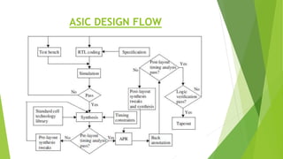
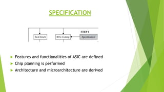
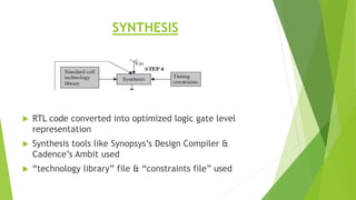
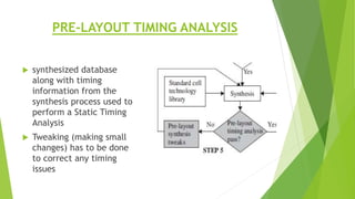
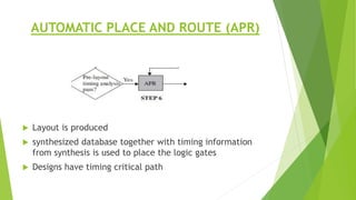
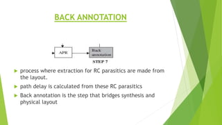
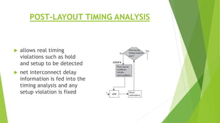
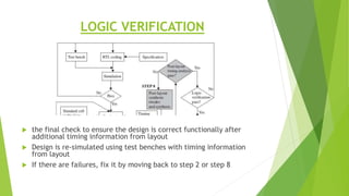
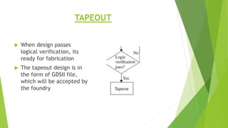


This document outlines the typical ASIC design flow process. It begins with specification where the features and functionalities of the ASIC are defined. This is followed by RTL coding to develop the logic functionality in a hardware description language. Simulation and synthesis then convert the RTL into a gate-level netlist. Pre-layout timing analysis checks for timing issues. Then automatic place and route lays out the design on the chip. Back annotation adds layout parasitic information. Post-layout timing analysis checks for real timing violations. Logic verification confirms correct functionality. The final tapeout step sends the design for fabrication if all checks pass.