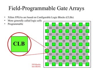
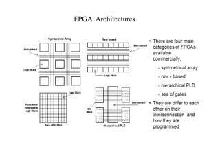
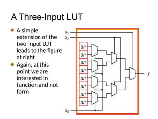
What is anFPGA?
• An FPGA is a general-purpose, multi-level
programmable logic device that is customized in the
package by the end users.
• FPGAs are composed of blocks of logic connected with
programmable interconnect.
• The programmable interconnect between blocks allows
users to implement multi-level logic, removing many of the
size limitations of the PLD-derived two-level logic
structure.
• This extensible architecture can currently support thousands
of gates of logic at system speeds in the tens of megahertz.
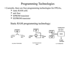
Programming Technologies
• Currently,there are four programming technologies for FPGAs,
static RAM cells
anti fuse
EPROM transistor
EEPROM transistor
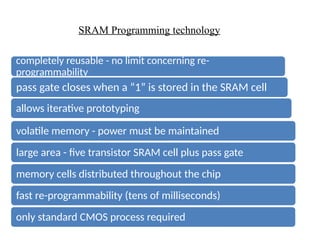
Static RAM programming technology:
8.
SRAM Programming technology
completelyreusable - no limit concerning re-
programmability
pass gate closes when a “1” is stored in the SRAM cell
allows iterative prototyping
volatile memory - power must be maintained
large area - five transistor SRAM cell plus pass gate
memory cells distributed throughout the chip
fast re-programmability (tens of milliseconds)
only standard CMOS process required
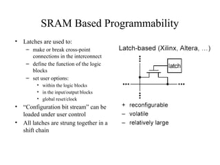
9.
SRAM Based Programmability
•Latches are used to:
– make or break cross-point
connections in the interconnect
– define the function of the logic
blocks
– set user options:
• within the logic blocks
• in the input/output blocks
• global reset/clock
• “Configuration bit stream” can be
loaded under user control
• All latches are strung together in a
shift chain
10.
Anti-fuse Programming
• Ananti-fuse is the opposite of normal fuse.
• Anti-fuse are made with a modified CMOS process having an extra step
• This step creates a very thin insulating layer which separates two
conducting layers
• That thin insulating layer is fused by applying a high voltage across the
conducting layer
• Such high voltage can be destructive for CMOS logic circuit
• Non-volatile (Permanent)
• Requires extra programming circuitry, including a programming
transistor
11.
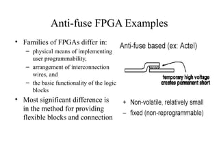
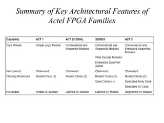
Anti-fuse FPGA Examples
•Families of FPGAs differ in:
– physical means of implementing
user programmability,
– arrangement of interconnection
wires, and
– the basic functionality of the logic
blocks
• Most significant difference is
in the method for providing
flexible blocks and connection
12.
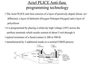
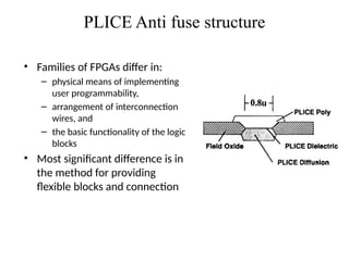
Actel PLICE Anti-fuse
programmingtechnology
• The Actel PLICE anti-fuse consists of a layer of positively doped silicon (n+
diffusion), a layer of dielectric (Oxygen-Nitrogen-Oxygen) and a layer of
polysilicon
• it is programmed by placing a relatively high voltage (18V) across the
antifuse terminals which results current of about 5 mA through it
• typical resistance of a fused contact is 300 to 500 Ω
• manufactured by 3 additional masks to a normal CMOS process
13.
Quick logic ViaLink Anti fuse
programming technology
• amorphous silicon is used as an insulating layer
• direct metal to metal contact results path resistance below 50 Ω
• 10 V terminal voltage is required to fuse the amorphous silicon
14.
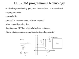
EEPROM programming technology
•static charge on floating gate turns the transistor permanently off
• re-programmable
• non-volatile
• external permanent memory is not required
• slow re-configuration time
• floating-gate FET has relatively high on resistance
• higher static power consumption due to pull up resistor
15.
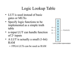
Logic Lookup Table
•LUT is used instead of basic
gates or MUXs
• Specify logic functions to be
implemented as a simple truth
table
• n-input LUT can handle function
of 2n
inputs
• A LUT is actually a small (1-bit)
RAM
– FPGA LUTs can be used as RAM
16.
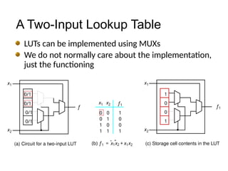
(a) Circuit fora two-input LUT
x1
x2
f
0/1
0/1
0/1
0
0
1
1
0
1
0
1
1
0
0
1
x1 x2
(b) f1 x1x2 x1x2
+
=
f1
(c) Storage cell contents in the LUT
x1
x2
1
0
0
1
f1
A Two-Input Lookup Table
LUTs can be implemented using MUXs
We do not normally care about the implementation,
just the functioning
0/1
Out
D Q
Clock
Select
Flip-flop
In 1
In2
In 3
LUT
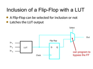
Inclusion of a Flip-Flop with a LUT
A Flip-Flop can be selected for inclusion or not
Latches the LUT output
can program to
bypass the FF
19.
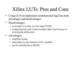
Xilinx LUTs: Prosand Cons
• Using LUTs to implement combinational logic has both
advantages and disadvantages
• Disadvantages:
– an inverter is as slow as a five input NAND
– routing between cells is more complex than Actel because of
coarse-grain architecture
• Advantages:
– simplifies timing
– same delay for any function of five variables
– can be used directly as SRAM
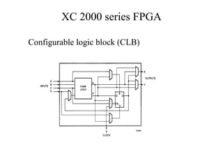
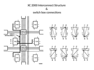
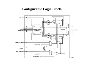
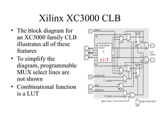
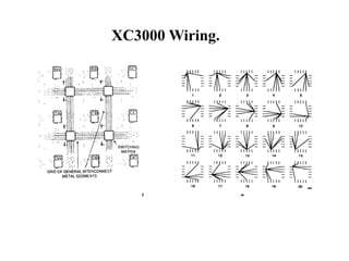
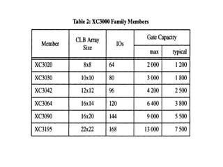
Xilinx XC3000 CLB
•The block diagram for
an XC3000 family CLB
illustrates all of these
features
• To simplify the
diagram, programmable
MUX select lines are
not shown
• Combinational function
is a LUT
LUT
27.
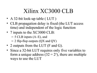
Xilinx XC3000 CLB
•A 32-bit look-up table ( LUT )
• CLB propagation delay is fixed (the LUT access
time) and independent of the logic function
• 7 inputs to the XC3000 CLB:
– 5 CLB inputs (A–E), and
– 2 flip-flop outputs (QX and QY)
• 2 outputs from the LUT (F and G).
• Since a 32-bit LUT requires only five variables to
form a unique address (32 = 25
), there are multiple
ways to use the LUT
28.
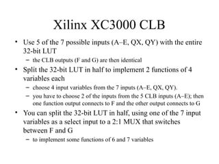
Xilinx XC3000 CLB
•Use 5 of the 7 possible inputs (A–E, QX, QY) with the entire
32-bit LUT
– the CLB outputs (F and G) are then identical
• Split the 32-bit LUT in half to implement 2 functions of 4
variables each
– choose 4 input variables from the 7 inputs (A–E, QX, QY).
– you have to choose 2 of the inputs from the 5 CLB inputs (A–E); then
one function output connects to F and the other output connects to G
• You can split the 32-bit LUT in half, using one of the 7 input
variables as a select input to a 2:1 MUX that switches
between F and G
– to implement some functions of 6 and 7 variables
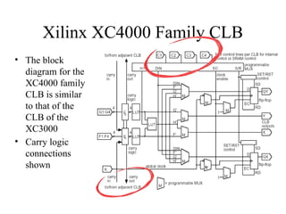
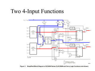
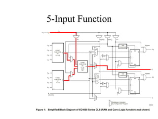
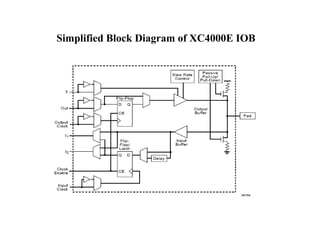
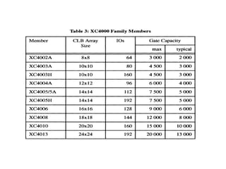
Xilinx XC4000 FamilyCLB
• The block
diagram for the
XC4000 family
CLB is similar
to that of the
CLB of the
XC3000
• Carry logic
connections
shown
34.
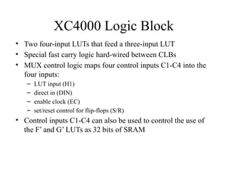
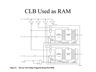
XC4000 Logic Block
•Two four-input LUTs that feed a three-input LUT
• Special fast carry logic hard-wired between CLBs
• MUX control logic maps four control inputs C1-C4 into the
four inputs:
– LUT input (H1)
– direct in (DIN)
– enable clock (EC)
– set/reset control for flip-flops (S/R)
• Control inputs C1-C4 can also be used to control the use of
the F’ and G’ LUTs as 32 bits of SRAM
PLICE Anti fusestructure
• Families of FPGAs differ in:
– physical means of implementing
user programmability,
– arrangement of interconnection
wires, and
– the basic functionality of the logic
blocks
• Most significant difference is in
the method for providing
flexible blocks and connection
45.
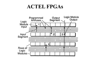
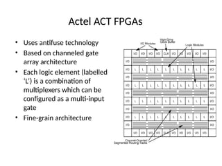
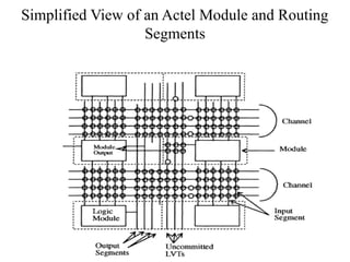
Actel ACT FPGAs
•Uses antifuse technology
• Based on channeled gate
array architecture
• Each logic element (labelled
‘L’) is a combination of
multiplexers which can be
configured as a multi-input
gate
• Fine-grain architecture
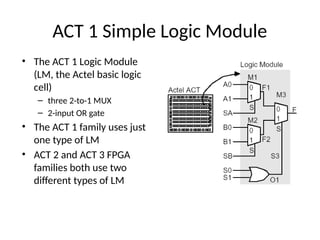
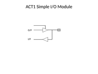
ACT 1 SimpleLogic Module
• The ACT 1 Logic Module
(LM, the Actel basic logic
cell)
– three 2-to-1 MUX
– 2-input OR gate
• The ACT 1 family uses just
one type of LM
• ACT 2 and ACT 3 FPGA
families both use two
different types of LM
48.
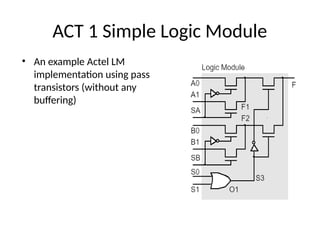
ACT 1 SimpleLogic Module
• An example Actel LM
implementation using pass
transistors (without any
buffering)
49.
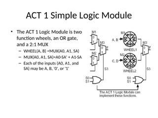
ACT 1 SimpleLogic Module
• The ACT 1 Logic Module is two
function wheels, an OR gate,
and a 2:1 MUX
– WHEEL(A, B) =MUX(A0, A1, SA)
– MUX(A0, A1, SA)=A0·SA' + A1·SA
– Each of the inputs (A0, A1, and
SA) may be A, B, '0', or '1'
50.
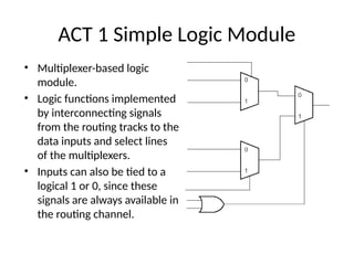
ACT 1 SimpleLogic Module
• Multiplexer-based logic
module.
• Logic functions implemented
by interconnecting signals
from the routing tracks to the
data inputs and select lines
of the multiplexers.
• Inputs can also be tied to a
logical 1 or 0, since these
signals are always available in
the routing channel.
51.
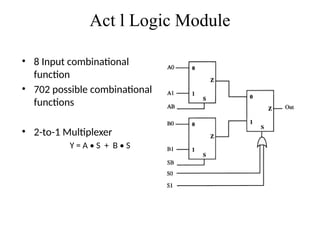
Act l LogicModule
• 8 Input combinational
function
• 702 possible combinational
functions
• 2-to-1 Multiplexer
Y = A • S + B • S
52.
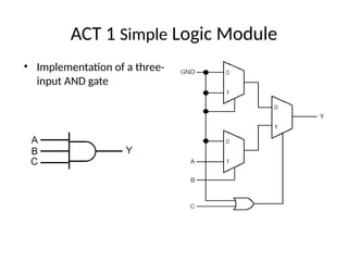
ACT 1 SimpleLogic Module
• Implementation of a three-
input AND gate
53.
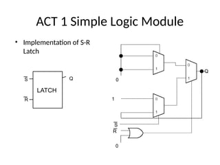
ACT 1 SimpleLogic Module
0
0
1
Q
S
R
• Implementation of S-R
Latch
S
R
Q
LATCH
54.
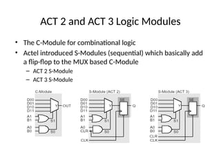
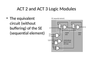
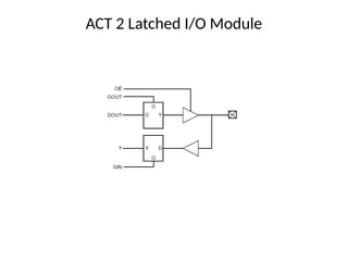
ACT 2 andACT 3 Logic Modules
• The C-Module for combinational logic
• Actel introduced S-Modules (sequential) which basically add
a flip-flop to the MUX based C-Module
– ACT 2 S-Module
– ACT 3 S-Module
55.
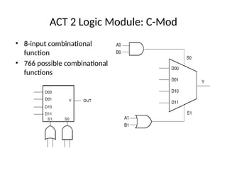
ACT 2 LogicModule: C-Mod
• 8-input combinational
function
• 766 possible combinational
functions
56.
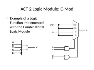
ACT 2 LogicModule: C-Mod
• Example of a Logic
Function Implemented
with the Combinatorial
Logic Module
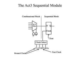
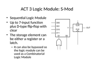
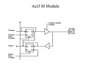
ACT 3 LogicModule: S-Mod
• Sequential Logic Module
• Up to 7-input function
plus D-type flip-flop with
clear
• The storage element can
be either a register or a
latch.
– It can also be bypassed so
the logic module can be
used as a Combinatorial
Logic Module
60.
ACT 2 andACT 3 Logic Modules
• The equivalent
circuit (without
buffering) of the SE
(sequential element)
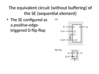
61.
The equivalent circuit(without buffering) of
the SE (sequential element)
• The SE configured as
a positive-edge-
triggered D flip-flop
62.
Actel Logic ModuleAnalysis
• Actel uses a fine-grain architecture which allows you to use
almost all of the FPGA
• Synthesis can map logic efficiently to a fine-grain
architecture
• Physical symmetry simplifies place-and-route (swapping
equivalent pins on opposite sides of the LM to ease routing)
• Matched to small antifuse programming technology
• LMs balance efficiency of implementation and efficiency of
utilization
• A simple LM reduces performance, but allows fast and
robust place-and-route
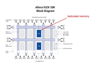
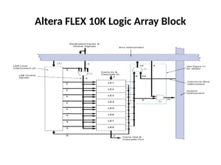
• Logic ArrayBlock
• Each LAB consists of eight LEs, their associated
carry and cascade chains, LAB control signals,
and the LAB local interconnect.
• The LAB provides the coarse-grained structure
to the Altera architecture
Altera FLEX 10K Logic Array Block