Downloaded 253 times


![Physical Structure of MOS FETS
NMOS
PMOS
Er. Vikram Kumar Kamboj
[Adapted from Principles of CMOS VLSI Design by Weste & Eshraghian]](https://image.slidesharecdn.com/14827mosfet-141214020912-conversion-gate02/75/14827-mosfet-10-2048.jpg)

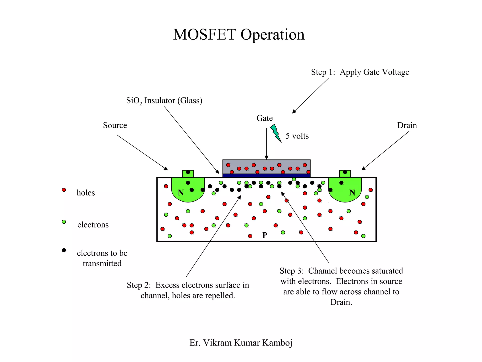


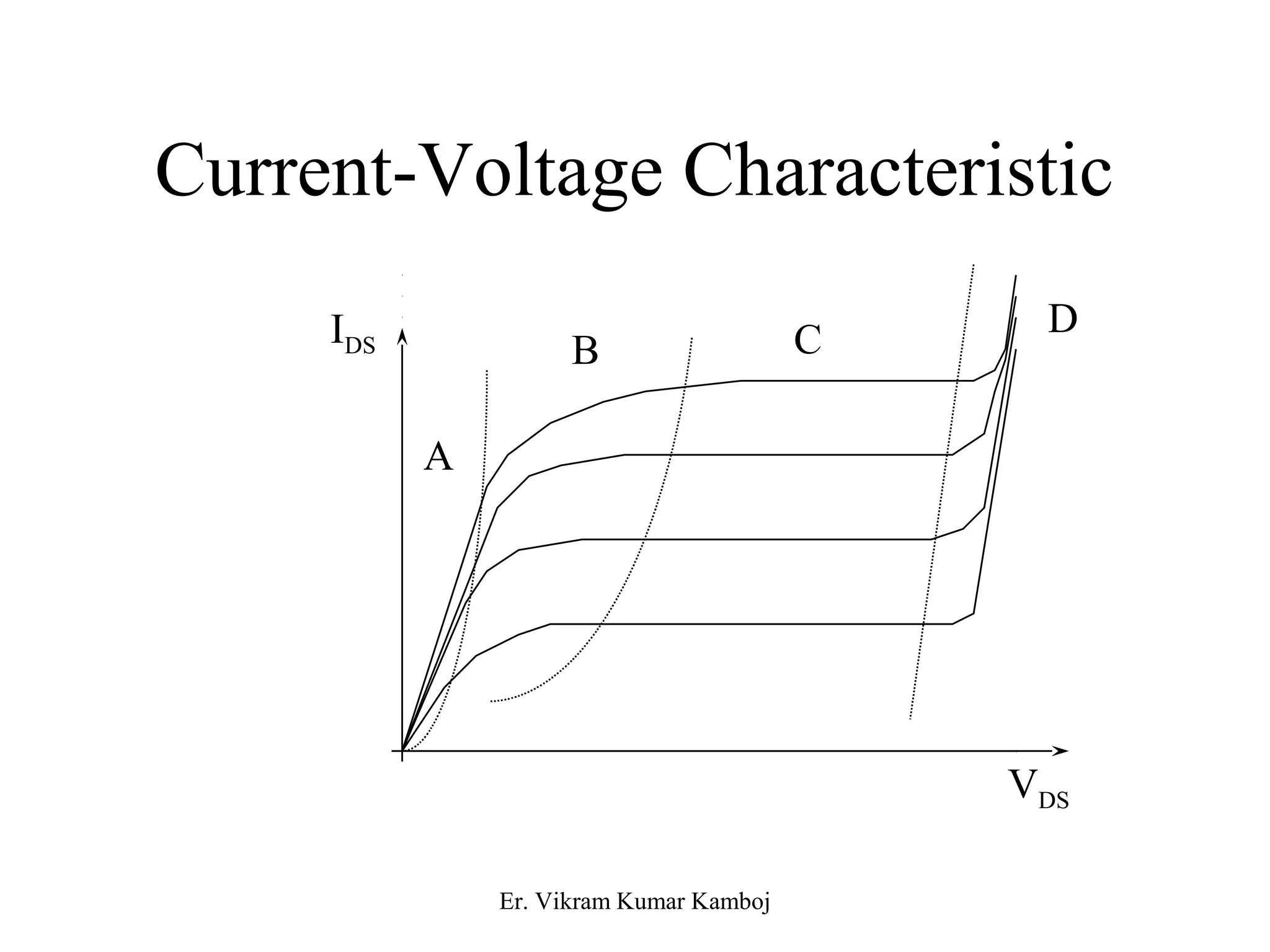


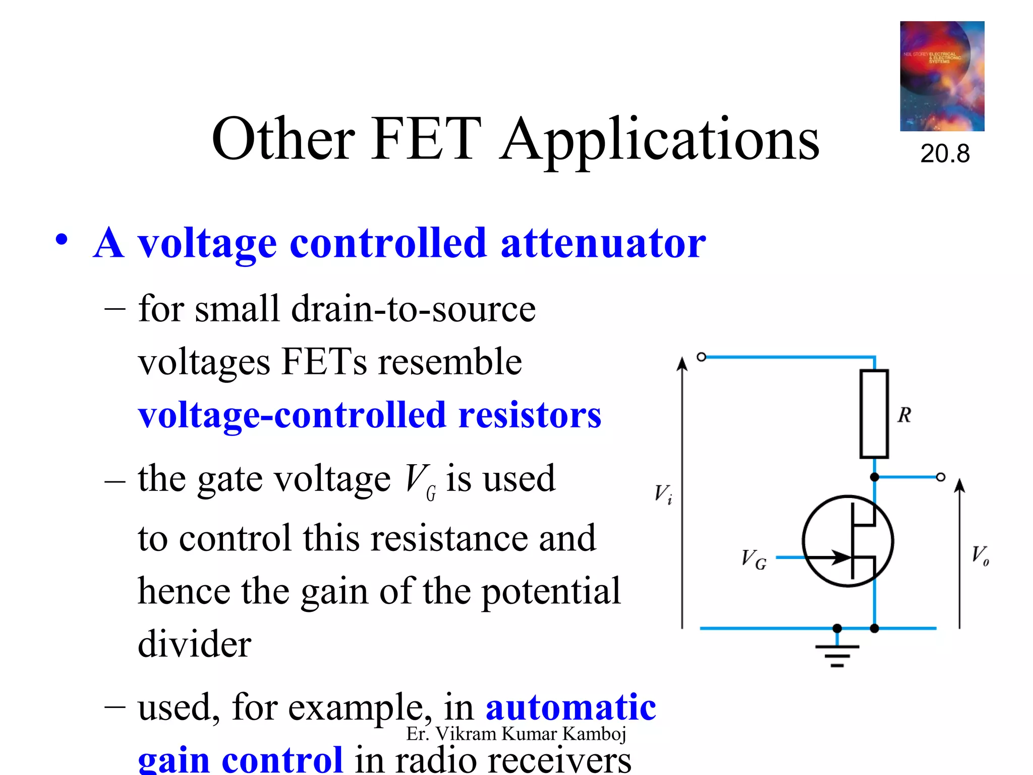


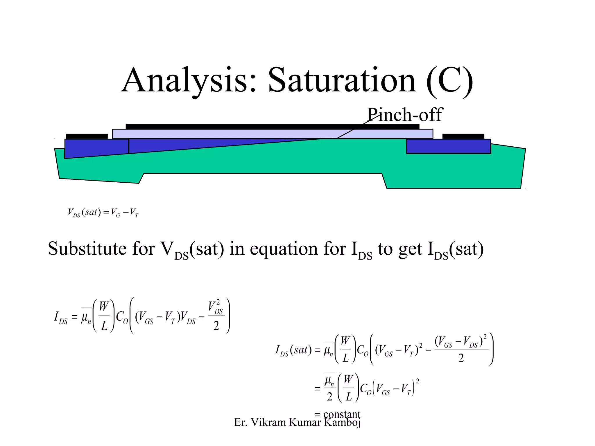


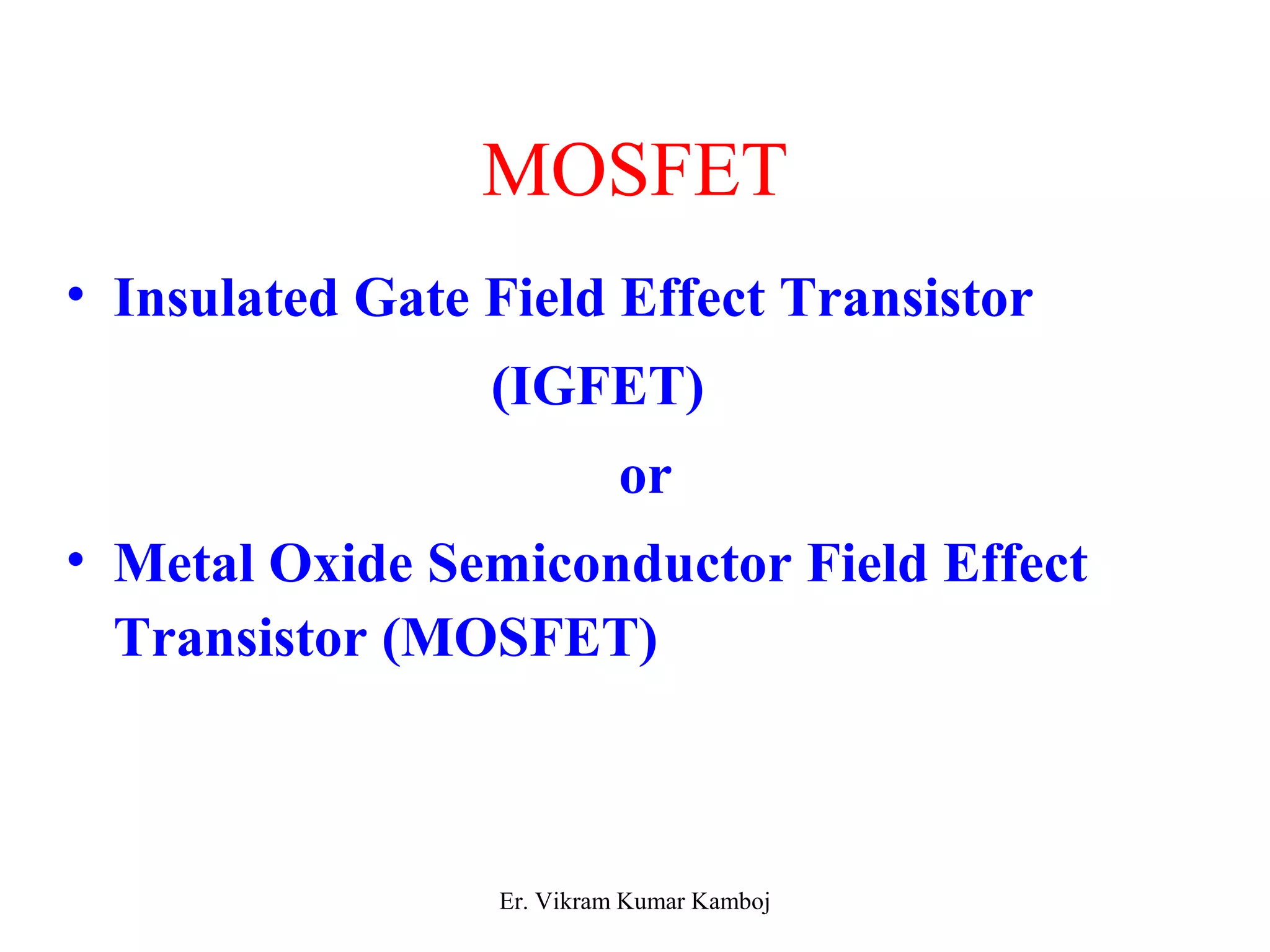
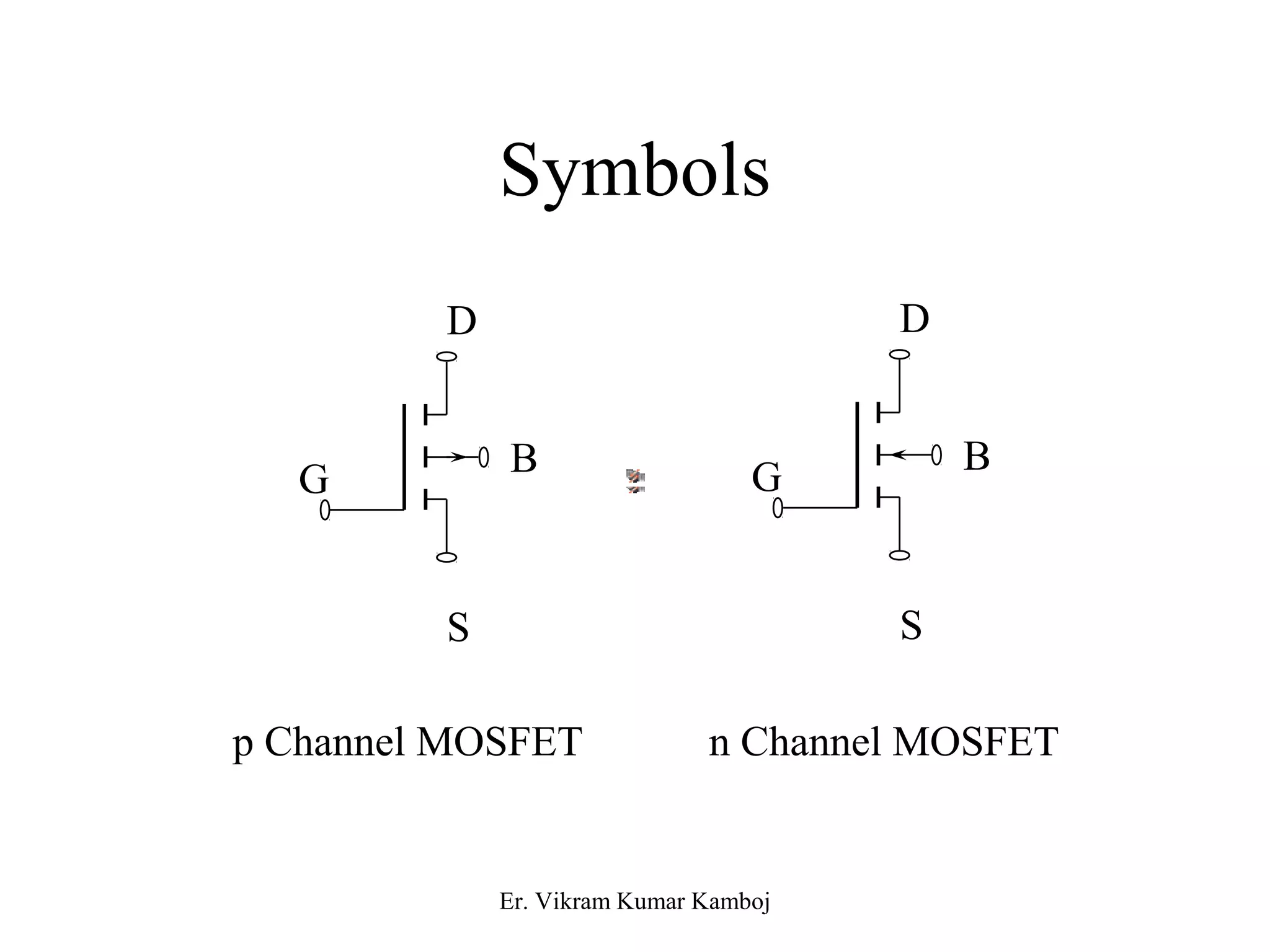
The document discusses the metal-oxide-semiconductor field-effect transistor (MOSFET). It describes the basic structure of the MOSFET, including the source, gate, and drain terminals. It also discusses the different types of MOSFETs, such as n-channel and p-channel MOSFETs, as well as depletion and enhancement MOSFETs. The key characteristics of MOSFETs are summarized, including the different regions of operation depending on the voltages applied to the gate, source, and drain terminals. Common applications of MOSFETs in analog and digital circuits are also outlined.


![Seller Deck - Presentation [Concert L2].PPTX](https://cdn.slidesharecdn.com/ss_thumbnails/sellerdeck-presentationconcertl2-251219171156-24982daf-thumbnail.jpg?width=640&height=640&fit=bounds)


