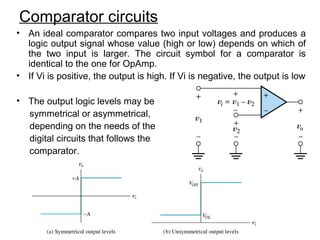
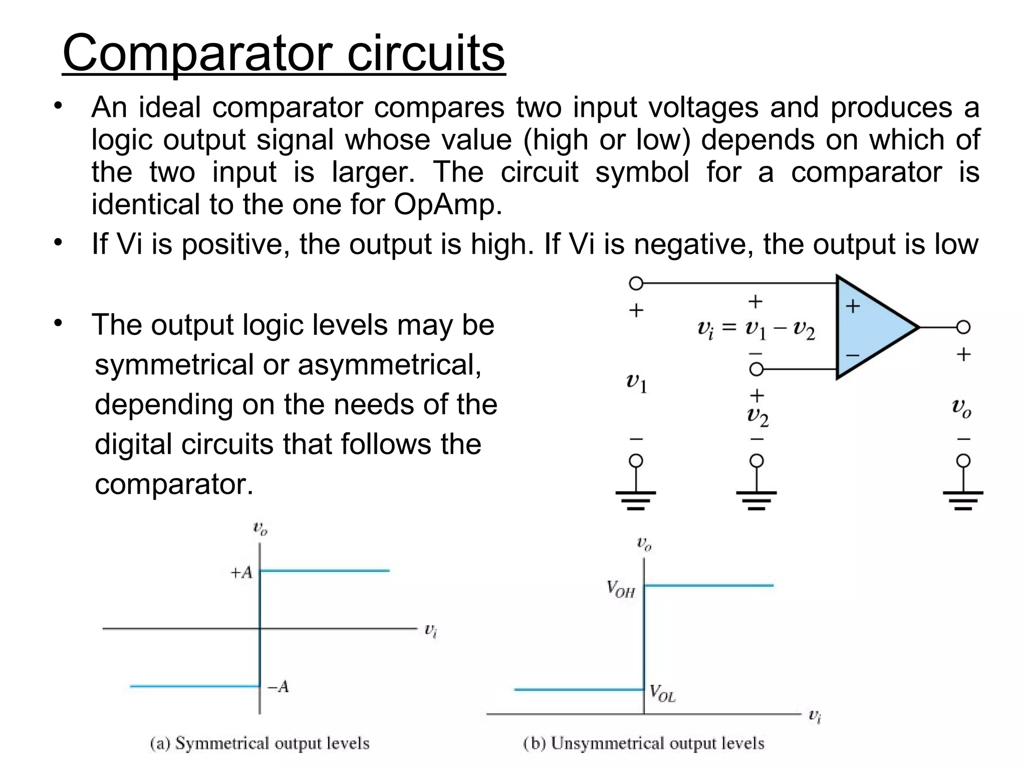
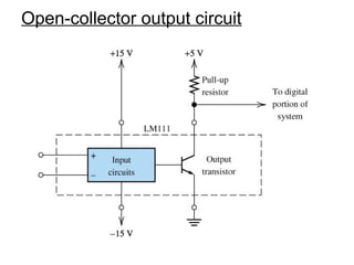
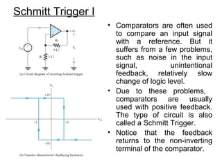
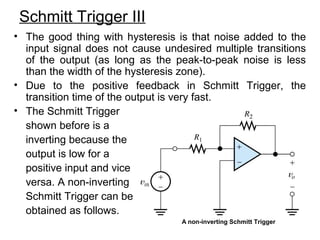
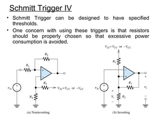
Comparator circuits
• An ideal comparator compares two input voltages and produces a
logic output signal whose value (high or low) depends on which of
the two input is larger. The circuit symbol for a comparator is
identical to the one for OpAmp.
• If Vi is positive, the output is high. If Vi is negative, the output is low
• The output logic levels may be
symmetrical or asymmetrical,
depending on the needs of the
digital circuits that follows the
comparator.
Comparator circuits
• Real comparator circuits do not display an abrupt
transition in the output.
• Voltage gain is extremely high in the transition region.
• Internal circuitry of the an integrated comparator is similar
to that of an OpAmp. One important difference is that
frequency compensation is not needed for comparator
because it is not operated in negative feedback.
• So, roughly, OpAmp can be used as a comparator circuit,
but not vice versa due to frequency compensation.
• Comparator is usually designed to have small transition
region and small propagation delay for output signal in
response to inputs.
• Comparator also suffer from non-idealities, such as bias
current, offset current and offset voltage.
Open-collector output
• Comparators are often used as the interface between
analog and digital circuits, since it converts analog signal
into logic levels.
• Power supply for analog signal in many systems are 10 to
15V. But power supply for digital signal is 1.8 to 5V.
• Suppose for digital signal, 0V stands for logic 0 and 5V for
logic 1, then a comparator needs to produce an output of
0V and 5V with input and internal signal at 0 to 15V. An
open-collector output stage are very useful in the case.
• For example, in open-collector output stage, the output
terminals are the emitter and collector of a NPN transistor.
If the output is intended to be low (0), the transistor is
driven to saturation so the output voltage is about 0.2V
(saturation voltage of BJT). On the other hand, if the
output should be high, the output transistor is cutoff and
current does flow through transistor, resulting about 5V
output
Open-collector output circuit
Schmitt Trigger I
• Comparators are often used
to compare an input signal
with a reference. But it
suffers from a few problems,
such as noise in the input
signal, unintentional
feedback, relatively slow
change of logic level.
• Due to these problems,
comparators are usually
used with positive feedback.
The type of circuit is also
called a Schmitt Trigger.
• Notice that the feedback
returns to the non-inverting
terminal of the comparator.
Schmitt Trigger II
• One interesting thing about Schmitt Trigger is the transfer
characteristic.
• Suppose the output level are +10V or -10V. If the input
voltage is negative and of sufficient magnitude, the
comparator output is +10V (high). Because of the feedback
path, the voltage at non-inverting input is +1V, thus the
input voltage has to increase to +1V before the output
switches to -10V.
• On the other hand, if the output is -10V (low), the voltage at
non-inverting input is -1V, so the input must decrease to
-1V before the output switches to +10V (high).
• For input voltage between -1V and 1V, the output could be
either high or low, depending on the past history of the
input voltage.
• The difference between the switching thresholds for an
increasing input and decreasing input is called hysteresis.
Noise Suppression using
Schmitt Trigger
Vin
t0
VM−
VM+
t
Vout
t0 + tp t
Schmitt Trigger III
• The good thing with hysteresis is that noise added to the
input signal does not cause undesired multiple transitions
of the output (as long as the peak-to-peak noise is less
than the width of the hysteresis zone).
• Due to the positive feedback in Schmitt Trigger, the
transition time of the output is very fast.
• The Schmitt Trigger
shown before is a
inverting because the
output is low for a
positive input and vice
versa. A non-inverting
Schmitt Trigger can be
obtained as follows.
A non-inverting Schmitt Trigger
Schmitt Trigger IV
• Schmitt Trigger can be designed to have specified
thresholds.
• One concern with using these triggers is that resistors
should be properly chosen so that excessive power
consumption is avoided.
Schmitt Trigger IV
• Schmitt Trigger can be designed to have specified
thresholds.
• One concern with using these triggers is that resistors
should be properly chosen so that excessive power
consumption is avoided.

Schmitt trigger circuit

  • 1.
    Comparator circuits • Anideal comparator compares two input voltages and produces a logic output signal whose value (high or low) depends on which of the two input is larger. The circuit symbol for a comparator is identical to the one for OpAmp. • If Vi is positive, the output is high. If Vi is negative, the output is low • The output logic levels may be symmetrical or asymmetrical, depending on the needs of the digital circuits that follows the comparator.
  • 2.
    Comparator circuits • Realcomparator circuits do not display an abrupt transition in the output. • Voltage gain is extremely high in the transition region. • Internal circuitry of the an integrated comparator is similar to that of an OpAmp. One important difference is that frequency compensation is not needed for comparator because it is not operated in negative feedback. • So, roughly, OpAmp can be used as a comparator circuit, but not vice versa due to frequency compensation. • Comparator is usually designed to have small transition region and small propagation delay for output signal in response to inputs. • Comparator also suffer from non-idealities, such as bias current, offset current and offset voltage.
  • 3.
    Open-collector output • Comparatorsare often used as the interface between analog and digital circuits, since it converts analog signal into logic levels. • Power supply for analog signal in many systems are 10 to 15V. But power supply for digital signal is 1.8 to 5V. • Suppose for digital signal, 0V stands for logic 0 and 5V for logic 1, then a comparator needs to produce an output of 0V and 5V with input and internal signal at 0 to 15V. An open-collector output stage are very useful in the case. • For example, in open-collector output stage, the output terminals are the emitter and collector of a NPN transistor. If the output is intended to be low (0), the transistor is driven to saturation so the output voltage is about 0.2V (saturation voltage of BJT). On the other hand, if the output should be high, the output transistor is cutoff and current does flow through transistor, resulting about 5V output
  • 4.
  • 5.
    Schmitt Trigger I •Comparators are often used to compare an input signal with a reference. But it suffers from a few problems, such as noise in the input signal, unintentional feedback, relatively slow change of logic level. • Due to these problems, comparators are usually used with positive feedback. The type of circuit is also called a Schmitt Trigger. • Notice that the feedback returns to the non-inverting terminal of the comparator.
  • 6.
    Schmitt Trigger II •One interesting thing about Schmitt Trigger is the transfer characteristic. • Suppose the output level are +10V or -10V. If the input voltage is negative and of sufficient magnitude, the comparator output is +10V (high). Because of the feedback path, the voltage at non-inverting input is +1V, thus the input voltage has to increase to +1V before the output switches to -10V. • On the other hand, if the output is -10V (low), the voltage at non-inverting input is -1V, so the input must decrease to -1V before the output switches to +10V (high). • For input voltage between -1V and 1V, the output could be either high or low, depending on the past history of the input voltage. • The difference between the switching thresholds for an increasing input and decreasing input is called hysteresis.
  • 7.
    Noise Suppression using SchmittTrigger Vin t0 VM− VM+ t Vout t0 + tp t
  • 8.
    Schmitt Trigger III •The good thing with hysteresis is that noise added to the input signal does not cause undesired multiple transitions of the output (as long as the peak-to-peak noise is less than the width of the hysteresis zone). • Due to the positive feedback in Schmitt Trigger, the transition time of the output is very fast. • The Schmitt Trigger shown before is a inverting because the output is low for a positive input and vice versa. A non-inverting Schmitt Trigger can be obtained as follows. A non-inverting Schmitt Trigger
  • 9.
    Schmitt Trigger IV •Schmitt Trigger can be designed to have specified thresholds. • One concern with using these triggers is that resistors should be properly chosen so that excessive power consumption is avoided.
  • 10.
    Schmitt Trigger IV •Schmitt Trigger can be designed to have specified thresholds. • One concern with using these triggers is that resistors should be properly chosen so that excessive power consumption is avoided.