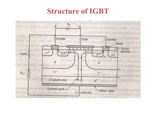
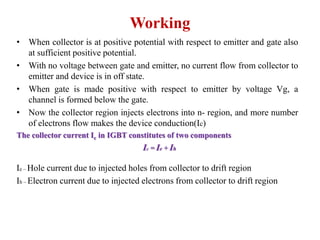
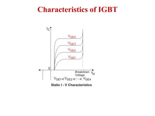
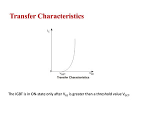
IGBT
(Insulated Gate Bipolar
Transistor)
Prepared by,
Mr. A. Johny Renoald M.E., Ph.D.,
Symbol and Structure
• The insulated gate bipolar transistor is a three terminal
semiconductor device
• Gate, Emitter and Collector
• Emitter and Collector-Associated with a conductance path
• Gate terminal is associated with its control
• IGBT has MOSFET like input characteristics and Power BJT like output
characteristics
• So its called as Voltage Controlled Device
Structure of IGBT
Working
• When collector is at positive potential with respect to emitter and gate also
at sufficient positive potential.
• With no voltage between gate and emitter, no current flow from collector to
emitter and device is in off state.
• When gate is made positive with respect to emitter by voltage Vg, a
channel is formed below the gate.
• Now the collector region injects electrons into n- region, and more number
of electrons flow makes the device conduction(Ic)
The collector current Ic in IGBT constitutes of two components
Ic = Ie + Ih
Ie – Hole current due to injected holes from collector to drift region
Ih – Electron current due to injected electrons from collector to drift region
Characteristics of IGBT
Transfer Characteristics
The IGBT is in ON-state only after VGE is greater than a threshold value VGET.
Switching Characteristics of IGBT
Turn on time ton is composed of two components as usual, delay time (tdn) and rise time (tr)
Delay Time
Delay time is defined as the time in which collector current rises from leakage current
ICE to 0.1 IC (final collector current) and collector emitter voltage falls from VCE to 0.9VCE
Rise Time
Rise time is defined as the time in which collector current rises from 0.1 IC to IC and
collector emitter voltage falls from 0.9VCE to 0.1 VCE.
The turn off time toff consists of three components, delay time (tdf), initial fall time (tf1) and
final fall time (tf2)
Turn off Delay Time
Delay time is defined as time when collector current falls from IC to 0.9 IC and VCE begins
to rise
Initial fall time
Initial fall time is the time during which collector current falls from 0.9 IC to 0.2 IC and
collector emitter voltage rises to 0.1 VCE
Final fall time
The final fall time is defined as time during which collector current falls from 0.2 IC to 0.1
IC and 0.1VCE rises to final value VCE
Series and Parallel Connection of SCR
• Nowadays, SCRs are available of ratings up to 10 KV and 3 KA. But
sometimes we face demand, more than these ratings.
• In this case combination of more than one SCRs is used.
• Series connection of SCRs meets high voltage demand and parallel
connection of SCRs meets high current demand.
• These series and parallel connection of SCR or Thyristor will work
efficiently if all SCRs are fully utilized.
• Although all SCRs in a string are of same rating, their V-I characteristics
differ from one another. This leads to unequal voltage or current division
among them.
• Hence every SCR is not fully utilized. So the efficiency of string is always
less than 100% according to the given expression
Series Operation of SCR
• When the operating voltage is more than the rating of one SCR the multiple
SCRs of same ratings are used in series
• SCR’s having same rating, may have different I-V characteristic, so
unequal voltage division is takes place
• For example if two SCRs in series that is capable of blocking 5 KV
individually, then the string should block 10 KV. But practically this does
not happen.
• Voltage across SCR1 is V1 but that across SCR2 is V2
• V2 is much less than V1. So, SCR2 is not fully utilized. Hence the string can
block V1 + V2 = 8 KV, rather than 10 KV
• The string efficiency = 80%
• To improve the efficiency a resistor in parallel with every SCR is used.
• The value of these resistances are such that the equivalent resistance of
each SCR and resistor pair will be same.
• Ensures equal voltage division across each SCR
One value of resistance to get optimum result which is given by
n = no. of SCR in the string
V bm = Voltage blocked by the SCR having minimum leakage current.
Δ Ib = Difference between maximum and minimum leakage current flowing through SCRs
Vs = Voltage across the string
Parallel Operation of SCR
Static current sharing
• Resistors are used in case of static current sharing. When resistances are
used in series, the losses may become high.
Dynamic current sharing
• For dynamic current sharing, inductors are also used in addition to the
resistors.
• In case of inductors (magnetically coupled), if current through the thyristor
T1 increases, an opposite polarity voltage would be induced (as of series
coil of T1) in the series coil of thyristor T2
Thyristor Protection or SCR Protection
• Protection of a device is an important aspect for its reliable and efficient
operation
• SCR may face different types of threats during its operation due to over
voltages, over currents etc.
• Different types of thyristor protection schemes available for satisfactory
operation
1.Over voltage protection
2. Over current protection
3. High dv/dt protection
4. Thermal protection
Over Voltage Protection
• Most important protection scheme w. r. t. others as thyristors are very
sensitive to over voltages.
• Maximum time thyristor failures happen due to over-voltage
Internal Over-Voltages
• After commutation of a thyristor reverse recovery current decays abruptly
that can exceed the rated break-over voltage and the device may be
damaged
External Over-Voltages
• Due to various reasons in the supply line like lightning, surge conditions
(abnormal voltage spike) etc
• External over voltage may cause different types of problem in thyristor
operation like increase in leakage current, permanent breakdown of
junctions, unwanted turn-on of devices etc.
Over Current Protection
• Over current mainly occurs due to different types of faults in the circuit
• Due to over current loss will increase and high generation of heat may take
place that can exceed the permissible limit and burn the device
Protective Measures
• SCR can be protected from over current by using CB and fast acting
current limiting fuses
• CB are used for protection of thyristor against continuous overloads or
against surge currents of long duration as a CB has long tripping time
High dv/dt Protection
• When a thyristor is in forward blocking state then only J2 junction is
reverse biased which acts as a capacitor having constant capacitance value
Cj (junction capacitance)
• Current through capacitor follows the relation
• Hence leakage current through the J2 junction which is nothing but the
leakage current through the device will increase which damaged the device
and it should be avoided
Thermal or Temperature Protection
• With the increase in the temperature of the junction, insulation may get
failed.
• So we have to take proper measures to limit the temperature rise

IGBT

  • 1.
    IGBT (Insulated Gate Bipolar Transistor) Preparedby, Mr. A. Johny Renoald M.E., Ph.D.,
  • 2.
    Symbol and Structure •The insulated gate bipolar transistor is a three terminal semiconductor device • Gate, Emitter and Collector • Emitter and Collector-Associated with a conductance path • Gate terminal is associated with its control
  • 3.
    • IGBT hasMOSFET like input characteristics and Power BJT like output characteristics • So its called as Voltage Controlled Device
  • 4.
  • 5.
    Working • When collectoris at positive potential with respect to emitter and gate also at sufficient positive potential. • With no voltage between gate and emitter, no current flow from collector to emitter and device is in off state. • When gate is made positive with respect to emitter by voltage Vg, a channel is formed below the gate. • Now the collector region injects electrons into n- region, and more number of electrons flow makes the device conduction(Ic) The collector current Ic in IGBT constitutes of two components Ic = Ie + Ih Ie – Hole current due to injected holes from collector to drift region Ih – Electron current due to injected electrons from collector to drift region
  • 6.
  • 7.
    Transfer Characteristics The IGBTis in ON-state only after VGE is greater than a threshold value VGET.
  • 8.
  • 9.
    Turn on timeton is composed of two components as usual, delay time (tdn) and rise time (tr) Delay Time Delay time is defined as the time in which collector current rises from leakage current ICE to 0.1 IC (final collector current) and collector emitter voltage falls from VCE to 0.9VCE Rise Time Rise time is defined as the time in which collector current rises from 0.1 IC to IC and collector emitter voltage falls from 0.9VCE to 0.1 VCE. The turn off time toff consists of three components, delay time (tdf), initial fall time (tf1) and final fall time (tf2) Turn off Delay Time Delay time is defined as time when collector current falls from IC to 0.9 IC and VCE begins to rise Initial fall time Initial fall time is the time during which collector current falls from 0.9 IC to 0.2 IC and collector emitter voltage rises to 0.1 VCE Final fall time The final fall time is defined as time during which collector current falls from 0.2 IC to 0.1 IC and 0.1VCE rises to final value VCE
  • 10.
    Series and ParallelConnection of SCR • Nowadays, SCRs are available of ratings up to 10 KV and 3 KA. But sometimes we face demand, more than these ratings. • In this case combination of more than one SCRs is used. • Series connection of SCRs meets high voltage demand and parallel connection of SCRs meets high current demand. • These series and parallel connection of SCR or Thyristor will work efficiently if all SCRs are fully utilized. • Although all SCRs in a string are of same rating, their V-I characteristics differ from one another. This leads to unequal voltage or current division among them. • Hence every SCR is not fully utilized. So the efficiency of string is always less than 100% according to the given expression
  • 11.
    Series Operation ofSCR • When the operating voltage is more than the rating of one SCR the multiple SCRs of same ratings are used in series • SCR’s having same rating, may have different I-V characteristic, so unequal voltage division is takes place • For example if two SCRs in series that is capable of blocking 5 KV individually, then the string should block 10 KV. But practically this does not happen.
  • 12.
    • Voltage acrossSCR1 is V1 but that across SCR2 is V2 • V2 is much less than V1. So, SCR2 is not fully utilized. Hence the string can block V1 + V2 = 8 KV, rather than 10 KV • The string efficiency = 80% • To improve the efficiency a resistor in parallel with every SCR is used. • The value of these resistances are such that the equivalent resistance of each SCR and resistor pair will be same. • Ensures equal voltage division across each SCR One value of resistance to get optimum result which is given by n = no. of SCR in the string V bm = Voltage blocked by the SCR having minimum leakage current. Δ Ib = Difference between maximum and minimum leakage current flowing through SCRs Vs = Voltage across the string
  • 13.
  • 14.
    Static current sharing •Resistors are used in case of static current sharing. When resistances are used in series, the losses may become high. Dynamic current sharing • For dynamic current sharing, inductors are also used in addition to the resistors. • In case of inductors (magnetically coupled), if current through the thyristor T1 increases, an opposite polarity voltage would be induced (as of series coil of T1) in the series coil of thyristor T2
  • 15.
    Thyristor Protection orSCR Protection • Protection of a device is an important aspect for its reliable and efficient operation • SCR may face different types of threats during its operation due to over voltages, over currents etc. • Different types of thyristor protection schemes available for satisfactory operation 1.Over voltage protection 2. Over current protection 3. High dv/dt protection 4. Thermal protection
  • 16.
    Over Voltage Protection •Most important protection scheme w. r. t. others as thyristors are very sensitive to over voltages. • Maximum time thyristor failures happen due to over-voltage Internal Over-Voltages • After commutation of a thyristor reverse recovery current decays abruptly that can exceed the rated break-over voltage and the device may be damaged External Over-Voltages • Due to various reasons in the supply line like lightning, surge conditions (abnormal voltage spike) etc • External over voltage may cause different types of problem in thyristor operation like increase in leakage current, permanent breakdown of junctions, unwanted turn-on of devices etc.
  • 17.
    Over Current Protection •Over current mainly occurs due to different types of faults in the circuit • Due to over current loss will increase and high generation of heat may take place that can exceed the permissible limit and burn the device Protective Measures • SCR can be protected from over current by using CB and fast acting current limiting fuses • CB are used for protection of thyristor against continuous overloads or against surge currents of long duration as a CB has long tripping time
  • 18.
    High dv/dt Protection •When a thyristor is in forward blocking state then only J2 junction is reverse biased which acts as a capacitor having constant capacitance value Cj (junction capacitance) • Current through capacitor follows the relation • Hence leakage current through the J2 junction which is nothing but the leakage current through the device will increase which damaged the device and it should be avoided
  • 19.
    Thermal or TemperatureProtection • With the increase in the temperature of the junction, insulation may get failed. • So we have to take proper measures to limit the temperature rise