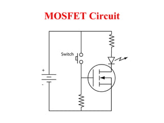
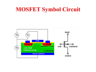
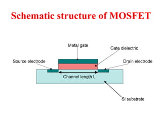
Metal Oxide Semiconductor Field Effect Transistor M.S.P.V.L Polytechnic College, Pavoorchatram.
MOSFET Circuit
MOSFET Symbol Circuit
Introduction A MOSFET ( Metal Oxide Semiconductor Field Effect Transistor ) is a semiconductor device.  A MOSFET is most commonly used in the field of power electronics.  A semiconductor is made of manufactured material that acts neither like a  insulator  nor a conductor. 
Structure of MOSFET
Schematic structure of MOSFET
Working principle of MOSFET A metal–oxide–semiconductor field-effect transistor (MOSFET) is based on the  modulation of charge concentration  by a MOS capacitance between a  body  electrode and a  gate  electrode located above the body and insulated from all other device regions by a gate dielectric layer which in the case of a MOSFET is an oxide, such as  silicon dioxide .
Working principle of MOSFET If dielectrics other than an oxide such as silicon dioxide (often referred to as oxide) are employed the device may be referred to as a metal–insulator–semiconductor FET (MISFET).  Compared to the MOS capacitor, the MOSFET includes two additional terminals ( source  and  drain ), each connected to individual highly doped regions that are separated by the body region. 
N and P channel of MOSFET
N and P channel of MOSFET If the MOSFET is an  n-channel  or  nMOS FET , then the source and drain are 'n+' regions and the body is a  'p'  region. If the MOSFET is a  p-channel  or  pMOS FET , then the source and drain are 'p+' regions and the body is a  'n'  region. 
Cross section of NMOS with channel- OFF state
Cross section of NMOS without channel- OFF state
When a  negative gate-source voltage  (positive source-gate) is applied, it creates a  p-channel  at the surface of the  n region , analogous to the n-channel case, but with opposite polarities of charges and voltages. When a  voltage less negative  than the threshold value (a negative voltage for p-channel) is applied between gate and source, the channel disappears and only a very small sub threshold current can flow between the  source and the drain . Working principle of MOSFET
Working principle of MOSFET
The device may comprise a  Silicon On Insulator  (SOI) device in which a  Buried Oxide  (BOX) is formed below a thin semiconductor layer.  If the channel region between the  gate dielectric  and a  Buried Oxide (BOX) region  is very thin, the very thin channel region is referred to as an  Ultra Thin Channel (UTC) region  with the source and drain regions formed on either side thereof in and/or above the thin semiconductor layer. Working principle of MOSFET
Alternatively, the device may comprise a  Semiconductor On Insulator (SEMOI)  device in which semiconductors other than silicon are employed.  When the source and drain regions are formed above the channel in whole or in part, they are referred to as  Raised Source/Drain (RSD) regions Working principle of MOSFET
The End ……  Thank You ……

Mosfet

  • 1.
    Metal Oxide Semiconductor Field Effect TransistorM.S.P.V.L Polytechnic College, Pavoorchatram.
  • 2.
  • 3.
  • 4.
    Introduction A MOSFET( Metal Oxide Semiconductor Field Effect Transistor ) is a semiconductor device. A MOSFET is most commonly used in the field of power electronics. A semiconductor is made of manufactured material that acts neither like a  insulator  nor a conductor. 
  • 5.
  • 6.
  • 7.
    Working principle ofMOSFET A metal–oxide–semiconductor field-effect transistor (MOSFET) is based on the modulation of charge concentration by a MOS capacitance between a  body  electrode and a  gate  electrode located above the body and insulated from all other device regions by a gate dielectric layer which in the case of a MOSFET is an oxide, such as silicon dioxide .
  • 8.
    Working principle ofMOSFET If dielectrics other than an oxide such as silicon dioxide (often referred to as oxide) are employed the device may be referred to as a metal–insulator–semiconductor FET (MISFET). Compared to the MOS capacitor, the MOSFET includes two additional terminals ( source  and  drain ), each connected to individual highly doped regions that are separated by the body region. 
  • 9.
    N and Pchannel of MOSFET
  • 10.
    N and Pchannel of MOSFET If the MOSFET is an n-channel or nMOS FET , then the source and drain are 'n+' regions and the body is a 'p' region. If the MOSFET is a p-channel or pMOS FET , then the source and drain are 'p+' regions and the body is a 'n' region. 
  • 11.
    Cross section ofNMOS with channel- OFF state
  • 12.
    Cross section ofNMOS without channel- OFF state
  • 13.
    When a negative gate-source voltage (positive source-gate) is applied, it creates a  p-channel  at the surface of the n region , analogous to the n-channel case, but with opposite polarities of charges and voltages. When a voltage less negative than the threshold value (a negative voltage for p-channel) is applied between gate and source, the channel disappears and only a very small sub threshold current can flow between the source and the drain . Working principle of MOSFET
  • 14.
  • 15.
    The device maycomprise a Silicon On Insulator (SOI) device in which a Buried Oxide (BOX) is formed below a thin semiconductor layer. If the channel region between the gate dielectric and a Buried Oxide (BOX) region is very thin, the very thin channel region is referred to as an Ultra Thin Channel (UTC) region with the source and drain regions formed on either side thereof in and/or above the thin semiconductor layer. Working principle of MOSFET
  • 16.
    Alternatively, the devicemay comprise a Semiconductor On Insulator (SEMOI) device in which semiconductors other than silicon are employed. When the source and drain regions are formed above the channel in whole or in part, they are referred to as Raised Source/Drain (RSD) regions Working principle of MOSFET
  • 17.
    The End …… Thank You ……