Downloaded 1,345 times


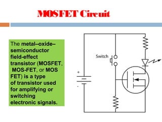
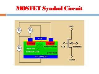
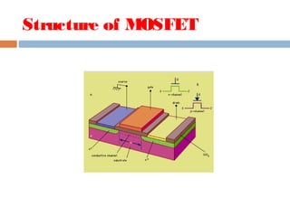
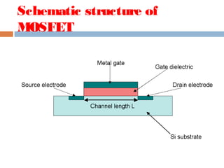
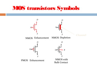
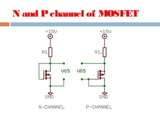


A MOSFET is a semiconductor device that can amplify or switch electronic signals. It has three terminals - drain, source, and gate. Depending on whether the semiconductor material between the drain and source is n-type or p-type, a MOSFET can be an n-channel or p-channel type. Applying a positive voltage to the gate of an n-channel MOSFET or a negative voltage to the gate of a p-channel MOSFET allows current to flow between the drain and source. MOSFETs are commonly used as switches in digital circuits like processors and as amplifiers in analog circuits. They are also used in memory devices, power supplies, and other electronic applications.