The document discusses different types of field effect transistors including JFETs and MOSFETs. It describes:
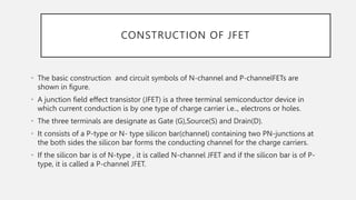
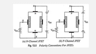
1. JFETs are classified as N-channel or P-channel depending on whether the conducting channel is made of N-type or P-type silicon. The gate controls the flow of current through the channel.
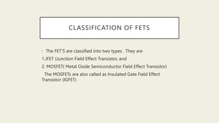
2. MOSFETs are categorized as depletion or enhancement type. Depletion MOSFETs can operate in depletion or enhancement mode while enhancement MOSFETs only operate in enhancement mode.
3. CMOSFETs use complementary pairs of enhancement-mode NMOS and PMOS transistors to function as inverters with very low power consumption.


![MUTUAL CHARACTERISTICS OF JFET
DEFINITION: The graph which show the relationship between the drain current (ID) and
the gate to source voltage (VGS) for constant value of drain to source voltage is called
“Mutual or transfer characteristics of JFET.”
ID=IDSS[1-VGS/ VGS(off)] 2
PARAMETERS OF JFET:
• A JFET has certain parameters which determine is performance in a circuit.
• The main parameters of JFET when connected in common source mode are :
1. A. C. DRAIN RESISTANCE(rd)
2. Trans-conductor(gm)
3. Amplification factor](https://image.slidesharecdn.com/akhilbee-231117155711-a503411e/85/FET-pptx-16-320.jpg)


![Aim-to study characterstics of fet (field effect [Autosaved].pptx](https://cdn.slidesharecdn.com/ss_thumbnails/aim-tostudycharactersticsoffetfieldeffectautosaved-221113041420-4dcee974-thumbnail.jpg?width=640&height=640&fit=bounds)


