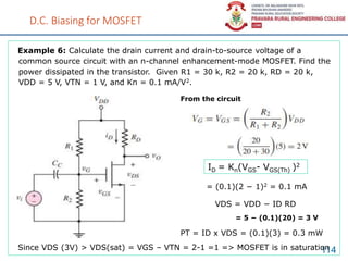
Download as PDF, PPTX


![UNIT-1 [MOSFET & its Analysis]
11](https://image.slidesharecdn.com/mosfetsmgcomplete-200823141903/85/MOSFET-complete-PPT-11-320.jpg)
![UNIT-1 [MOSFET & its Analysis]
Text Books:
• T1: Donald Neaman, “Electronic Circuits – Analysis and Design” Third edition, Mc
Graw Hill.
• T2: Ramakant Gaikwad, “Op amps & Linear Integrated Circuits”, PHI 4th Education.
• T3: Boylestad and Nashelsky “Electronic Devices and Circuit Theory” Prentice Hall
Seventh Edition
Reference Books:
• R1: Millman Halkias, “Integrated Electronics”.
• R2: Phillip E. Allen, Douglas R. Holberg, “CMOS Analog Circuit Design”, Second Edition,
Oxford.
• R3: Salivahan and Kanchana Bhaskaran, “Linear Integrated Circuits”, Tata McGraw
Hill.
• R4: Pucknell and Kamran
MOOC / NPTEL Courses:
1. NPTEL Course “Analog Electronic Circuits”
• https://nptel.ac.in/courses/108/105/108105158/
2. NPTEL Course on “Analog Circuits”
• https://nptel.ac.in/courses/108/101/108101094/
12](https://image.slidesharecdn.com/mosfetsmgcomplete-200823141903/85/MOSFET-complete-PPT-12-320.jpg)
![UNIT-2 [ MOSFET Circuits]
14](https://image.slidesharecdn.com/mosfetsmgcomplete-200823141903/85/MOSFET-complete-PPT-14-320.jpg)
![UNIT-2 [ MOSFET Circuits]
15](https://image.slidesharecdn.com/mosfetsmgcomplete-200823141903/85/MOSFET-complete-PPT-15-320.jpg)
![UNIT-2 [ MOSFET Circuits]
Text Books:
• T1: Donald Neaman, “Electronic Circuits – Analysis and Design” Third edition, Mc
Graw Hill.
• T2: Ramakant Gaikwad, “Op amps & Linear Integrated Circuits”, Pearson Education.
Reference Books:
• R1: Millman Halkias, “Integrated Electronics”.
• R2: Phillip E. Allen, Douglas R. Holberg, “CMOS Analog Circuit Design”, Second Edition,
Oxford.
• R3: Salivahan and Kanchana Bhaskaran, “Linear Integrated Circuits”, Tata McGraw
Hill.
MOOC / NPTEL Courses:
1. NPTEL Course “Analog Electronic Circuits”
• https://nptel.ac.in/courses/108/105/108105158/
2. NPTEL Course on “Analog Circuits”
• https://nptel.ac.in/courses/108/101/108101094/
16](https://image.slidesharecdn.com/mosfetsmgcomplete-200823141903/85/MOSFET-complete-PPT-16-320.jpg)

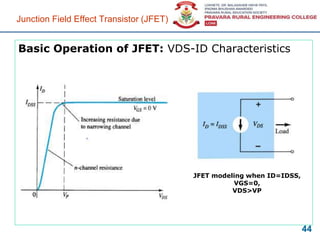
![UNIT-3 [Voltage Regulators]
18](https://image.slidesharecdn.com/mosfetsmgcomplete-200823141903/85/MOSFET-complete-PPT-18-320.jpg)
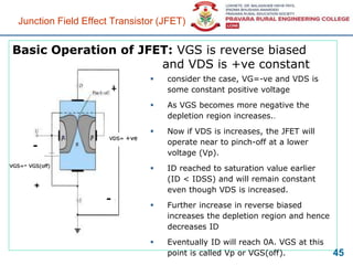
![UNIT-3 [Voltage Regulators]
Text Books:
• T1: Donald Neaman, “Electronic Circuits – Analysis and Design” Third edition, Mc
Graw Hill.
• T2: Ramakant Gaikwad, “Op amps & Linear Integrated Circuits”, Pearson Education.
• T3: K. R. Botkar, “Integrated Circuits” Page No: 27 to 772
Reference Books:
• R1: Millman Halkias, “Integrated Electronics”.
• R2: Phillip E. Allen, Douglas R. Holberg, “CMOS Analog Circuit Design”, Second Edition,
Oxford.
• R3: Salivahan and Kanchana Bhaskaran, “Linear Integrated Circuits”, Tata McGraw
Hill.
MOOC / NPTEL Courses:
1. NPTEL Course “Analog Electronic Circuits”
• https://nptel.ac.in/courses/108/105/108105158/
2. NPTEL Course on “Analog Circuits”
• https://nptel.ac.in/courses/108/101/108101094/
19](https://image.slidesharecdn.com/mosfetsmgcomplete-200823141903/85/MOSFET-complete-PPT-19-320.jpg)

![UNIT-4 [Operational Amplifier]
21](https://image.slidesharecdn.com/mosfetsmgcomplete-200823141903/85/MOSFET-complete-PPT-21-320.jpg)
![UNIT-4 [Operational Amplifier]
22](https://image.slidesharecdn.com/mosfetsmgcomplete-200823141903/85/MOSFET-complete-PPT-22-320.jpg)
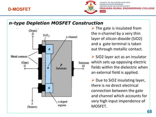
![UNIT-4 [Operational Amplifier]
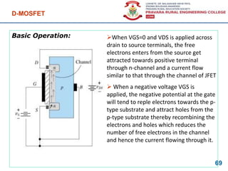
Text Books:
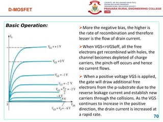
• T1: Donald Neaman, “Electronic Circuits – Analysis and Design” Third edition, Mc
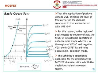
Graw Hill.
• T2: Ramakant Gaikwad, “Op amps & Linear Integrated Circuits”, PHI 4th Edition.
Reference Books:
• R1: Millman Halkias, “Integrated Electronics”.
• R2: Phillip E. Allen, Douglas R. Holberg, “CMOS Analog Circuit Design”, Second Edition,
Oxford.
• R3: Salivahan and Kanchana Bhaskaran, “Linear Integrated Circuits”, Tata McGraw
Hill.
MOOC / NPTEL Courses:
1. NPTEL Course “Analog Electronic Circuits”
• https://nptel.ac.in/courses/108/105/108105158/
2. NPTEL Course on “Analog Circuits”
• https://nptel.ac.in/courses/108/101/108101094/ 23](https://image.slidesharecdn.com/mosfetsmgcomplete-200823141903/85/MOSFET-complete-PPT-23-320.jpg)
![UNIT-5 [Op-Amp Applications]
25](https://image.slidesharecdn.com/mosfetsmgcomplete-200823141903/85/MOSFET-complete-PPT-25-320.jpg)
![UNIT-5 [Op-Amp Applications]
26](https://image.slidesharecdn.com/mosfetsmgcomplete-200823141903/85/MOSFET-complete-PPT-26-320.jpg)
![UNIT-5 [Op-Amp Applications]
27](https://image.slidesharecdn.com/mosfetsmgcomplete-200823141903/85/MOSFET-complete-PPT-27-320.jpg)
![UNIT-5 [Op-Amp Applications]
Text Books:
• T1: Donald Neaman, “Electronic Circuits – Analysis and Design” Third edition, Mc
Graw Hill.
• T2: Ramakant Gaikwad, “Op amps & Linear Integrated Circuits”, PHI 4th Education.
Reference Books:
• R1: Millman Halkias, “Integrated Electronics”.
• R2: Phillip E. Allen, Douglas R. Holberg, “CMOS Analog Circuit Design”, Second Edition,
Oxford.
• R3: Salivahan and Kanchana Bhaskaran, “Linear Integrated Circuits”, Tata McGraw
Hill.
MOOC / NPTEL Courses:
1. NPTEL Course “Analog Electronic Circuits”
• https://nptel.ac.in/courses/108/105/108105158/
2. NPTEL Course on “Analog Circuits”
• https://nptel.ac.in/courses/108/101/108101094/ 28](https://image.slidesharecdn.com/mosfetsmgcomplete-200823141903/85/MOSFET-complete-PPT-28-320.jpg)
![UNIT-6 [Converters & PLL]
30](https://image.slidesharecdn.com/mosfetsmgcomplete-200823141903/85/MOSFET-complete-PPT-30-320.jpg)
![UNIT-6 [Converters & PLL] ]
31](https://image.slidesharecdn.com/mosfetsmgcomplete-200823141903/85/MOSFET-complete-PPT-31-320.jpg)
![UNIT-6 [Converters & PLL]
Text Books:
• T1: Donald Neaman, “Electronic Circuits – Analysis and Design” Third edition, Mc
Graw Hill.
• T2: Ramakant Gaikwad, “Op amps & Linear Integrated Circuits”, Pearson Education.
Reference Books:
• R1: Millman Halkias, “Integrated Electronics”.
• R2: Phillip E. Allen, Douglas R. Holberg, “CMOS Analog Circuit Design”, Second Edition,
Oxford.
• R3: Salivahan and Kanchana Bhaskaran, “Linear Integrated Circuits”, Tata McGraw
Hill.
MOOC / NPTEL Courses:
1. NPTEL Course “Analog Electronic Circuits”
• https://nptel.ac.in/courses/108/105/108105158/
2. NPTEL Course on “Analog Circuits”
• https://nptel.ac.in/courses/108/101/108101094/ 32](https://image.slidesharecdn.com/mosfetsmgcomplete-200823141903/85/MOSFET-complete-PPT-32-320.jpg)


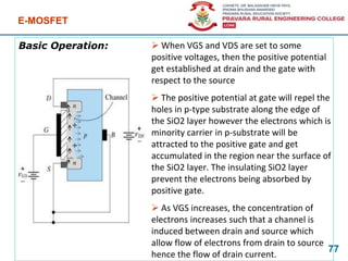
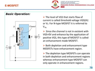
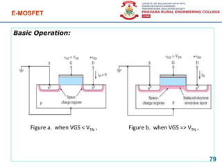
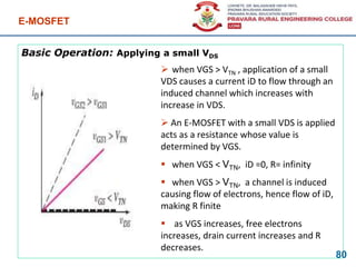
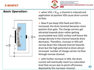

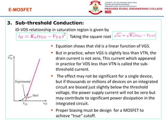
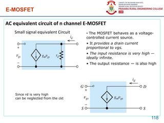
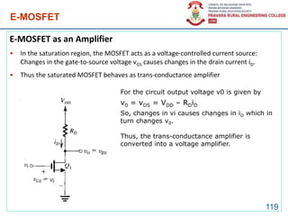
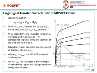
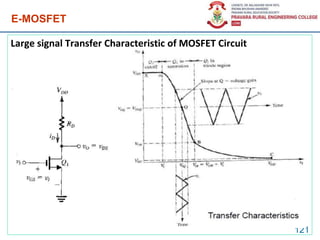
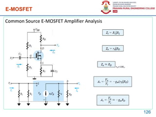
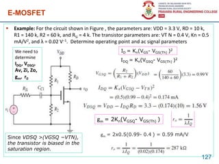
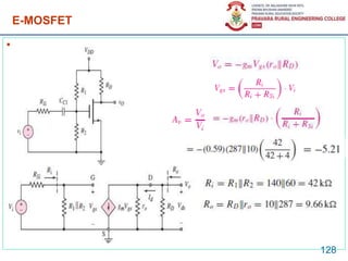
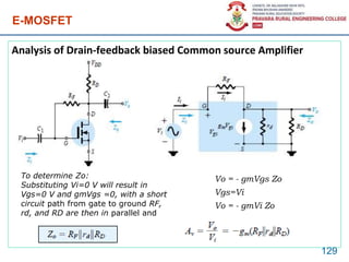
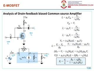
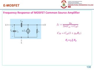
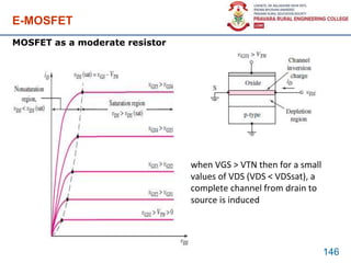

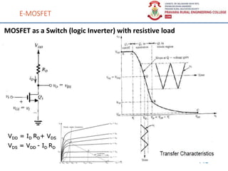
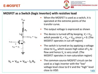
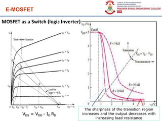
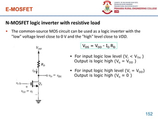
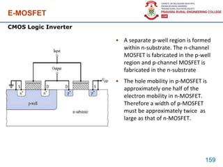
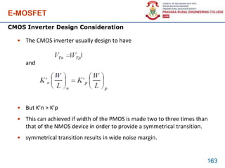
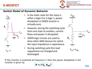
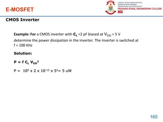
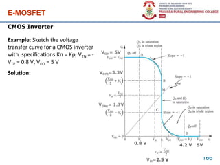
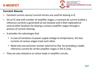
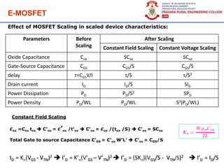
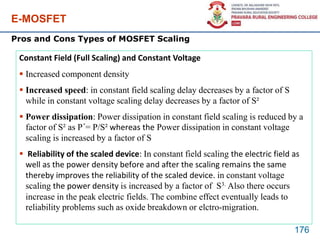
![E-MOSFET
MOSFET as a Switch (logic Inverter) with resistive load
150
• In non-saturation region, iD is given by
iD = Kn[2(vGS-VTN )vDS –vDS
2]
iD = Kn[2(vi-VTN )v0–v0
2]
v0 = VDS = VDD - ID RD
v0 = VDD - KnRD[2(vi-VTN )v0–v0
2]](https://image.slidesharecdn.com/mosfetsmgcomplete-200823141903/85/MOSFET-complete-PPT-150-320.jpg)
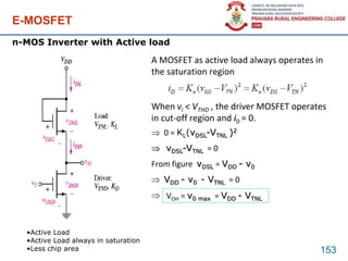
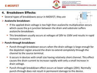
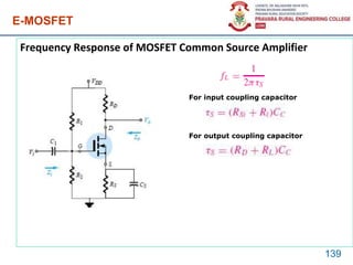
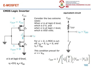
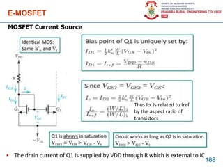
![E-MOSFET
154
n-MOS Inverter with Active load
When vi = VDD, driver MOSFET operates in non-saturation
region
iDD = KD[2(vGSD-VTND )vDSD –vDSD
2]
iDD = KD[2(vi-VTND )v0–v0
2]
Since iDD = iDL = KL(vDSL-VTNL )2
KD[2(vi-VTND )v0–v0
2] = KL(VDD - v0 -VTNL )2
Which indicate that the relation between vi and vo is
nonlinear.
KD/KL=(W/L)D /(W/L)L
The conduction parameter can be expressed in terms
of aspect ratio of MOSFET as
KD=(k’D/2 )(W/L)D similarly KL=(k’L/2 )(W/L)L
The above equations can be used in design of NMOS
inverter](https://image.slidesharecdn.com/mosfetsmgcomplete-200823141903/85/MOSFET-complete-PPT-154-320.jpg)
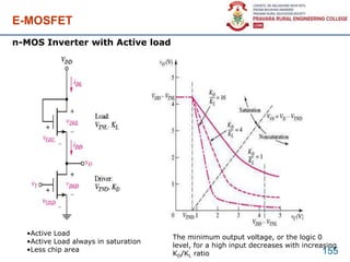
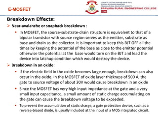
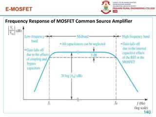
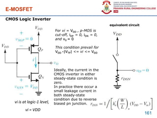
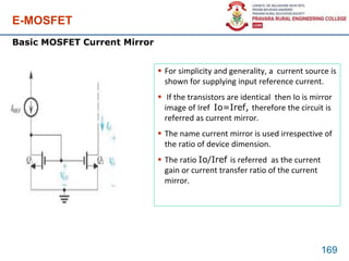
![E-MOSFET
156
n-MOS Inverter with Active load
Example: Design a NMOS inverter for v0 =0.10 V and vi =2.5 V
Given VDD = 3V, k’n = 60uA/V2 ,VTN = 0.5V
Also determine the power dissipation in the inverter
Solution: Since iDD (non-saturation) = iDL(saturation)
KD[2(vGSD-VTND )vDSD–vDSD
2] = KL(vGSL -VTNL )2
vGSD=vi vDSD=v0 and vGSL=vDSL=VDD - v0
KD[2(vi-VTND )v0–v0
2] = KL(VDD - v0 -VTNL )2
KD[2(2.5 - 0.5)(0.1)– (0.1)2] = KL(3 – 0.1 – 0.5)2
KD/KL= 14.8 = (W/L)D /(W/L)L
Assuming (W/L)L = 1 => (W/L)D = 14.8
iD = iDD = iDL =KL(VDD - v0 -VTNL )2
KL=k’L/2 (W/L)L = 60/2 (1) =30 uA/V2
iD = 30(3 – 0.1 – 0.5 )2 = 172.8 uA
P = iDVDD = 172.8 x 3 = 518.4 uW
High power dissipation](https://image.slidesharecdn.com/mosfetsmgcomplete-200823141903/85/MOSFET-complete-PPT-156-320.jpg)
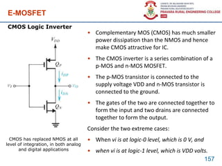
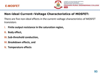
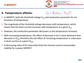
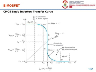
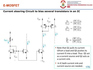
![E-MOSFET
158
CMOS Logic Inverter n-MOSFET p-MOSFET
Cut-off region vGS < VTN vSG < |VTP|
Saturation region
vDS > vDS(sat)
iD = Kn(vGS - VTN)2 iD = Kp(vSG + VTP )2
vDS(sat) = (vGS - VTN) vDS(sat) = (vSG + VTP)
Non saturation region
vDS < vDS(sat)
iD= Kn[2(vGS-VTN )vDS –vDS
2] iD= Kp[2(vSG + VTP )vSD –vSD
2]
Parameters Kn, VTN and VTN > 0 Kp, VTP and VTP < 0](https://image.slidesharecdn.com/mosfetsmgcomplete-200823141903/85/MOSFET-complete-PPT-158-320.jpg)
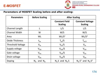

The document outlines a comprehensive syllabus for a second-year electronics engineering course focused on electronic circuits, primarily discussing MOSFETs, operational amplifiers, voltage regulators, and data conversion techniques. Key learning objectives include understanding semiconductor device characteristics, designing amplifiers and oscillators, and analyzing linear and switching regulators. Various course outcomes emphasize students' abilities to apply theoretical concepts in practical scenarios, supported by recommended textbooks and online courses for further learning.