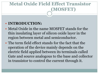
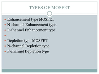
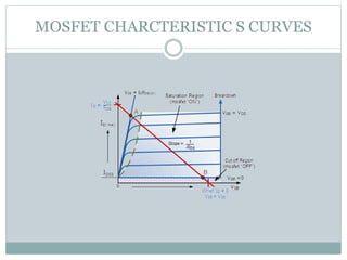
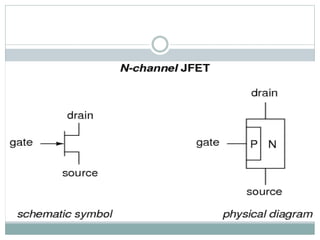
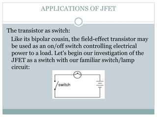
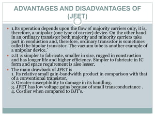
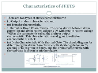
FETS(MOSFET AND JFETS)
BASIC ELECRONIS
BY:SYED SUMAIR HASSAN (k14-2850)
Metal Oxide Field Effect Transistor
(MOSFET)
 INTRODUCTION:
 Metal Oxide in the name MOSFET stands for the
thin insulating layer of silicon oxide layer in the
region between metal and semiconductor.
 The term field effect stands for the fact that the
operation of the device mainly depends on the
electric field applied between its terminals called
Gate and source analogous to the base and collector
in transistor to control the current through it.
TYPES OF MOSFET
 Enhancement type MOSFET
 N-channel Enhancement type
 P-channel Enhancement type

 Depletion type MOSFET
 N-channel Depletion type
 P-channel Depletion type
APPLICATIONS OF MOSFET
 The MOSFET as a Switch
 We saw previously, that the N-channel,
Enhancement-mode MOSFET (e-MOSFET)
operates using a positive input voltage and has
an extremely high input resistance (almost
infinite) making it possible to interface with
nearly any logic gate or driver capable of
producing a positive output. Also, due to this
very high input (Gate) resistance we can parallel
together many different MOSFETs until we
achieve the current handling limit required.
MOSFET CHARCTERISTIC S CURVES
JFET(JUNCTION FIELD
EFFECT TRANSISTOR)
ITNRODUCTION:
A transistor is a linear semiconductor device that controls
current with the application of a lower-power electrical
signal. Transistors may be roughly grouped into two
major divisions: bipolar and field-effect. In the last
chapter we studied bipolar transistors, which utilize a
small current to control a large current. In this chapter,
we'll introduce the general concept of the field-effect
transistor -- a device utilizing a smallvoltage to control
current -- and then focus on one particular type:
the junction field-effect transistor. In the next chapter
we'll explore another type of field-effect transistor,
the insulated gate variety.
APPLICATIONS OF JFET
The transistor as switch:
Like its bipolar cousin, the field-effect transistor may
be used as an on/off switch controlling electrical
power to a load. Let's begin our investigation of the
JFET as a switch with our familiar switch/lamp
circuit:
ADVANTAGES AND DISADVANTAGES OF
(JFET)
 1.Its operation depends upon the flow of majority carriers only, it is,
therefore, a unipolar (one type of carrier) device. On the other hand
in an ordinary transistor both majority and minority carriers take
part in conduction and, therefore, ordinary transistor is sometimes
called the bipolar transistor. The vacuum tube is another example of
a unipolar device.’
 2.It is simpler to fabricate, smaller in size, rugged in construction
and has longer life and higher efficiency. Simpler to fabricate in IC
form and space requirement is also lesser.
 The main drawback of JFET is
1. Its relative small gain-bandwidth product in comparison with that
of a conventional transistor.
2. Greater susceptibility to damage in its handling.
3. JFET has low voltage gains because of small transconductance .
4. Costlier when compared to BJT’s.
Characteristics of JFETS
 There are two types of static characteristics viz
 (1) Output or drain characteristic and
 (2) Transfer characteristic.
 1. Output or Drain Characteristic. The curve drawn between drain
current Ip and drain-source voltage VDS with gate-to source voltage
VGS as the parameter is called the drain or output
characteristic. This characteristic is analogous to collector
characteristic of a BJT:
 (a) Drain Characteristic With Shorted-Gate. The circuit diagram for
determining the drain characteristic with shorted-gate for an N-
channel JFET is given in figure. and the drain characteristic with
shorted-gate is shown in another figure.

MOSFET AND JFET

MOSFET AND JFET

  • 1.
    FETS(MOSFET AND JFETS) BASICELECRONIS BY:SYED SUMAIR HASSAN (k14-2850)
  • 2.
    Metal Oxide FieldEffect Transistor (MOSFET)  INTRODUCTION:  Metal Oxide in the name MOSFET stands for the thin insulating layer of silicon oxide layer in the region between metal and semiconductor.  The term field effect stands for the fact that the operation of the device mainly depends on the electric field applied between its terminals called Gate and source analogous to the base and collector in transistor to control the current through it.
  • 3.
    TYPES OF MOSFET Enhancement type MOSFET  N-channel Enhancement type  P-channel Enhancement type   Depletion type MOSFET  N-channel Depletion type  P-channel Depletion type
  • 4.
    APPLICATIONS OF MOSFET The MOSFET as a Switch  We saw previously, that the N-channel, Enhancement-mode MOSFET (e-MOSFET) operates using a positive input voltage and has an extremely high input resistance (almost infinite) making it possible to interface with nearly any logic gate or driver capable of producing a positive output. Also, due to this very high input (Gate) resistance we can parallel together many different MOSFETs until we achieve the current handling limit required.
  • 5.
  • 6.
    JFET(JUNCTION FIELD EFFECT TRANSISTOR) ITNRODUCTION: Atransistor is a linear semiconductor device that controls current with the application of a lower-power electrical signal. Transistors may be roughly grouped into two major divisions: bipolar and field-effect. In the last chapter we studied bipolar transistors, which utilize a small current to control a large current. In this chapter, we'll introduce the general concept of the field-effect transistor -- a device utilizing a smallvoltage to control current -- and then focus on one particular type: the junction field-effect transistor. In the next chapter we'll explore another type of field-effect transistor, the insulated gate variety.
  • 8.
    APPLICATIONS OF JFET Thetransistor as switch: Like its bipolar cousin, the field-effect transistor may be used as an on/off switch controlling electrical power to a load. Let's begin our investigation of the JFET as a switch with our familiar switch/lamp circuit:
  • 9.
    ADVANTAGES AND DISADVANTAGESOF (JFET)  1.Its operation depends upon the flow of majority carriers only, it is, therefore, a unipolar (one type of carrier) device. On the other hand in an ordinary transistor both majority and minority carriers take part in conduction and, therefore, ordinary transistor is sometimes called the bipolar transistor. The vacuum tube is another example of a unipolar device.’  2.It is simpler to fabricate, smaller in size, rugged in construction and has longer life and higher efficiency. Simpler to fabricate in IC form and space requirement is also lesser.  The main drawback of JFET is 1. Its relative small gain-bandwidth product in comparison with that of a conventional transistor. 2. Greater susceptibility to damage in its handling. 3. JFET has low voltage gains because of small transconductance . 4. Costlier when compared to BJT’s.
  • 10.
    Characteristics of JFETS There are two types of static characteristics viz  (1) Output or drain characteristic and  (2) Transfer characteristic.  1. Output or Drain Characteristic. The curve drawn between drain current Ip and drain-source voltage VDS with gate-to source voltage VGS as the parameter is called the drain or output characteristic. This characteristic is analogous to collector characteristic of a BJT:  (a) Drain Characteristic With Shorted-Gate. The circuit diagram for determining the drain characteristic with shorted-gate for an N- channel JFET is given in figure. and the drain characteristic with shorted-gate is shown in another figure. 