


![𝑽 𝑮𝑺 ≥ 𝟎
Voltage from gate to source is
controlling voltage of the JFET.
As 𝐕 𝐆𝐒 becomes more negative, the
depletion region increases.
The more negative 𝐕 𝐆𝐒, the resulting
level for 𝐈 𝐃 is reduced.
Eventually, when 𝐕 𝐆𝐒 = 𝐕𝐩 [Vp = VGS
(off)], ID is 0 mA. (the device is
“turned off”.](https://image.slidesharecdn.com/fetstransistor-181219065219/75/Field-Effect-Transistor-19-2048.jpg)
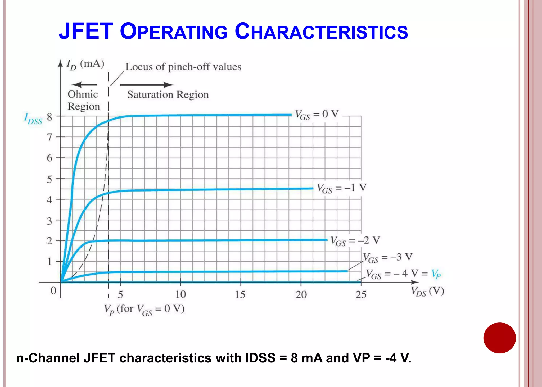
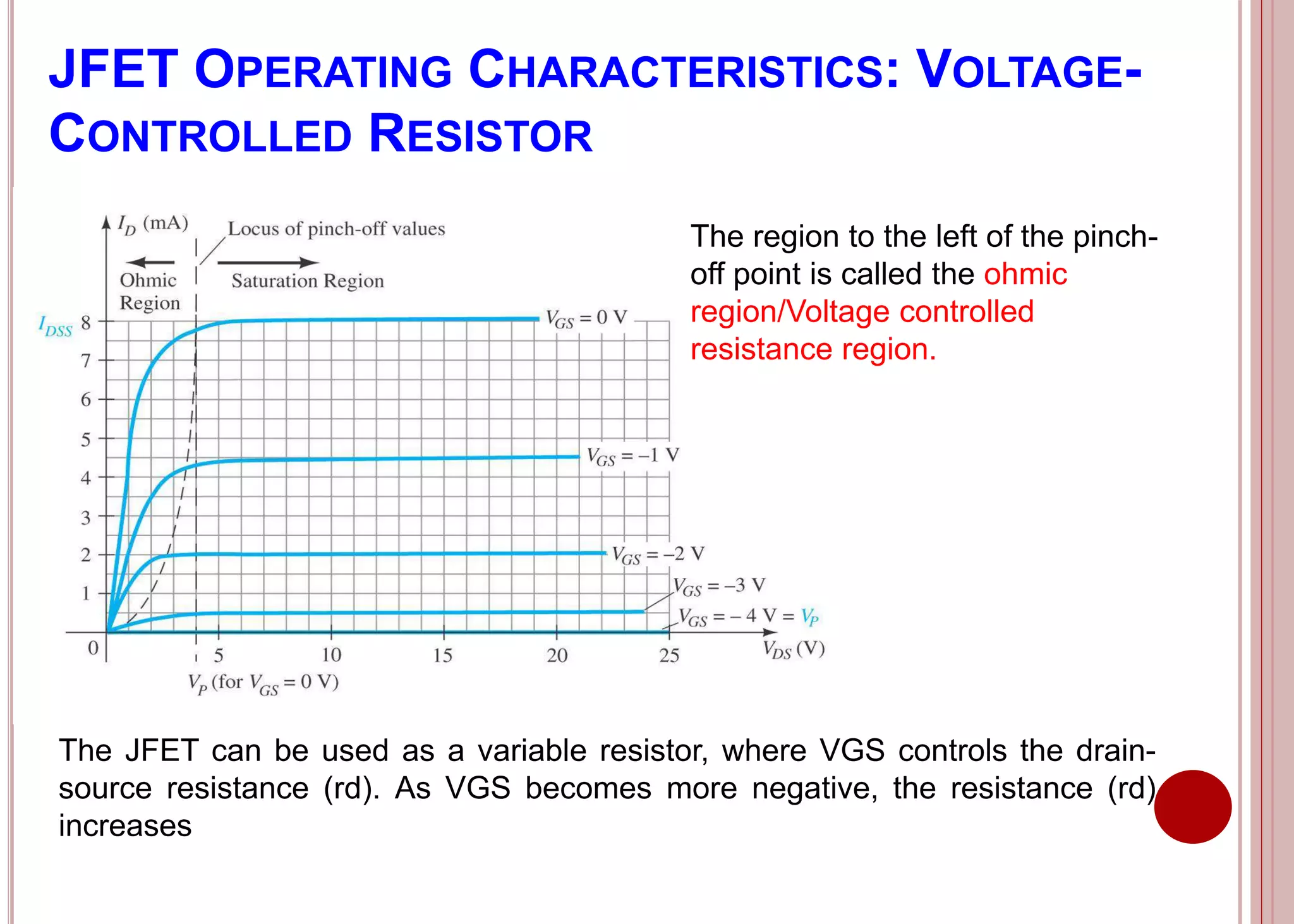
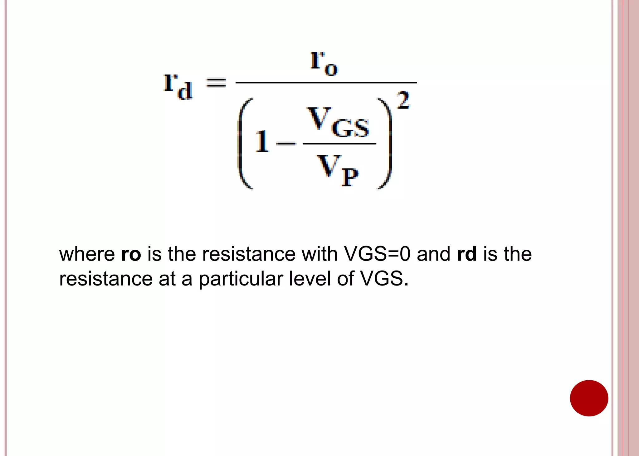


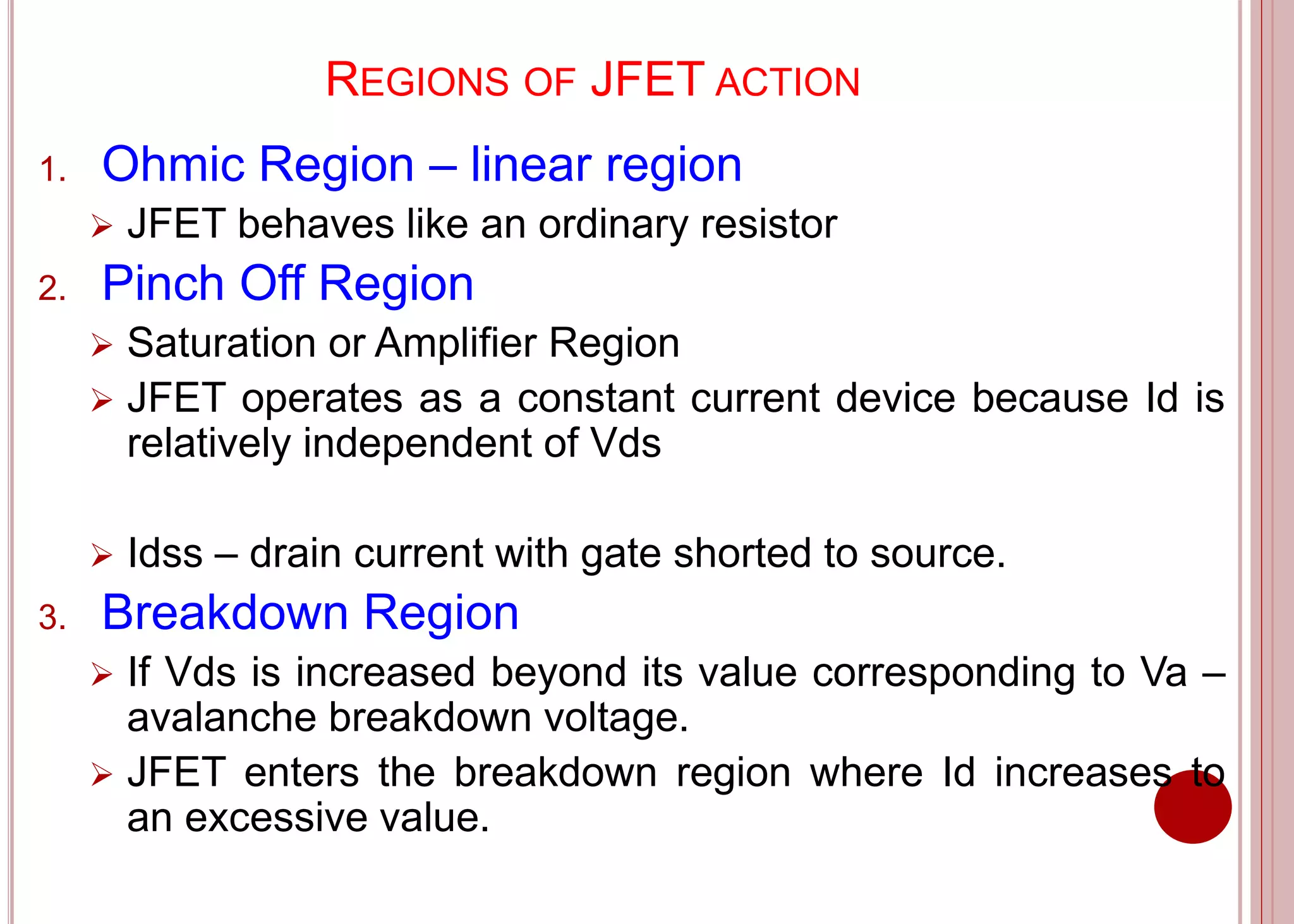
The document compares Field Effect Transistors (FETs) and Bipolar Junction Transistors (BJTs), highlighting their similarities and differences. It details various types of FETs, particularly Junction FETs (JFETs) and Metal-Oxide-Semiconductor FETs (MOSFETs), explaining their construction, operating characteristics, and transfer curves. Additionally, it briefly discusses important parameters and applications of these transistors in electronic circuits.


