Downloaded 135 times
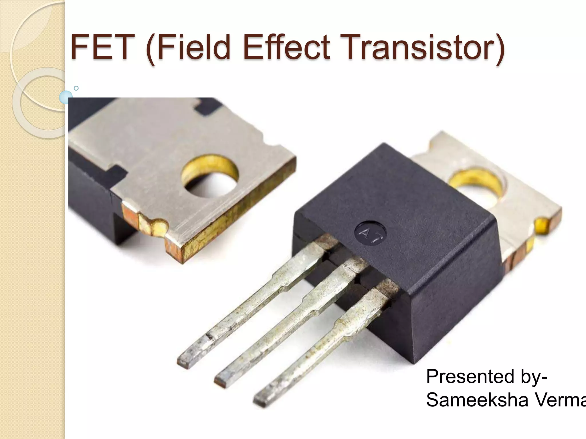
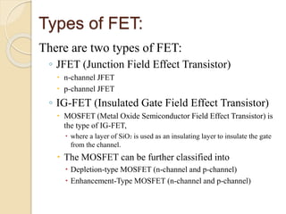
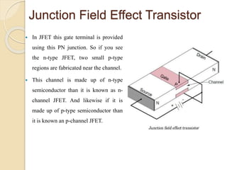


The document discusses Field Effect Transistors (FETs), focusing on their key components, types, and advantages over Bipolar Junction Transistors (BJTs), such as higher input impedance and lower noise levels. It details different FET types, including Junction Field Effect Transistors (JFETs) and Insulated Gate Field Effect Transistors (IG-FETs or MOSFETs), along with their operational characteristics and applications. FETs are highlighted as advantageous for their small size, efficiency, and high power gain, while also noting some disadvantages like lower voltage gain and higher costs compared to BJTs.


![Aim-to study characterstics of fet (field effect [Autosaved].pptx](https://cdn.slidesharecdn.com/ss_thumbnails/aim-tostudycharactersticsoffetfieldeffectautosaved-221113041420-4dcee974-thumbnail.jpg?width=640&height=640&fit=bounds)


