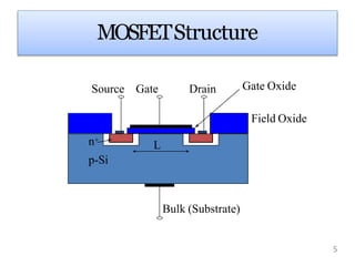
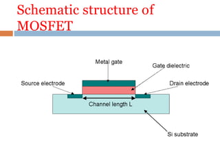
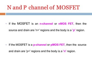
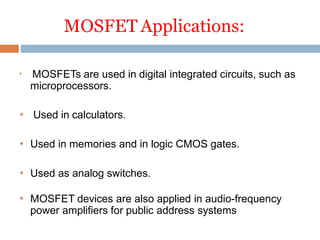
WELCOME TO MY
PRESENTATION
2
Sonargon university
Department of mechanical
Md.Touhid islam
Id:BME1703013073
Sec:whinchat
Metal OxideSemiconductor
FET(MOSFET)
3
MOSFET
 A MOSFET (Metal Oxide Semiconductor Field Effect Transistor)
is a semiconductor device.
 A MOSFET is most commonly used in the field of power electronics.
 A semiconductor is made of manufactured material that acts neither
like a insulator nor a conductor.
 Types
MOSFETStructure
n+
L
Source Gate Drain
Field Oxide
Gate Oxide
p-Si
Bulk (Substrate)
5
Schematic structure of
MOSFET
Working principle of MOSFET




Theworkingprincipleof MOSFET dependsuponthe
MOS capacitor.
TheMOS capacitoristhemainpart.
Thesemiconductorsurfaceatbelowtheoxidelayerand
betweenthedrainandsourceterminalcanbeinverted
fromp-typeton-typebyapplyingapositiveornegative
gatevoltagesrespectively.
When weapply positive gate voltage the holes present
beneath the oxide layer experience repulsive force and
theholesarepusheddownwardwiththesubstrate
Working principle of MOSFET
The depletion region is populated by the bound negative
charges, which are associated with the acceptor atoms.
The positive voltage also attracts electrons from the n+
source and drain regions in to the channel.
The electron reach channel is formed. Now, if a voltage is
applied between the source and the drain, current flows freely
between the source and drain gate voltage controls the
electrons concentration the channel.
Instead of positive if apply negative voltage a hole channel will
be formed beneath the oxide layer.
Basic Operation
Before After
10
MOS transistors Symbols
D
S
G
D
G
G
S
G
NMOS Enhancement
D
PMOS
S
NMOS Depletion
D
Enhancement
B
S
NMOS with
Bulk Contact
Channel
N and P channel of MOSFET
 If the MOSFET is an n-channel or nMOS FET, then the
source and drain are 'n+' regions and the body is a 'p' region.
 If the MOSFET is a p-channel or pMOS FET, then the source
and drain are 'p+' regions and the body is a 'n' region.
8
vGS > Vt ,small vDS
applied.
the channel
conductance
is proportional
to vGS - Vt,
and is
proportional
to (vGS - Vt)
vDSS.eptember 17, 2007
Triode
Region
September 17, 2007 9
vGS > Vt.
The induced
channel acquires
a tapered shape
and its
resistance
increases as vDS
is increased.
Saturation
Region
September 17, 2007 12
Enhancement-type NMOS transistor operated with vGS > Vt.
Drain current iD versus vDS
MOSFET Applications:

MOSFETs are used in digital integrated circuits, such as
microprocessors.
 Used in calculators.
 Used in memories and in logic CMOS gates.
 Used as analog switches.
 MOSFET devices are also applied in audio-frequency
power amplifiers for public address systems
MOSFET Applications
• Used as amplifiers.
• Used in the applications of power electronics and switch
mode power supplies.
• MOSFETs are used as oscillators in radio systems.
• Used in automobile sound systems and in sound
reinforcement systems
JEFTvsMOSFET
JEFT MOSFET
1. High input impedance 1. Very high input impedance
2. It canbe operated only indepletion
mode.
2. It canbe operated both depletionand
enhancement mode.
3. High gate current 3. Low gate current
4. High drain resistance 4. Low drain resistance
5. Conductivity is controlled bythe
reverse biasing of the gate
5. Conductivity is controlled bythe
carriers induced in the channel
6. Schematic symbol 6. Schematic symbol
7.Transconductance curve 7.Transconductance curve
30
Summary of
presentation
Mosfet detail
Mosfet detail

Mosfet detail

  • 1.
  • 2.
    2 Sonargon university Department ofmechanical Md.Touhid islam Id:BME1703013073 Sec:whinchat
  • 3.
  • 4.
    MOSFET  A MOSFET(Metal Oxide Semiconductor Field Effect Transistor) is a semiconductor device.  A MOSFET is most commonly used in the field of power electronics.  A semiconductor is made of manufactured material that acts neither like a insulator nor a conductor.  Types
  • 5.
    MOSFETStructure n+ L Source Gate Drain FieldOxide Gate Oxide p-Si Bulk (Substrate) 5
  • 6.
  • 7.
    Working principle ofMOSFET     Theworkingprincipleof MOSFET dependsuponthe MOS capacitor. TheMOS capacitoristhemainpart. Thesemiconductorsurfaceatbelowtheoxidelayerand betweenthedrainandsourceterminalcanbeinverted fromp-typeton-typebyapplyingapositiveornegative gatevoltagesrespectively. When weapply positive gate voltage the holes present beneath the oxide layer experience repulsive force and theholesarepusheddownwardwiththesubstrate
  • 8.
  • 9.
    Working principle ofMOSFET The depletion region is populated by the bound negative charges, which are associated with the acceptor atoms. The positive voltage also attracts electrons from the n+ source and drain regions in to the channel. The electron reach channel is formed. Now, if a voltage is applied between the source and the drain, current flows freely between the source and drain gate voltage controls the electrons concentration the channel. Instead of positive if apply negative voltage a hole channel will be formed beneath the oxide layer.
  • 10.
  • 11.
    MOS transistors Symbols D S G D G G S G NMOSEnhancement D PMOS S NMOS Depletion D Enhancement B S NMOS with Bulk Contact Channel
  • 12.
    N and Pchannel of MOSFET
  • 13.
    N and Pchannel of MOSFET  If the MOSFET is an n-channel or nMOS FET, then the source and drain are 'n+' regions and the body is a 'p' region.  If the MOSFET is a p-channel or pMOS FET, then the source and drain are 'p+' regions and the body is a 'n' region.
  • 14.
    8 vGS > Vt,small vDS applied. the channel conductance is proportional to vGS - Vt, and is proportional to (vGS - Vt) vDSS.eptember 17, 2007 Triode Region
  • 15.
    September 17, 20079 vGS > Vt. The induced channel acquires a tapered shape and its resistance increases as vDS is increased. Saturation Region
  • 16.
    September 17, 200712 Enhancement-type NMOS transistor operated with vGS > Vt. Drain current iD versus vDS
  • 17.
    MOSFET Applications:  MOSFETs areused in digital integrated circuits, such as microprocessors.  Used in calculators.  Used in memories and in logic CMOS gates.  Used as analog switches.  MOSFET devices are also applied in audio-frequency power amplifiers for public address systems
  • 18.
    MOSFET Applications • Usedas amplifiers. • Used in the applications of power electronics and switch mode power supplies. • MOSFETs are used as oscillators in radio systems. • Used in automobile sound systems and in sound reinforcement systems
  • 19.
    JEFTvsMOSFET JEFT MOSFET 1. Highinput impedance 1. Very high input impedance 2. It canbe operated only indepletion mode. 2. It canbe operated both depletionand enhancement mode. 3. High gate current 3. Low gate current 4. High drain resistance 4. Low drain resistance 5. Conductivity is controlled bythe reverse biasing of the gate 5. Conductivity is controlled bythe carriers induced in the channel 6. Schematic symbol 6. Schematic symbol 7.Transconductance curve 7.Transconductance curve 30
  • 20.

Editor's Notes