This document discusses field effect transistors (FETs) and provides details about junction FETs (JFETs). It describes the basic structure and operation of N-channel and P-channel JFETs. Key points covered include:
- FETs are voltage-controlled, unipolar devices that come in two main types: JFETs and MOSFETs.
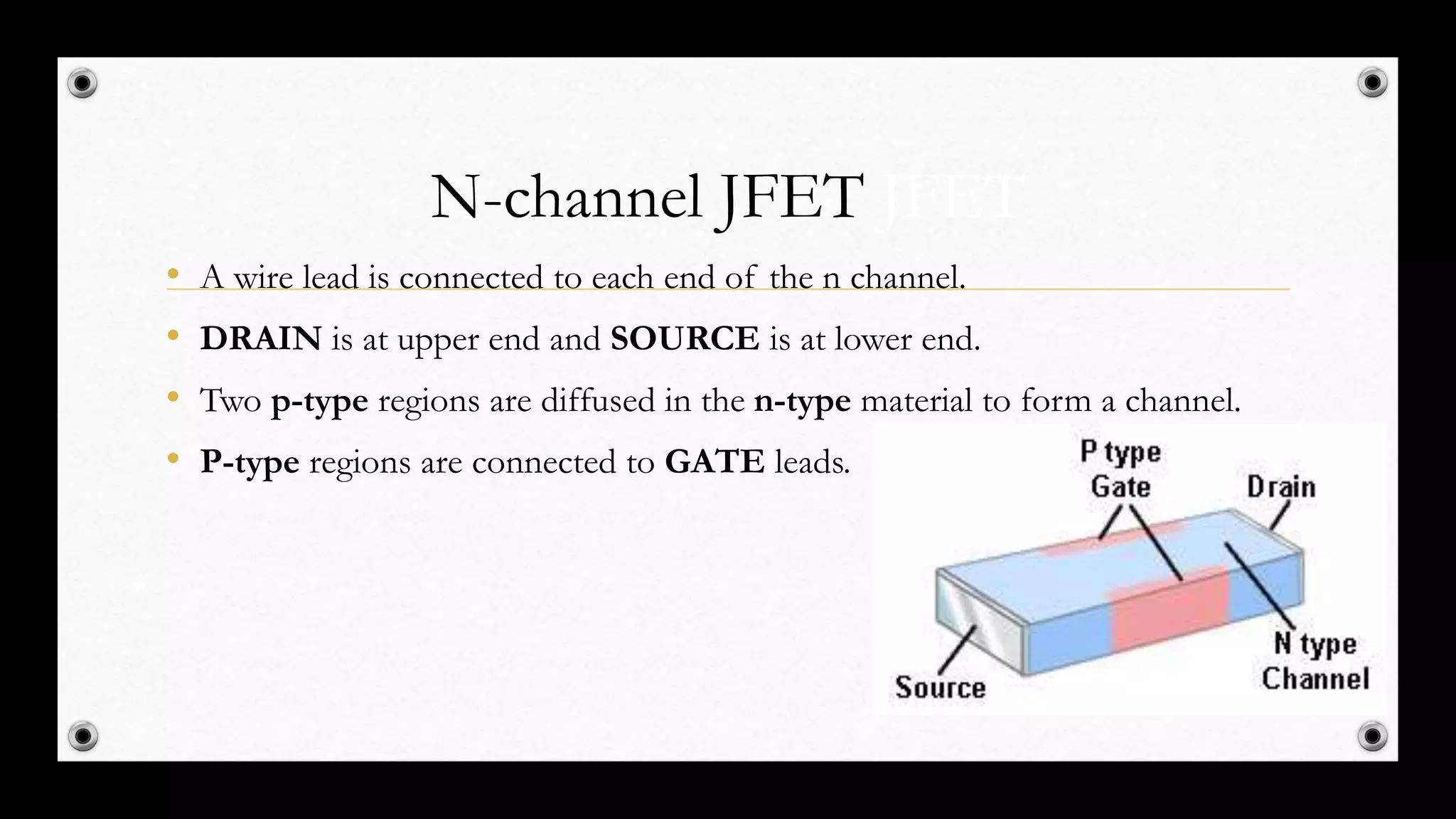
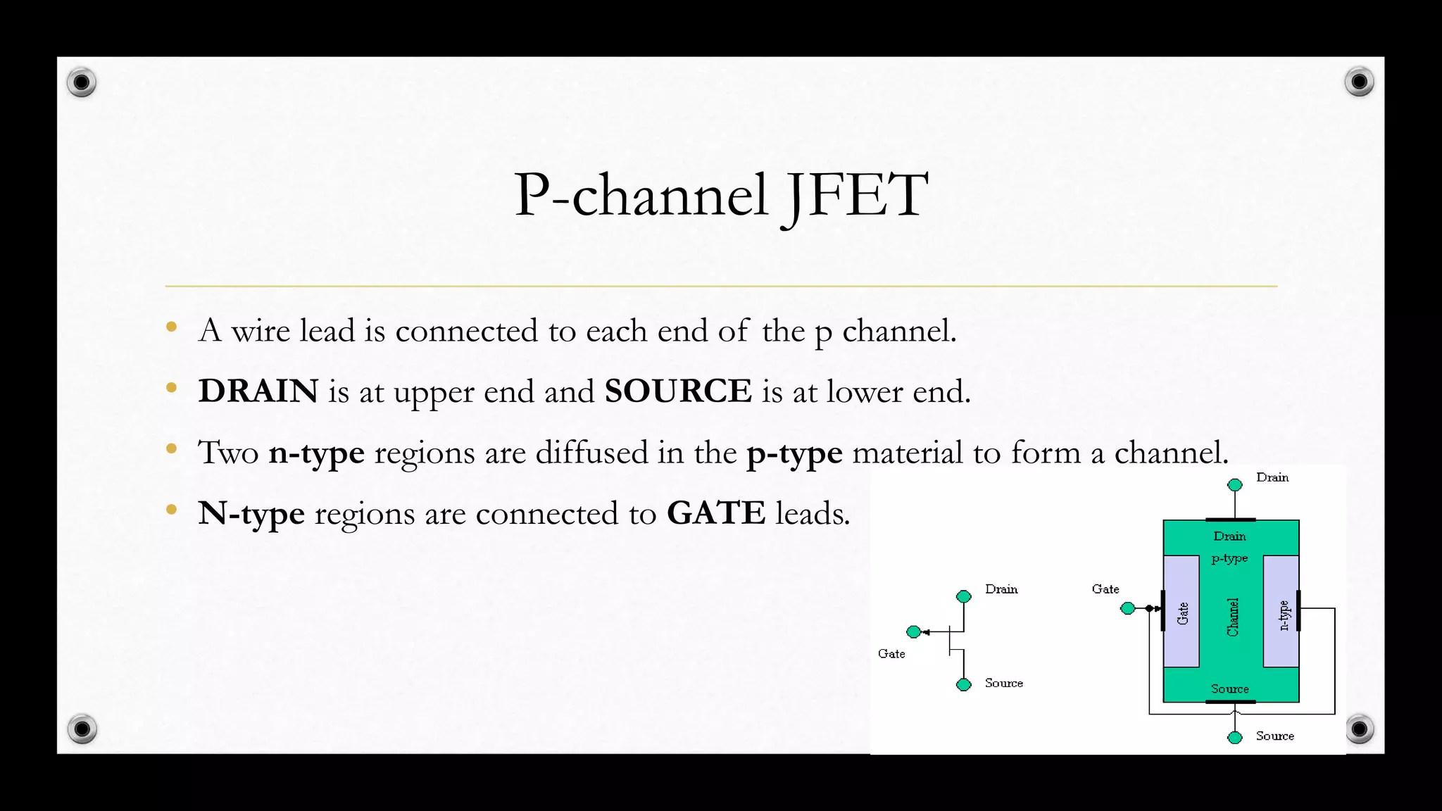
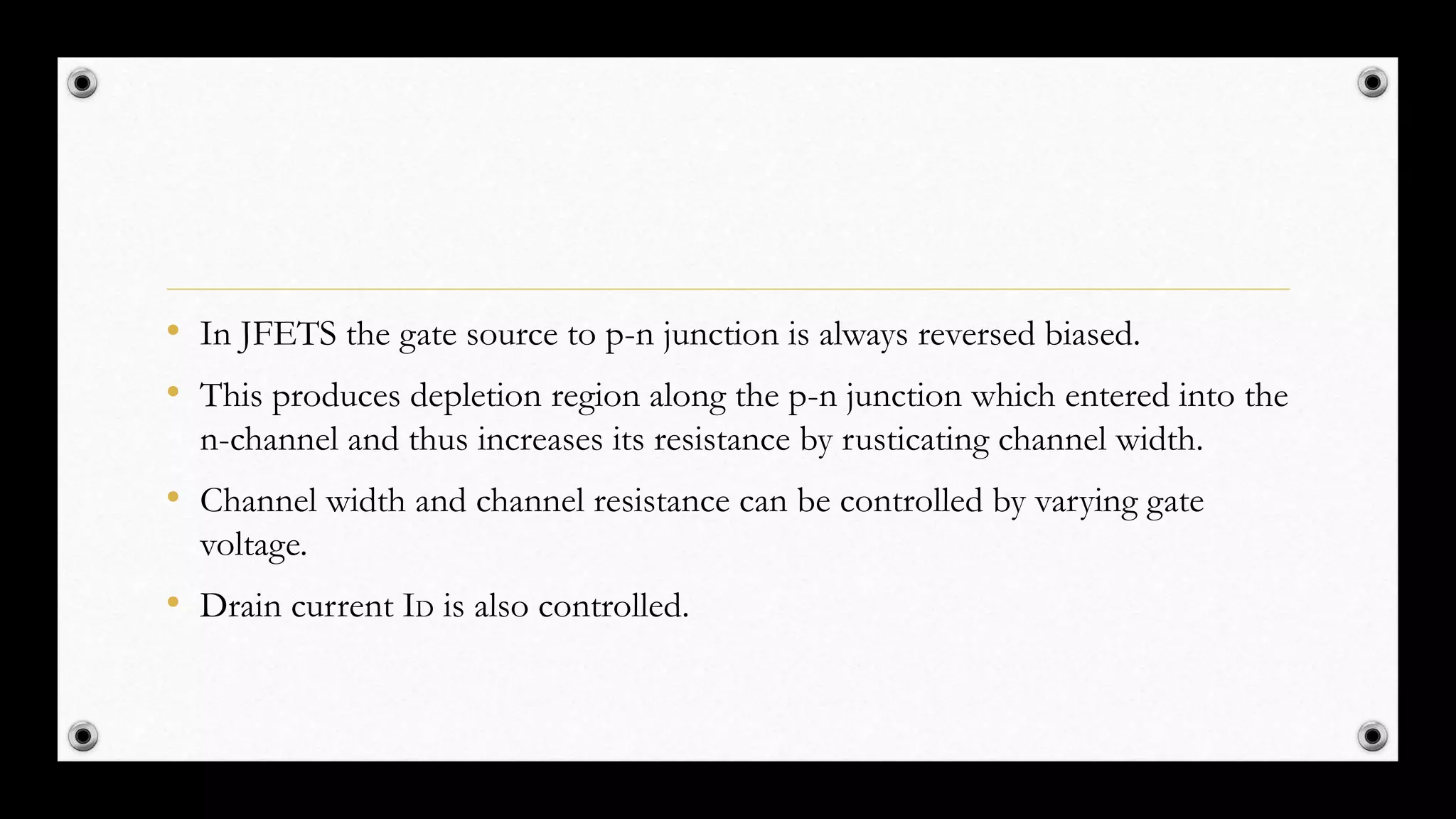
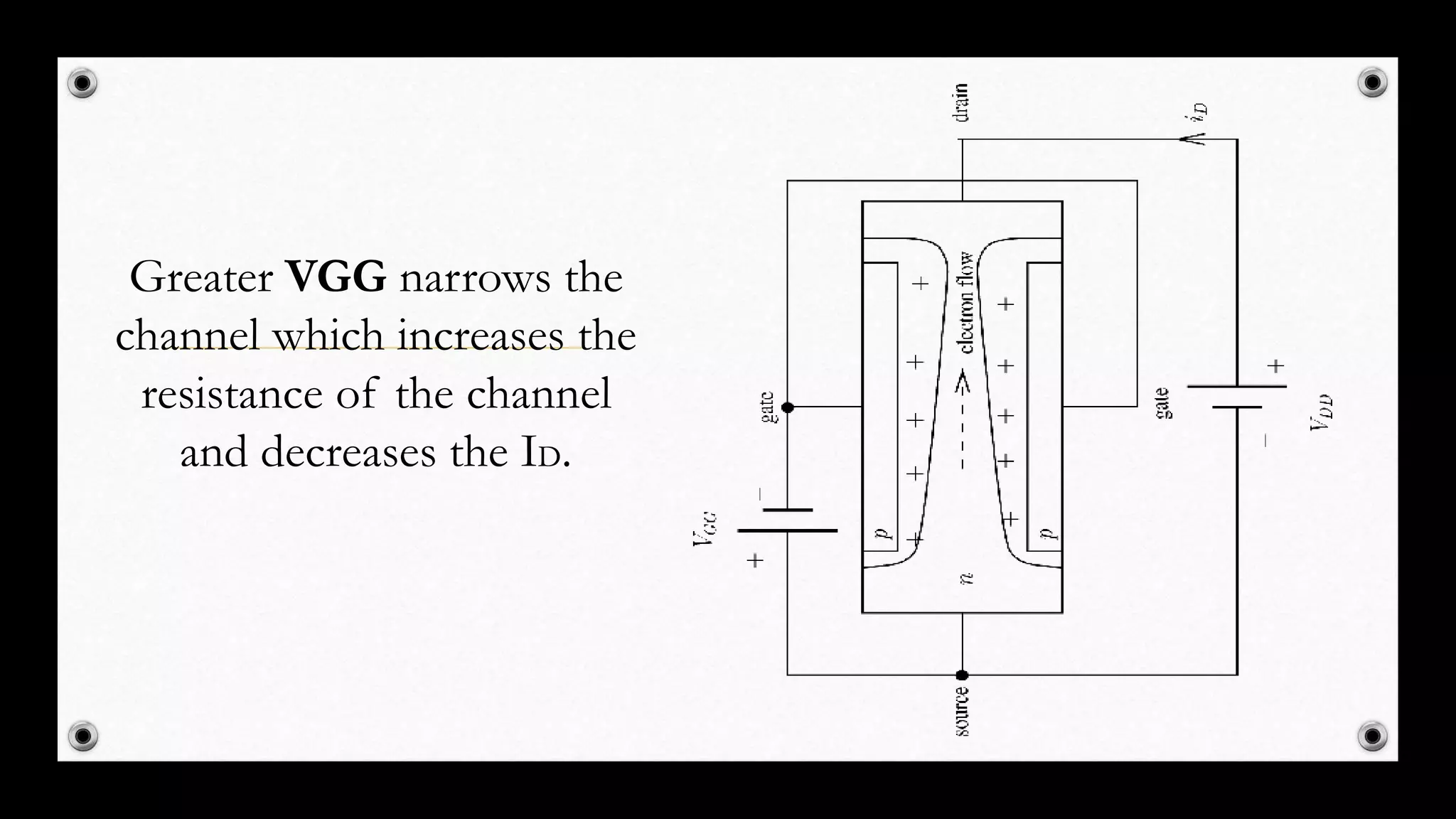
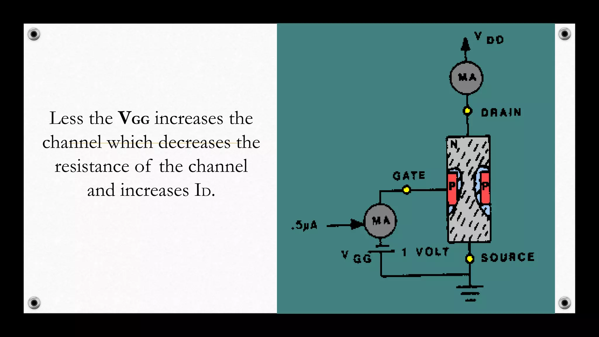
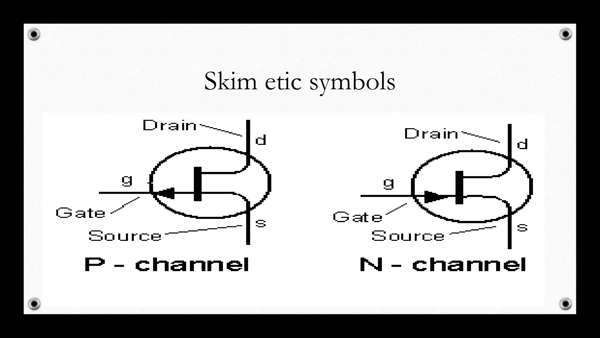
- A JFET has two P-type regions diffused into an N-type (N-channel JFET) or two N-type regions into a P-type (P-channel JFET) material to form a channel. Applying a voltage to the gate controls the channel.
- The characteristics of a