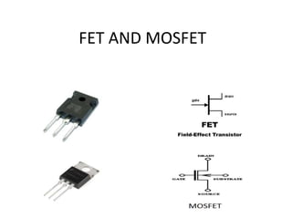
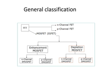
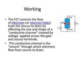
introduction, types & structure of MOSET ,turn ON and OFF of device, working, I-V characteristics of MOSFET,Different regions of operations,applications, adv & disadvantages
3. Field effect transistors
Itroduction
• Field effect devices are those in which current is controlled
by the action of an electric field, rather than carrier
injection.
• FETs are also known as unipolar transistors as they involve
single-carrier-type operation (either electron or hole).
• Field-effect transistors are so named because a weak
electrical signal coming in through one electrode creates an
electrical field through the rest of the transistor.
• FET is voltage controlled device (gate voltage controls drain
current).
• while BJT is current controlled device.
4. Structure and types
• FET is a 3 terminal device
1.drain(D) 2.source(S) 3.gate(G)
• FET is of 2 types
1.n-channel(e-)
2.p-channel(p+)
5. composition
If the channel is doped with a donor impurity, n-type material is
formed and the channel current consist of electrons.
If the channel is doped with an acceptor impurity, p-type
material will be formed and the channel current will consist of
holes.
N-channel devices have greater conductivity than p-channel
types, since electrons have higher mobility than do holes.
It is also the same for MOSFET’s.
6. Working
• The FET controls the flow
of electrons (or electron holes)
from the source to drain by
affecting the size and shape of a
"conductive channel" created by
voltage applied across the gate
and source terminals.
• This conductive channel is the
"stream" through which electrons
flow from source to drain.
7. Influence of gate voltage
• For instance consider an n-channel device.
• making the gate more positive attracts electrons
to the gate and makes the gate region thicker –
reducing the resistance of the channel. The
channel is said to be enhanced.
• making the gate more negative repels electrons
from the gate and makes the gate region thinner
– increasing the resistance of the channel. The
channel is said to be depleted.
9. APPLICATIONS
• Used in IC’S and microprocessors due to small
size.
• used as Input Amplifiers in devices such as,
Oscilloscopes, voltmeters, and other
measuring devices due to their high input
impedence.
• FETs are used in RF amplifiers for FM devices.
– Used as Current Limiter and voltage-controlled
resistors.
• Used in analogue and digital circuits.
• Used as Analog Switch.
10. Advantages and Disadvantages
• FET’s possess Very high input impedance (109-1012
)and Less Noisy.
• Very small in size, occupies very small space in Ic’s to form
circuits with a low power consumption.
• No minority carrier storage (Turn off is faster).
• It has a low gain-bandwidth .
• FETs often have a very low 'on' resistance and have a high 'off'
resistance.
• Also the amplification is very much low.
12. INTRODUCTION
• The metal oxide semiconductor field-effect
transistor is a semiconductor device which is
widely used to switch the amplification signals
in the electronic devices.
• Silicon is the main choice of semiconductor used.
• The gate is made of dielectric insulator SiO2
which has a very thin depletion layer.
13. Structure and classification
• The MOSFET is a four-
terminal device
1.source (S) 2.gate (G)
3.drain (D) 4.body (B)
• It is of two types
1.n-channel
(electrons). 2.p-channel
(holes).
14. Modes of operation
• Enhancement mode
In enhancement mode, these
are normally off and turned on by
applying gate voltage.
• Depletion mode
They are normally in on
contidion and turned off by
applying gate voltage.
15. Principle
• The MOSFET works by electronically
varying the width of a channel along
which charge carriers flow (electrons
or holes).
• The charge carriers enter the channel
at source and exit via the drain. The
width of the channel is controlled by
the voltage on an electrode called gate
located between source and drain.
• It is insulated from the channel near an
extremely thin layer of metal oxide.
16. working
• The gate electrode is placed on top of a
very thin insulating layer.
• There are a pair of small n-type regions
just under the drain & source electrodes.
• If apply a +ve voltage to gate, will push
away the ‘holes’ inside the p-type
substrate and attracts the moveable
electrons in the n-type regions under the
source & drain electrodes.
p-Si
B
VG +VDS
n-Channel
S D
17. Working of P&N channel
p-channel n-channel
It has p-channel region between source
and drain.
It has n-channel region between source
and drain.
The drain and source are heavily doped p
region and the body is n substrate
The drain and source are heavily doped
n+ region and the substrate is p-type
The current flow is due to positively
charged holes
The current flows due to flow of the
negatively charged electrons
When negative gate voltage is
applied,electrons under the oxide layer is
pushed into the body with arepulsive
force.
When a positive gate voltage the holes
present beneath the oxide layer
experiences repulsive force and the holes
are pushed downwards
The negative gate voltage also attracts
holes from p+ source and drain region in
to the channel region
The positive gate voltage also attracts
electrons from n+ source and drain region
in to the channel thus an electron rich
channel is formed
18. p-channel n-channel
Thus a hole rich channel is formed now if
a voltage between the source and the
drain is applied current flows.
now if a voltage is applied between the
source and drain.
The gate voltage controls the hole
concentration of the channel.
The gate voltage controls the electron
concentration in the channel
n-channel MOSFET is preferred over p-channel
MOSFET as the mobility of electrons are higher
than holes
19. I-V Characteristics of MOSFET
s.no Cut off mode Linear mode Saturation mode
1 VGS < Vt, where Vt is
the threshold voltage.
when VGS > Vt and
VDS < VGS − Vt
when VGS > Vt and VDS
> VGS − Vt
2 In this mode the device
is essentially off,
it operates similar to a
resistor in this mode
In this mode the switch
is on and conducting
3 , and in the ideal case
there is no current
flowing through the
device.
with a linear relation
between voltage and
current.
part of the channel is
turned off. This mode
corresponds to the
region to the right of the
dotted line, which is
called the pinch-off
voltage.
Pinch-off occurs when the MOSFET stops operating in the linear region
and saturation occurs