Downloaded 475 times

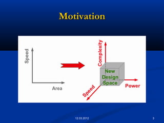


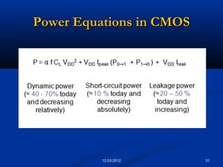
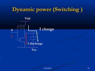
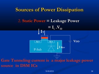
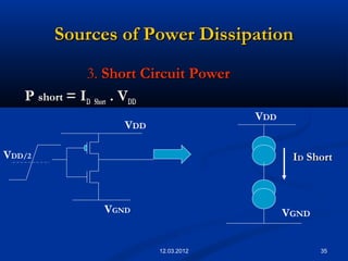


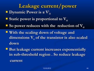
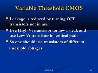


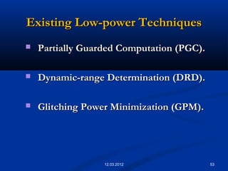
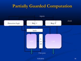
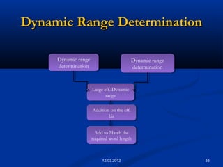


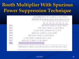


This document discusses low power VLSI design challenges and solutions. It motivates the need for low power design due to increasing power densities in VLSI chips and limited battery capacities. Sources of power dissipation in CMOS VLSI circuits are discussed including dynamic power during switching, static leakage power, and short circuit power. The document outlines various low power design methodologies at circuit, logic, architecture and software levels like reducing switching activity, glitch power reduction, gated clocking, reducing switched capacitance, using variable threshold voltages, and software optimizations.