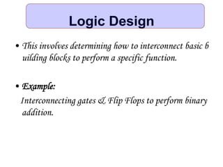
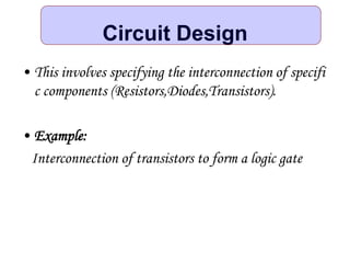
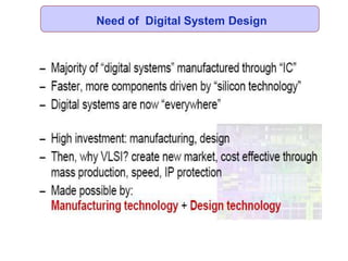
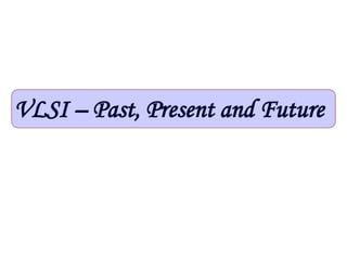
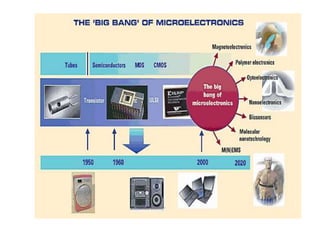
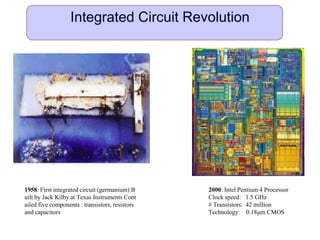
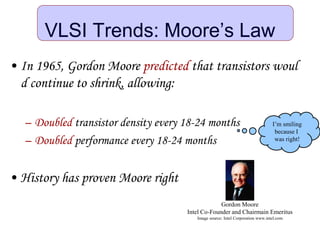
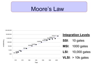
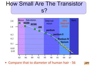
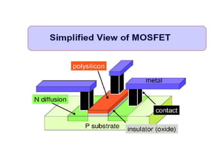
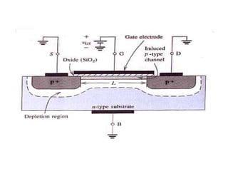
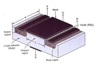
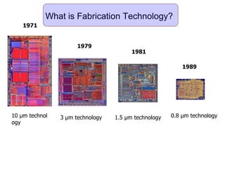
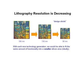
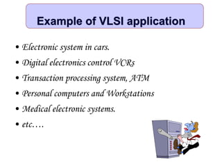
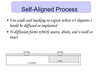
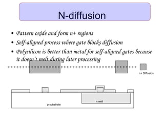
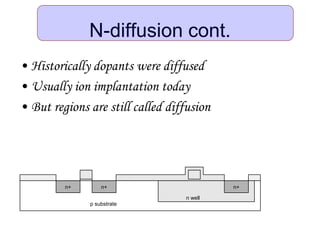
Department of Electronics & Communication Engineering
Acharya Institute of Technology, Bangalore
VLSI and its Applications
Jayalaxmi .H
Associate Proff, AIT
(jayalaxmi@acharya.ac.in)
Overview
• Why Design IC ?
• A Brief History
• Trends in VLSI
• Technical Challenges
• IC manufacturing
• CMOS Technology
• Fabrication Technology
• VLSI in everyday life
• A Look into the Future VLSI : A BIRD’ S EYE - VIEW
Why build integrated Circuit?
• Why Design IC ?
– Higher integration
•More transistors, More computing power
– Smaller and faster
– More reliable
• Advantages of IC
– Small size
•Micrometer v.s. millimeter
– Faster speed
•Smaller parasitic resistance, capacitance, and
inductance
– Less power consumption
•Smaller transistors
The advantageous of digital ICs over the
discrete components
• Size
– much smaller both transistor and wires.
• Speed
– communication within the chips are much faster than between a
chips on PCB.
– High speed of circuits on-chip due to smaller size.
• Power Consumption
– Logic operation within the chip consumes much less power.
– smaller size -> smaller parasitic capacitances and resistance -> r
equire less power to drive the circuit.
Why Digital Circuits?
The entire electronic age is based digital circuits!
Applications & S
ervices
Electronics In
dustry
Digital circui
t Industry
The First Computer:
Babbage Difference Engine
• Invented by:
Charles Babbage
• Constructed in 1832
• Built from 25,000 parts
• Cost: £17,470
ENIAC - First electronic
computer (1946)
Invention of the Transistor
• Vacuum tubes ruled in first half of 20th century Large
, expensive, power-hungry, unreliable
• 1947: first point contact transistor
– John Bardeen and Walter Brattain at Bell Labs
Transistor Types
• Bipolar transistors
– npn or pnp silicon structure
– Small current into very thin base layer controls large curre
nts between emitter and collector
– Base currents limit integration density
• Metal Oxide Semiconductor Field Effect Transistors
– nMOS and pMOS MOSFETS
– Voltage applied to insulated gate controls current between
source and drain
– Low power allows very high integration
First Integrated Circuit
• Jack Kilby (Texas Instruments) invented the first integrated circuit in 19
58
• 1970’s processes usually had only nMOS transistors
– Inexpensive, but consume power while idle
• 1980s-present: CMOS processes for low idle power
MOS Integrated Circuits
Intel 1101 256-bit SRAM Intel 4004 4-bit mProc
• CMOS remains the driving techn
ology
• A lot of chip area is memory
• Very little is completely custom
• Many blocks synthesized from V
HDL or Verilog
• Transistor count for Pentium 4 ~
50 million
• Currently implemented at 65nm t
echnology node
Modern Processors
Intel Pentium 4
Digital Systems
• Impact of Digital Systems on society.
- Instrumentation.
- Control System.
- Data Manipulation.
- Signal Processing.
- Telecommunication.
Digital Electronics Technology
• World is Digital
Digital System
A digital system is an electronic network that processes i
nformation using only digits (numbers) to implement c
alculations & operations.
Classification:
• System Design.
• Logic Design.
• Circuit Design.
System Design
• Break the overall system into subsystems & specify th
e characterstics of each subsystems.
• Example: System design of a Digital Computer.
-Number & type of memory units.
-Arithmetic unit.
-Input and Output unit.
-Control Unit.
Logic Design
• This involves determining how to interconnect basic b
uilding blocks to perform a specific function.
• Example:
Interconnecting gates & Flip Flops to perform binary
addition.
Circuit Design
• This involves specifying the interconnection of specifi
c components (Resistors,Diodes,Transistors).
• Example:
Interconnection of transistors to form a logic gate
Need of Digital System Design
VLSI – Past, Present and Future
Microelectronics Market
􀁻 Primary Market
􀁻 Information Systems
􀁻 Telecommunications
􀁻 Consumer
􀁻 Secondary Market
􀁻 Systems (e.g. Transportation)
􀁻 Manufacturing (e.g. Robots
Integrated Circuit Revolution
1958: First integrated circuit (germanium) B
uilt by Jack Kilby at Texas Instruments Cont
ailed five components : transistors, resistors
and capacitors
2000: Intel Pentium 4 Processor
Clock speed: 1.5 GHz
# Transistors: 42 million
Technology: 0.18μm CMOS
VLSI Trends: Moore’s Law
• In 1965, Gordon Moore predicted that transistors woul
d continue to shrink, allowing:
– Doubled transistor density every 18-24 months
– Doubled performance every 18-24 months
• History has proven Moore right
I’m smiling
because I
was right!
Gordon Moore
Intel Co-Founder and Chairmain Emeritus
Image source: Intel Corporation www.intel.com
Moore’s Law
Year
Transistors
4004
8008
8080
8086
80286
Intel386
Intel486
Pentium
Pentium Pro
Pentium II
Pentium III
Pentium 4
1,000
10,000
100,000
1,000,000
10,000,000
100,000,000
1,000,000,000
1970 1975 1980 1985 1990 1995 2000
Integration Levels
SSI: 10 gates
MSI: 1000 gates
LSI: 10,000 gates
VLSI: > 10k gates
Frequency
Lead Microprocessors frequency doubles every 2 years
P6
Pentium ® proc
486
386
28680868085
8080
8008
4004
0.1
1
10
100
1000
10000
1970 1980 1990 2000 2010
Year
Frequency(Mhz)
Doubles every
2 years
Evolution in IC Complexity
1) SSI – Small Scale Integration (1 – 10 logic gates)
2) MSI – Medium Scale Integration (10-100 gates)
logic functions, counters
3) LSI – Large Scale Integration (Up to 10000 gates)
first microprocessors on the chip
4) VLSI – Very Large Scale Integration (above 10000 gates)
now offers 64-bit microprocessors,
IC Evolution
How to evaluate performance of a digital circuit (gat
e, block, …)?
• Cost
• Reliability
• Scalability
• Speed (delay, operating frequency)
• Power dissipation
• Energy to perform a function
Design Metrics
How Small Are The Transistor
s?
• Compare that to diameter of human hair - 56
83 86 89 92 95 98 01 04
0.1
80286
80386
486
pentium
pentium II
1.0
0.2
0.3
2.0
0.05
Pentium IV
0.03
Itanium
07
Micron Sub-micron Deep-sub
micron
Ultra
Deep-sub
micron
Nano
mm
TREND
Complexity
How to Handle Complexity?
VLSI Design Flow
Specifications
X = AB
;
Y = CD
;
Grand Challenges
• Enhancing Performance
– Along with power dissipation in high end applications
– Leakage power in low power applications
• Cost effective manufacturing
– Reduce manufacturing costs
– Make reliable chips => Increase Yield
DESIGN CHALLENGES
Major Roadblocks Predicted
Wire Delay PowerVariability Soft Errors
Designer’s Dilemma
Area
Cost of the die.
Power
Portable application –
PCS, wireless, etc.
Speed
State-of-the-art microprocessors,
communications, etc.
?
Yield
Manufacturability
Low Power Design
• Standby Power: Drain leakage will increase as VT de
creases to maintain noise margins and meet frequency
demands, leading to excessive battery draining standb
y power consumption.
Year 2002 2005 2008 2011 2014
Power supply Vdd (V) 1.5 1.2 0.9 0.7 0.6
Threshold VT (V) 0.4 0.4 0.35 0.3 0.25
8KW
1.7KW
400W
88W
12W
0%
10%
20%
30%
40%
50%
2000 2002 2004 2006 2008
StandbyPower
…and phones leaky!
How Chips Have Shrunk
• 1946 in UPenn
• Measured in cubic ft.
 7.44 mm x 5.29 mm
 0.5 technology
ENIAC on a Chip
• 1997
• 174,569 Transistor
s
m
What is common to all these end-e
quipment?
They all power the Com
munications and Interne
t Age
They are strongly driven
by developments in Sem
iconductors
and...
VLSI Evolution
1 computer/ group of peopl
e
MAINFRAME
PERSONAL
COMPUTER
1 computer/
person
INTERNET
Few computers/
home
MOBILE
INTERNET
Many computers/
person
1970 1980 1990 2000
IC manufacturing
• IC design flow
overview
IC manufacturing
• VLSI design Funnel
Summary of VLSI Design Flow
ENTRY SYNTHESIS
VERIFICATION
QUALITY
TEST
VLSI Design Cycle
System Specification
Architectural Design
Logic Design
Circuit Design
Physical Design
Functional Design Fabrication
Packaging
MOS Transistor
• MOS Metal Oxide Silicon
– NMOS n-type transistor MOS
– PMOS p-type Transistor MOS
– CMOS complementary MOS
N Transistor Structure Review
Key feature:
transistor length L
2002: L=130nm
2003: L=90nm
2005: L=65nm?
P Transistor Structure Review
1971
1979
1989
1981
10 µm technol
ogy
3 µm technology 1.5 µm technology 0.8 µm technology
What is Fabrication Technology?
FABRICATION UNIT
Patterning of SiO2 – Cross Section
Si-substrate
Si-substrate Si-substrate
(a) Silicon base material
(b) After oxidation and deposition
of negative photoresist
(c) Stepper exposure
Photoresist
SiO
2
UV-light
Patterned
optical mask
Exposed resist
SiO
2
Si-substrate
Si-substrate
Si-substrate
SiO
2
SiO
2
(d) After development and etching of resist,
chemical or plasma etch of SiO
2
(e) After etching
(f) Final result after removal of resist
Hardened resist
Hardened resist
Chemical or plasma
etch
oxidation
optical
mask
process
step
photoresist coatingphotoresist
removal (ashing)
spin, rinse, dry
photoresist
stepper exposure
development
acid etch
Photo-Lithographic Process
Computer Aided Design
• Why do we need CAD tool?
– complexity of circuit
• CAD TOOLs
– Design Tool
• ie. schematic drawing packages
– Analysis and Verification Tool
• ie. SPICE
– Syntesis Tool
• generate low level of abstraction
A View of the Clean room
0.25 micron transistor (Bell Labs)
poly
silicide
source/drain
gate oxide
Emerging Structures..
Example of VLSI application
• Electronic system in cars.
• Digital electronics control VCRs
• Transaction processing system, ATM
• Personal computers and Workstations
• Medical electronic systems.
• etc….
Applications
MP3 Player
Fabrication Steps
• Start with blank wafer
• Build inverter from the bottom up
• First step will be to form the n-well
– Cover wafer with protective layer of SiO2 (oxide)
– Remove layer where n-well should be built
– Implant or diffuse n dopants into exposed wafer
– Strip off SiO2
p substrate
Oxidation
• Grow SiO2 on top of Si wafer
– 900 – 1200 C with H2O or O2 in oxidation furnace
p substrate
SiO2
Photoresist
• Spin on photoresist
– Photoresist is a light-sensitive organic polymer
– Softens where exposed to light
p substrate
SiO2
Photoresist
Lithography
• Expose photoresist through n-well mask
• Strip off exposed photoresist
p substrate
SiO2
Photoresist
Etch
• Etch oxide with hydrofluoric acid (HF)
– Seeps through skin and eats bone; nasty stuff!!!
• Only attacks oxide where resist has been exposed
p substrate
SiO2
Photoresist
Strip Photoresist
• Strip off remaining photoresist
– Use mixture of acids called piranah etch
• Necessary so resist doesn’t melt in next step
p substrate
SiO2
n-well
• n-well is formed with diffusion or ion implantation
• Diffusion
– Place wafer in furnace with arsenic gas
– Heat until As atoms diffuse into exposed Si
• Ion Implanatation
– Blast wafer with beam of As ions
– Ions blocked by SiO2, only enter exposed Si
n well
SiO2
Strip Oxide
• Strip off the remaining oxide using HF
• Back to bare wafer with n-well
• Subsequent steps involve similar series of steps
p substrate
n well
Polysilicon
• Deposit very thin layer of gate oxide
– < 20 Å (6-7 atomic layers)
• Chemical Vapor Deposition (CVD) of silicon layer
– Place wafer in furnace with Silane gas (SiH4)
– Forms many small crystals called polysilicon
– Heavily doped to be good conductor
Thin gate oxide
Polysilicon
p substrate
n well
Polysilicon Patterning
• Use same lithography process to pattern polysilicon
Polysilicon
p substrate
Thin gate oxide
Polysilicon
n well
Self-Aligned Process
• Use oxide and masking to expose where n+ dopants s
hould be diffused or implanted
• N-diffusion forms nMOS source, drain, and n-well co
ntact
p substrate
n well
N-diffusion
• Pattern oxide and form n+ regions
• Self-aligned process where gate blocks diffusion
• Polysilicon is better than metal for self-aligned gates because
it doesn’t melt during later processing
p substrate
n well
n+ Diffusion
N-diffusion cont.
• Historically dopants were diffused
• Usually ion implantation today
• But regions are still called diffusion
n well
p substrate
n+n+ n+
-A way of thinking which seeks changes in perceptions, concepts, and i
deas through the use of formal thinking tools
(Edward de Bono)

basic vlsi ppt

  • 1.
    Department of Electronics& Communication Engineering Acharya Institute of Technology, Bangalore VLSI and its Applications Jayalaxmi .H Associate Proff, AIT (jayalaxmi@acharya.ac.in)
  • 2.
    Overview • Why DesignIC ? • A Brief History • Trends in VLSI • Technical Challenges • IC manufacturing • CMOS Technology • Fabrication Technology • VLSI in everyday life • A Look into the Future VLSI : A BIRD’ S EYE - VIEW
  • 3.
    Why build integratedCircuit? • Why Design IC ? – Higher integration •More transistors, More computing power – Smaller and faster – More reliable • Advantages of IC – Small size •Micrometer v.s. millimeter – Faster speed •Smaller parasitic resistance, capacitance, and inductance – Less power consumption •Smaller transistors
  • 4.
    The advantageous ofdigital ICs over the discrete components • Size – much smaller both transistor and wires. • Speed – communication within the chips are much faster than between a chips on PCB. – High speed of circuits on-chip due to smaller size. • Power Consumption – Logic operation within the chip consumes much less power. – smaller size -> smaller parasitic capacitances and resistance -> r equire less power to drive the circuit.
  • 5.
    Why Digital Circuits? Theentire electronic age is based digital circuits! Applications & S ervices Electronics In dustry Digital circui t Industry
  • 6.
    The First Computer: BabbageDifference Engine • Invented by: Charles Babbage • Constructed in 1832 • Built from 25,000 parts • Cost: £17,470
  • 7.
    ENIAC - Firstelectronic computer (1946)
  • 8.
    Invention of theTransistor • Vacuum tubes ruled in first half of 20th century Large , expensive, power-hungry, unreliable • 1947: first point contact transistor – John Bardeen and Walter Brattain at Bell Labs
  • 9.
    Transistor Types • Bipolartransistors – npn or pnp silicon structure – Small current into very thin base layer controls large curre nts between emitter and collector – Base currents limit integration density • Metal Oxide Semiconductor Field Effect Transistors – nMOS and pMOS MOSFETS – Voltage applied to insulated gate controls current between source and drain – Low power allows very high integration
  • 10.
    First Integrated Circuit •Jack Kilby (Texas Instruments) invented the first integrated circuit in 19 58
  • 11.
    • 1970’s processesusually had only nMOS transistors – Inexpensive, but consume power while idle • 1980s-present: CMOS processes for low idle power MOS Integrated Circuits Intel 1101 256-bit SRAM Intel 4004 4-bit mProc
  • 12.
    • CMOS remainsthe driving techn ology • A lot of chip area is memory • Very little is completely custom • Many blocks synthesized from V HDL or Verilog • Transistor count for Pentium 4 ~ 50 million • Currently implemented at 65nm t echnology node Modern Processors Intel Pentium 4
  • 13.
    Digital Systems • Impactof Digital Systems on society. - Instrumentation. - Control System. - Data Manipulation. - Signal Processing. - Telecommunication.
  • 14.
  • 15.
    Digital System A digitalsystem is an electronic network that processes i nformation using only digits (numbers) to implement c alculations & operations. Classification: • System Design. • Logic Design. • Circuit Design.
  • 16.
    System Design • Breakthe overall system into subsystems & specify th e characterstics of each subsystems. • Example: System design of a Digital Computer. -Number & type of memory units. -Arithmetic unit. -Input and Output unit. -Control Unit.
  • 17.
    Logic Design • Thisinvolves determining how to interconnect basic b uilding blocks to perform a specific function. • Example: Interconnecting gates & Flip Flops to perform binary addition.
  • 18.
    Circuit Design • Thisinvolves specifying the interconnection of specifi c components (Resistors,Diodes,Transistors). • Example: Interconnection of transistors to form a logic gate
  • 19.
    Need of DigitalSystem Design
  • 20.
    VLSI – Past,Present and Future
  • 21.
    Microelectronics Market 􀁻 PrimaryMarket 􀁻 Information Systems 􀁻 Telecommunications 􀁻 Consumer 􀁻 Secondary Market 􀁻 Systems (e.g. Transportation) 􀁻 Manufacturing (e.g. Robots
  • 22.
    Integrated Circuit Revolution 1958:First integrated circuit (germanium) B uilt by Jack Kilby at Texas Instruments Cont ailed five components : transistors, resistors and capacitors 2000: Intel Pentium 4 Processor Clock speed: 1.5 GHz # Transistors: 42 million Technology: 0.18μm CMOS
  • 23.
    VLSI Trends: Moore’sLaw • In 1965, Gordon Moore predicted that transistors woul d continue to shrink, allowing: – Doubled transistor density every 18-24 months – Doubled performance every 18-24 months • History has proven Moore right I’m smiling because I was right! Gordon Moore Intel Co-Founder and Chairmain Emeritus Image source: Intel Corporation www.intel.com
  • 24.
    Moore’s Law Year Transistors 4004 8008 8080 8086 80286 Intel386 Intel486 Pentium Pentium Pro PentiumII Pentium III Pentium 4 1,000 10,000 100,000 1,000,000 10,000,000 100,000,000 1,000,000,000 1970 1975 1980 1985 1990 1995 2000 Integration Levels SSI: 10 gates MSI: 1000 gates LSI: 10,000 gates VLSI: > 10k gates
  • 25.
    Frequency Lead Microprocessors frequencydoubles every 2 years P6 Pentium ® proc 486 386 28680868085 8080 8008 4004 0.1 1 10 100 1000 10000 1970 1980 1990 2000 2010 Year Frequency(Mhz) Doubles every 2 years
  • 26.
    Evolution in ICComplexity
  • 27.
    1) SSI –Small Scale Integration (1 – 10 logic gates) 2) MSI – Medium Scale Integration (10-100 gates) logic functions, counters 3) LSI – Large Scale Integration (Up to 10000 gates) first microprocessors on the chip 4) VLSI – Very Large Scale Integration (above 10000 gates) now offers 64-bit microprocessors, IC Evolution
  • 28.
    How to evaluateperformance of a digital circuit (gat e, block, …)? • Cost • Reliability • Scalability • Speed (delay, operating frequency) • Power dissipation • Energy to perform a function Design Metrics
  • 29.
    How Small AreThe Transistor s? • Compare that to diameter of human hair - 56 83 86 89 92 95 98 01 04 0.1 80286 80386 486 pentium pentium II 1.0 0.2 0.3 2.0 0.05 Pentium IV 0.03 Itanium 07 Micron Sub-micron Deep-sub micron Ultra Deep-sub micron Nano mm
  • 30.
  • 31.
  • 32.
    How to HandleComplexity?
  • 33.
  • 34.
    Grand Challenges • EnhancingPerformance – Along with power dissipation in high end applications – Leakage power in low power applications • Cost effective manufacturing – Reduce manufacturing costs – Make reliable chips => Increase Yield
  • 35.
  • 36.
    Major Roadblocks Predicted WireDelay PowerVariability Soft Errors
  • 37.
    Designer’s Dilemma Area Cost ofthe die. Power Portable application – PCS, wireless, etc. Speed State-of-the-art microprocessors, communications, etc. ? Yield Manufacturability
  • 38.
    Low Power Design •Standby Power: Drain leakage will increase as VT de creases to maintain noise margins and meet frequency demands, leading to excessive battery draining standb y power consumption. Year 2002 2005 2008 2011 2014 Power supply Vdd (V) 1.5 1.2 0.9 0.7 0.6 Threshold VT (V) 0.4 0.4 0.35 0.3 0.25 8KW 1.7KW 400W 88W 12W 0% 10% 20% 30% 40% 50% 2000 2002 2004 2006 2008 StandbyPower …and phones leaky!
  • 39.
    How Chips HaveShrunk • 1946 in UPenn • Measured in cubic ft.
  • 40.
     7.44 mmx 5.29 mm  0.5 technology ENIAC on a Chip • 1997 • 174,569 Transistor s m
  • 41.
    What is commonto all these end-e quipment? They all power the Com munications and Interne t Age They are strongly driven by developments in Sem iconductors and...
  • 42.
    VLSI Evolution 1 computer/group of peopl e MAINFRAME PERSONAL COMPUTER 1 computer/ person INTERNET Few computers/ home MOBILE INTERNET Many computers/ person 1970 1980 1990 2000
  • 43.
    IC manufacturing • ICdesign flow overview
  • 44.
  • 48.
    Summary of VLSIDesign Flow ENTRY SYNTHESIS VERIFICATION QUALITY TEST
  • 49.
    VLSI Design Cycle SystemSpecification Architectural Design Logic Design Circuit Design Physical Design Functional Design Fabrication Packaging
  • 50.
    MOS Transistor • MOSMetal Oxide Silicon – NMOS n-type transistor MOS – PMOS p-type Transistor MOS – CMOS complementary MOS
  • 51.
  • 52.
    Key feature: transistor lengthL 2002: L=130nm 2003: L=90nm 2005: L=65nm? P Transistor Structure Review
  • 56.
    1971 1979 1989 1981 10 µm technol ogy 3µm technology 1.5 µm technology 0.8 µm technology What is Fabrication Technology?
  • 57.
  • 58.
    Patterning of SiO2– Cross Section Si-substrate Si-substrate Si-substrate (a) Silicon base material (b) After oxidation and deposition of negative photoresist (c) Stepper exposure Photoresist SiO 2 UV-light Patterned optical mask Exposed resist SiO 2 Si-substrate Si-substrate Si-substrate SiO 2 SiO 2 (d) After development and etching of resist, chemical or plasma etch of SiO 2 (e) After etching (f) Final result after removal of resist Hardened resist Hardened resist Chemical or plasma etch
  • 59.
    oxidation optical mask process step photoresist coatingphotoresist removal (ashing) spin,rinse, dry photoresist stepper exposure development acid etch Photo-Lithographic Process
  • 61.
    Computer Aided Design •Why do we need CAD tool? – complexity of circuit • CAD TOOLs – Design Tool • ie. schematic drawing packages – Analysis and Verification Tool • ie. SPICE – Syntesis Tool • generate low level of abstraction
  • 62.
    A View ofthe Clean room
  • 63.
    0.25 micron transistor(Bell Labs) poly silicide source/drain gate oxide
  • 64.
  • 65.
    Example of VLSIapplication • Electronic system in cars. • Digital electronics control VCRs • Transaction processing system, ATM • Personal computers and Workstations • Medical electronic systems. • etc….
  • 66.
  • 67.
  • 68.
    Fabrication Steps • Startwith blank wafer • Build inverter from the bottom up • First step will be to form the n-well – Cover wafer with protective layer of SiO2 (oxide) – Remove layer where n-well should be built – Implant or diffuse n dopants into exposed wafer – Strip off SiO2 p substrate
  • 69.
    Oxidation • Grow SiO2on top of Si wafer – 900 – 1200 C with H2O or O2 in oxidation furnace p substrate SiO2
  • 70.
    Photoresist • Spin onphotoresist – Photoresist is a light-sensitive organic polymer – Softens where exposed to light p substrate SiO2 Photoresist
  • 71.
    Lithography • Expose photoresistthrough n-well mask • Strip off exposed photoresist p substrate SiO2 Photoresist
  • 72.
    Etch • Etch oxidewith hydrofluoric acid (HF) – Seeps through skin and eats bone; nasty stuff!!! • Only attacks oxide where resist has been exposed p substrate SiO2 Photoresist
  • 73.
    Strip Photoresist • Stripoff remaining photoresist – Use mixture of acids called piranah etch • Necessary so resist doesn’t melt in next step p substrate SiO2
  • 74.
    n-well • n-well isformed with diffusion or ion implantation • Diffusion – Place wafer in furnace with arsenic gas – Heat until As atoms diffuse into exposed Si • Ion Implanatation – Blast wafer with beam of As ions – Ions blocked by SiO2, only enter exposed Si n well SiO2
  • 75.
    Strip Oxide • Stripoff the remaining oxide using HF • Back to bare wafer with n-well • Subsequent steps involve similar series of steps p substrate n well
  • 76.
    Polysilicon • Deposit verythin layer of gate oxide – < 20 Å (6-7 atomic layers) • Chemical Vapor Deposition (CVD) of silicon layer – Place wafer in furnace with Silane gas (SiH4) – Forms many small crystals called polysilicon – Heavily doped to be good conductor Thin gate oxide Polysilicon p substrate n well
  • 77.
    Polysilicon Patterning • Usesame lithography process to pattern polysilicon Polysilicon p substrate Thin gate oxide Polysilicon n well
  • 78.
    Self-Aligned Process • Useoxide and masking to expose where n+ dopants s hould be diffused or implanted • N-diffusion forms nMOS source, drain, and n-well co ntact p substrate n well
  • 79.
    N-diffusion • Pattern oxideand form n+ regions • Self-aligned process where gate blocks diffusion • Polysilicon is better than metal for self-aligned gates because it doesn’t melt during later processing p substrate n well n+ Diffusion
  • 80.
    N-diffusion cont. • Historicallydopants were diffused • Usually ion implantation today • But regions are still called diffusion n well p substrate n+n+ n+
  • 81.
    -A way ofthinking which seeks changes in perceptions, concepts, and i deas through the use of formal thinking tools (Edward de Bono)