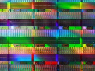
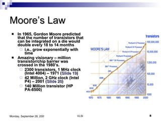
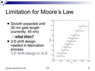
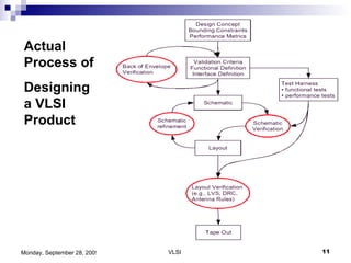
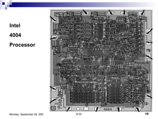
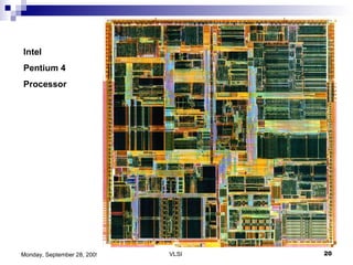
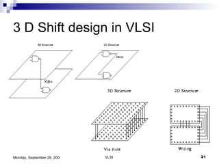
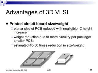
Think about it.. On previous slide you saw some picture, that was the processor of a computer and the image was from Intel Lab. The zooming size was of scale of a rabies virus, that's the technology we are dealing today!
Basics of Very Large Scale Integration  (VLSI) Compiled By- Agarwal Avanish Iyer Makesh Desai Tejas Lokhande Sanket
Includes.. Introduction What is VLSI? Moore’s Law VLSI Design- Introduction Synthesis Flow Advantages Disadvantages Applications Reference
Introduction Microprocessors are essential to many of the products we use every day such as TVs, cars, radios, home appliances and of course, computers. Transistors are the main components of microprocessors. At their most basic level, transistors may seem simple. But their development actually required many years of painstaking research. Before transistors, computers relied on slow, inefficient vacuum tubes and mechanical switches to process information. In 1958, engineers   managed to put two transistors onto a  Silicon  crystal and create the first integrated circuit, which  subsequently  led to the  first  microprocessor. 
Major Challenge Microscopic issues ultra-high speeds power dissipation and supply rail drop growing importance of interconnect noise, crosstalk reliability, manufacturability clock distribution Macroscopic issues time-to-market design complexity (millions of gates) high levels of abstractions design for test reuse and IP, portability
What is VLSI? What is VLSI? – “ Very Large Scale Integration” –  Defines integration level –  1980s hold-over from outdated taxonomy for integration levels •  Obviously influenced from frequency bands, i.e. HF, VHF, UHF –  Sources disagree on what is measured (gates or transistors?) •  SSI – Small-Scale Integration (0-102) •  MSI – Medium-Scale Integration (102 -103) •  LSI – Large-Scale Integration (103 -105) •  VLSI – Very Large-Scale Integration (105 - 107) •  ULSI – Ultra Large-Scale Integration (>= 107)
Moore’s Law In 1965, Gordon Moore predicted that the number of transistors that can be integrated on a die would double every 18 to 14 months i.e., grow exponentially with time Amazing visionary – million transistor/chip barrier was crossed in the 1980’s. 2300 transistors, 1 MHz clock (Intel 4004) – 1971 ( Slide 19 ) 42 Million, 2 GHz clock (Intel P4) – 2001 ( Slide 20 ) 140 Million transistor (HP PA-8500)
Limitation for Moore’s Law Growth expected until 30 nm gate length (currently: 45 nm) what then? 3 D shift design needed in fabrication process  3 D Shift design in VLSI
Synthesis flow- Latest 45 nm by Intel
Actual Process of Designing a VLSI Product
Advantages Compactness Mobility Reliability  Less power consumption Effective use of space Easily available productivity Large market background
Disadvantages Previously the cost was high Still the basic things like mobile phones and other related things are cheaper but high end products are pocket eater  Advancement in Indian market is required Lack of training institute so affects on production in India
India's Contribution to VLSI Indian Institute of Technology and Intel together are working for bringing advancement in VLSI to India Lot of conferences on VLSI are going in India every month and the organization named VLSI Society of India working with industry and upcoming engineer providing finance for their projects in VLSI The Indian government has launched a VLSI education program across 32 institutes to increase the availability of chip design talent. The $10 million, five-year program is meant to supplement a similar program launched in the late 1990s.  VLSI news.shtml
Applications- Daily life prospective There are so many applications in our daily life. From a simple mobile phone to the server used in large companies. Recent example is Intel's new upcoming 45 nm integration processor  The low power design in VLSI is upcoming trend in this industry
References  VLSI Society of India Chapters and news releases  www.cnet.com www.wikipedia.com www.googleimages.com www.intel.in/sponcersoftomorrow.in www.youtube.in
Please give us your valuable feedback … Thank You!
 
Intel 4004  Processor
Intel Pentium 4 Processor
3 D Shift design in VLSI
Advantages of 3D VLSI Printed circuit board size/weight planar size of PCB reduced with negligible IC height increase weight reduction due to more circuitry per package/smaller PCBs estimated 40-50 times reduction in size/weight

Basics Of VLSI

  • 1.
  • 2.
    Think about it..On previous slide you saw some picture, that was the processor of a computer and the image was from Intel Lab. The zooming size was of scale of a rabies virus, that's the technology we are dealing today!
  • 3.
    Basics of VeryLarge Scale Integration (VLSI) Compiled By- Agarwal Avanish Iyer Makesh Desai Tejas Lokhande Sanket
  • 4.
    Includes.. Introduction Whatis VLSI? Moore’s Law VLSI Design- Introduction Synthesis Flow Advantages Disadvantages Applications Reference
  • 5.
    Introduction Microprocessors areessential to many of the products we use every day such as TVs, cars, radios, home appliances and of course, computers. Transistors are the main components of microprocessors. At their most basic level, transistors may seem simple. But their development actually required many years of painstaking research. Before transistors, computers relied on slow, inefficient vacuum tubes and mechanical switches to process information. In 1958, engineers managed to put two transistors onto a Silicon crystal and create the first integrated circuit, which subsequently led to the first microprocessor. 
  • 6.
    Major Challenge Microscopicissues ultra-high speeds power dissipation and supply rail drop growing importance of interconnect noise, crosstalk reliability, manufacturability clock distribution Macroscopic issues time-to-market design complexity (millions of gates) high levels of abstractions design for test reuse and IP, portability
  • 7.
    What is VLSI?What is VLSI? – “ Very Large Scale Integration” – Defines integration level – 1980s hold-over from outdated taxonomy for integration levels • Obviously influenced from frequency bands, i.e. HF, VHF, UHF – Sources disagree on what is measured (gates or transistors?) • SSI – Small-Scale Integration (0-102) • MSI – Medium-Scale Integration (102 -103) • LSI – Large-Scale Integration (103 -105) • VLSI – Very Large-Scale Integration (105 - 107) • ULSI – Ultra Large-Scale Integration (>= 107)
  • 8.
    Moore’s Law In1965, Gordon Moore predicted that the number of transistors that can be integrated on a die would double every 18 to 14 months i.e., grow exponentially with time Amazing visionary – million transistor/chip barrier was crossed in the 1980’s. 2300 transistors, 1 MHz clock (Intel 4004) – 1971 ( Slide 19 ) 42 Million, 2 GHz clock (Intel P4) – 2001 ( Slide 20 ) 140 Million transistor (HP PA-8500)
  • 9.
    Limitation for Moore’sLaw Growth expected until 30 nm gate length (currently: 45 nm) what then? 3 D shift design needed in fabrication process 3 D Shift design in VLSI
  • 10.
    Synthesis flow- Latest45 nm by Intel
  • 11.
    Actual Process ofDesigning a VLSI Product
  • 12.
    Advantages Compactness MobilityReliability Less power consumption Effective use of space Easily available productivity Large market background
  • 13.
    Disadvantages Previously thecost was high Still the basic things like mobile phones and other related things are cheaper but high end products are pocket eater Advancement in Indian market is required Lack of training institute so affects on production in India
  • 14.
    India's Contribution toVLSI Indian Institute of Technology and Intel together are working for bringing advancement in VLSI to India Lot of conferences on VLSI are going in India every month and the organization named VLSI Society of India working with industry and upcoming engineer providing finance for their projects in VLSI The Indian government has launched a VLSI education program across 32 institutes to increase the availability of chip design talent. The $10 million, five-year program is meant to supplement a similar program launched in the late 1990s. VLSI news.shtml
  • 15.
    Applications- Daily lifeprospective There are so many applications in our daily life. From a simple mobile phone to the server used in large companies. Recent example is Intel's new upcoming 45 nm integration processor The low power design in VLSI is upcoming trend in this industry
  • 16.
    References VLSISociety of India Chapters and news releases www.cnet.com www.wikipedia.com www.googleimages.com www.intel.in/sponcersoftomorrow.in www.youtube.in
  • 17.
    Please give usyour valuable feedback … Thank You!
  • 18.
  • 19.
    Intel 4004 Processor
  • 20.
    Intel Pentium 4Processor
  • 21.
    3 D Shiftdesign in VLSI
  • 22.
    Advantages of 3DVLSI Printed circuit board size/weight planar size of PCB reduced with negligible IC height increase weight reduction due to more circuitry per package/smaller PCBs estimated 40-50 times reduction in size/weight