Downloaded 160 times

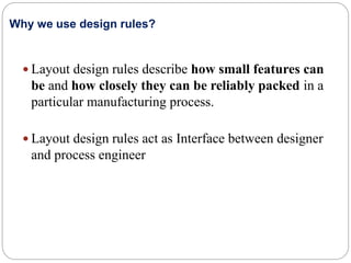

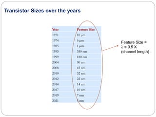

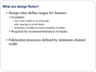


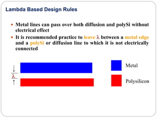


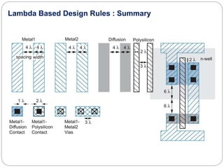


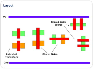


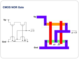


The document discusses layout design rules in semiconductor manufacturing, highlighting their role in defining the relationship between various circuit features, particularly in field-effect transistors. It outlines different approaches to design rules, such as micron rules and lambda-based rules, explaining their advantages and disadvantages in terms of feature sizes, spacing, and process control. Additionally, it provides specific design rules for different layers including metal, diffusion, and polysilicon, aimed at avoiding issues such as shorts and ensuring compatible circuit designs.