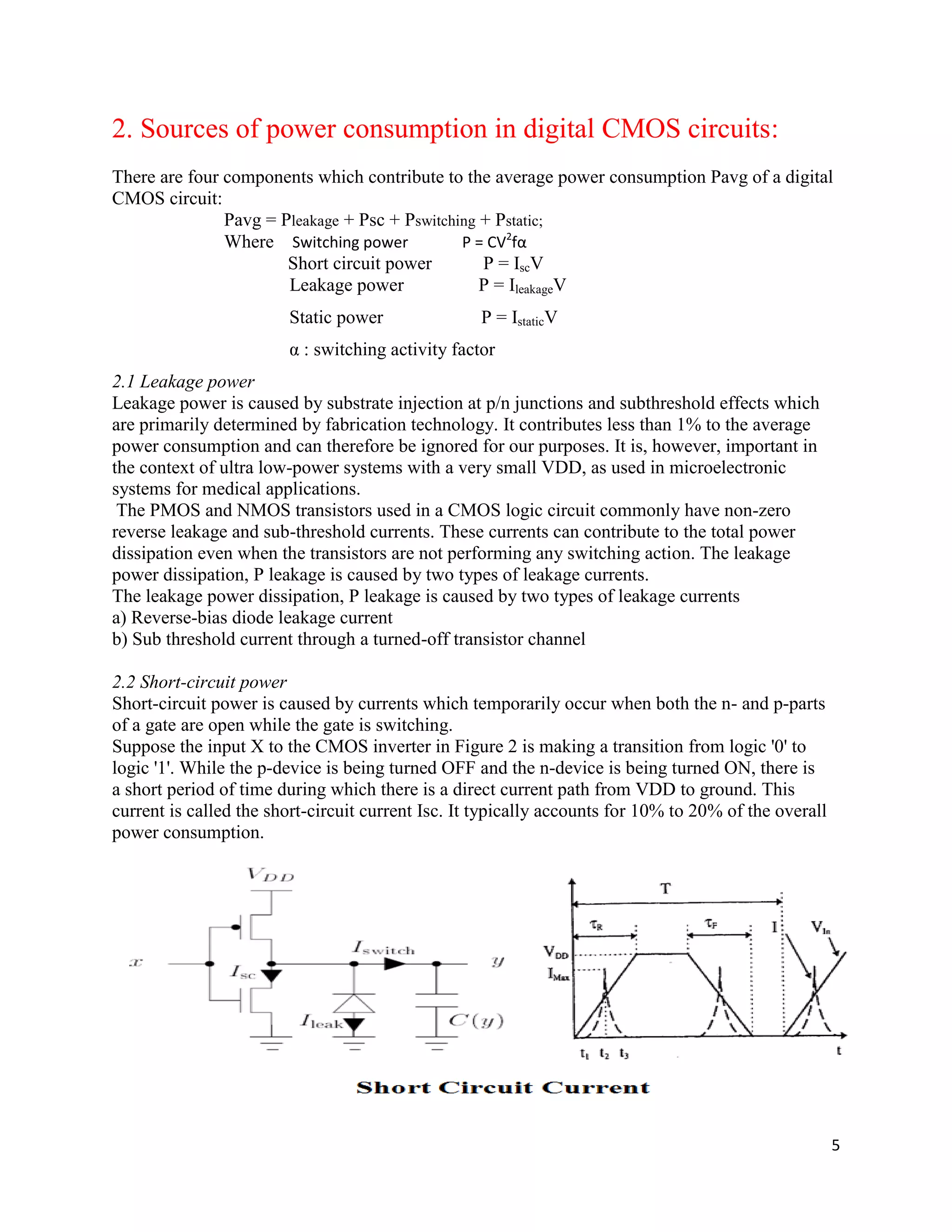
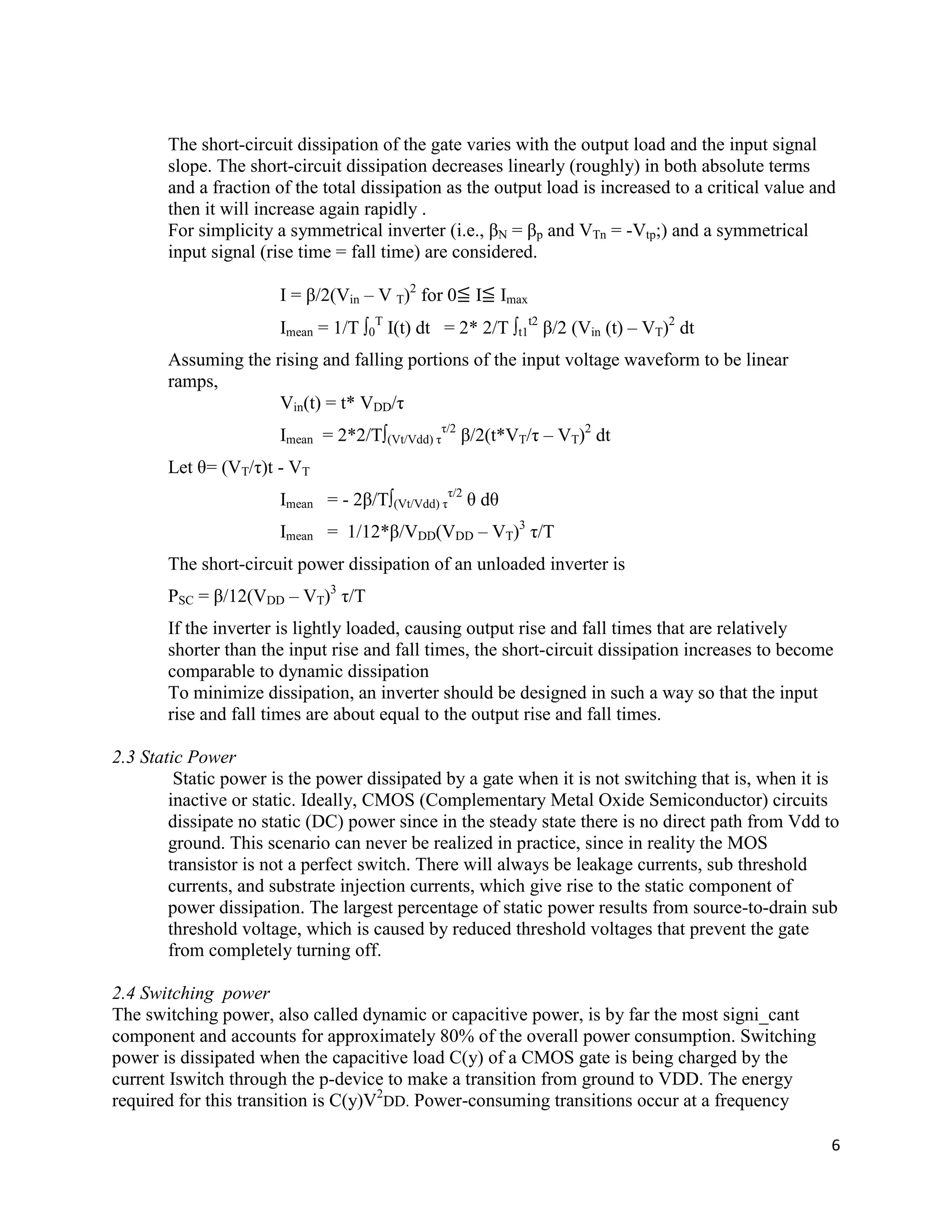
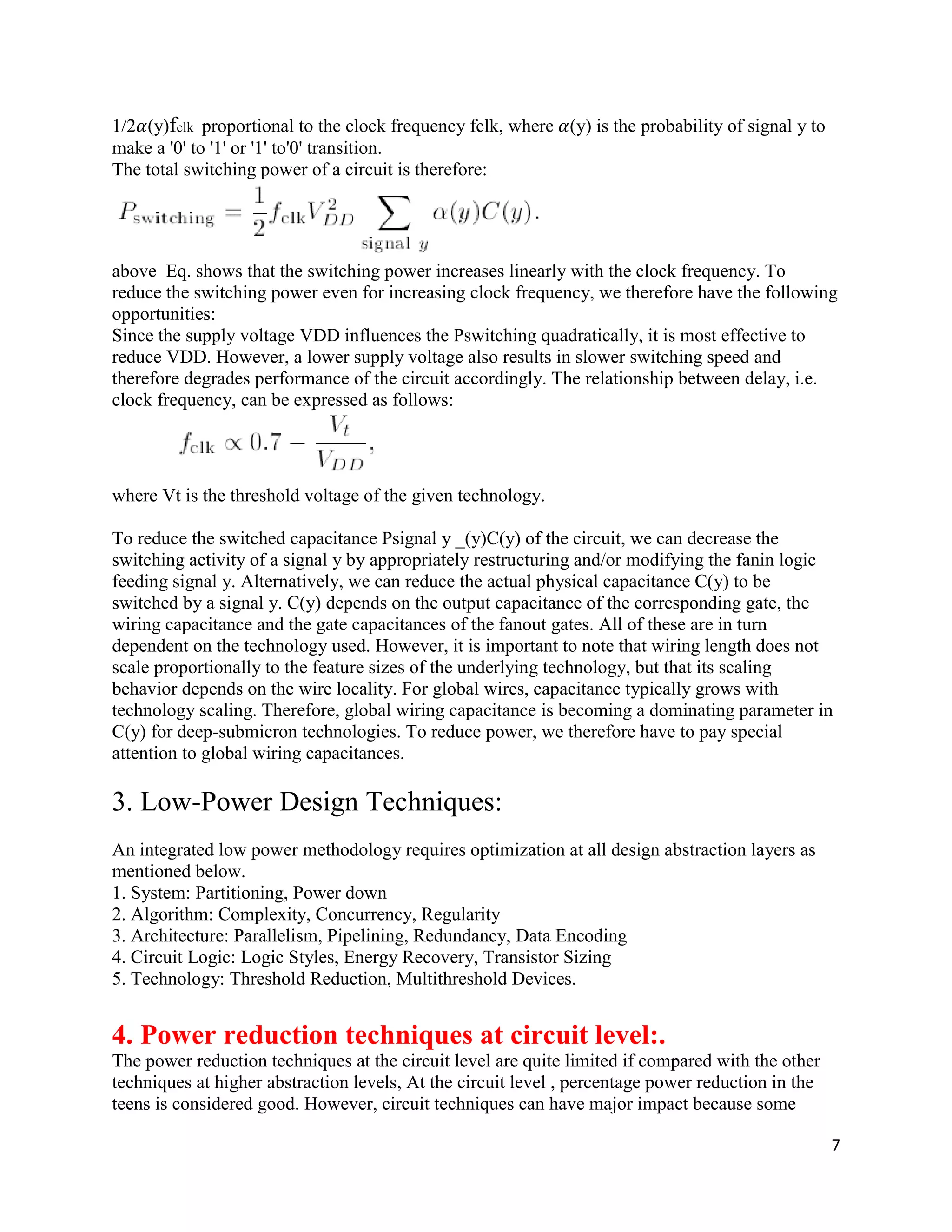
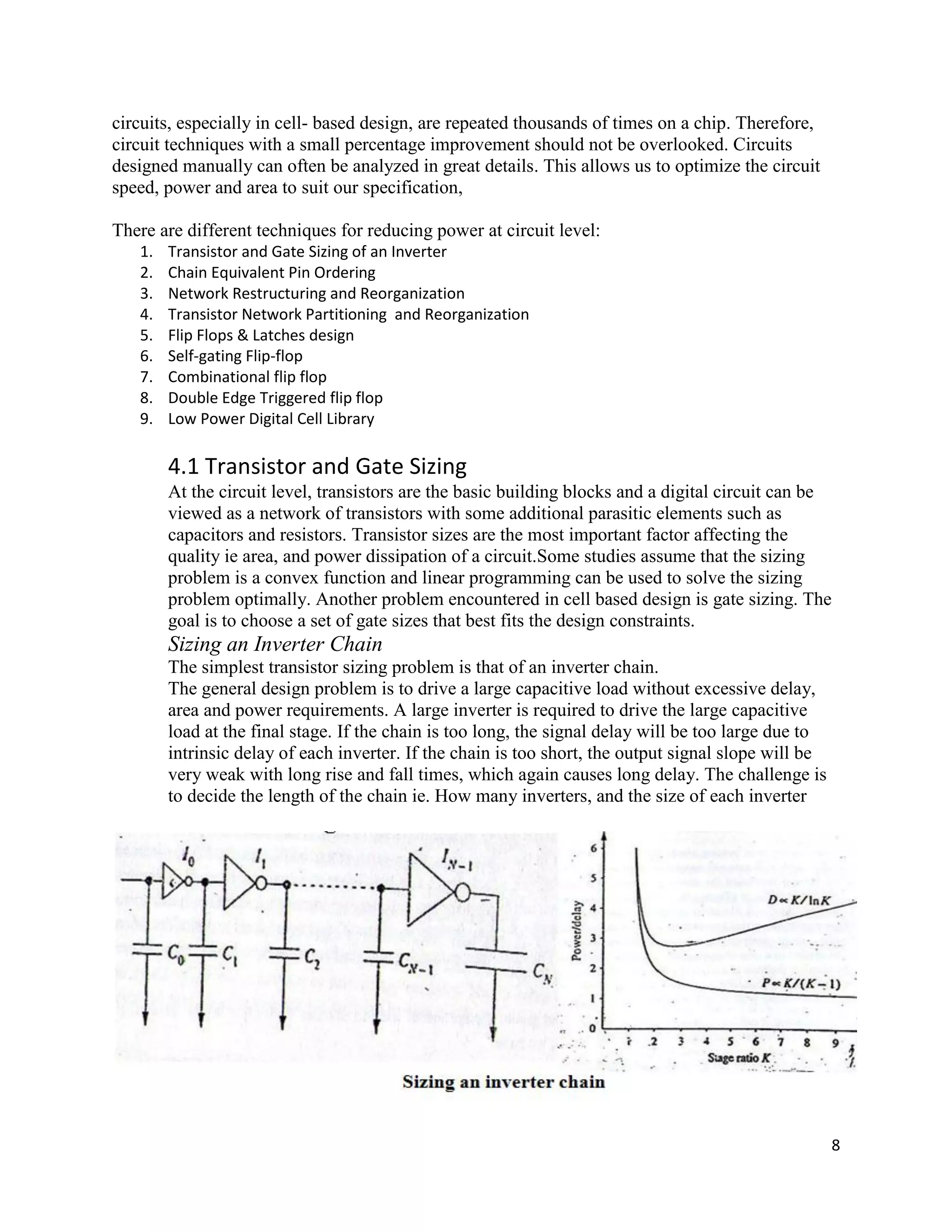
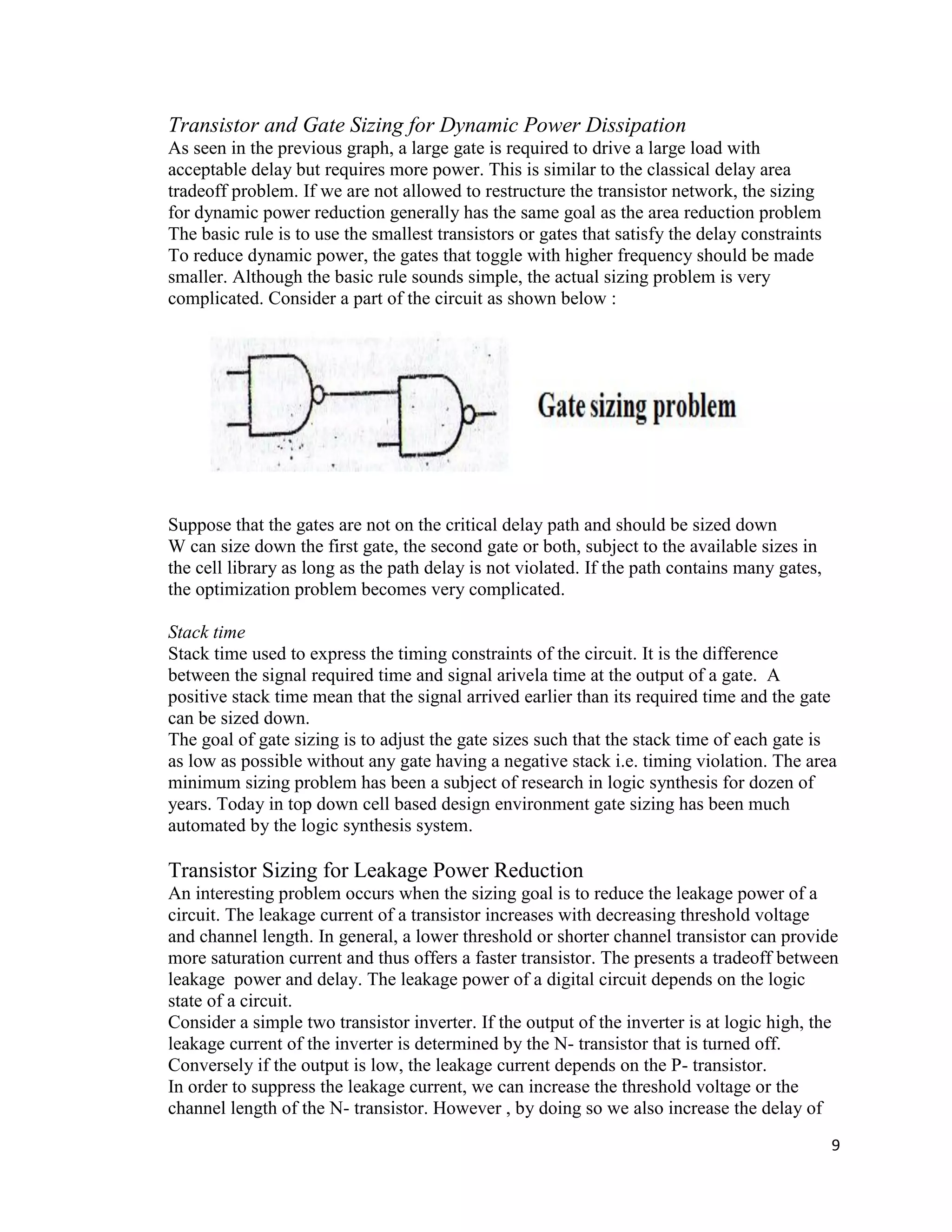
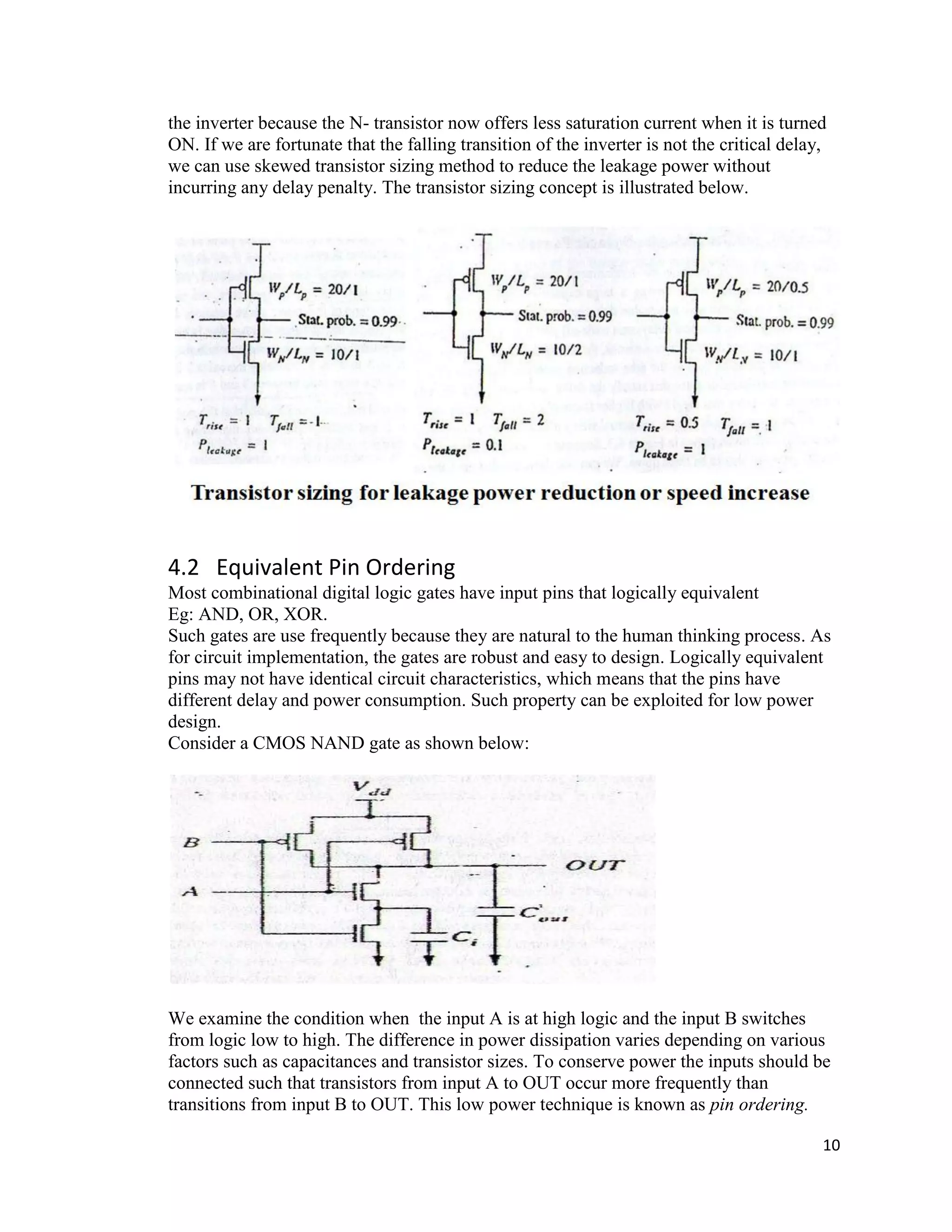
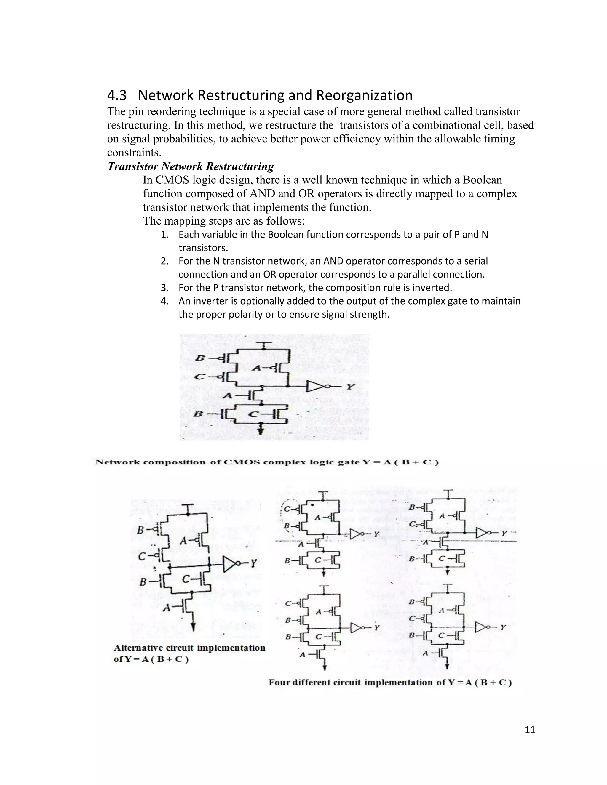
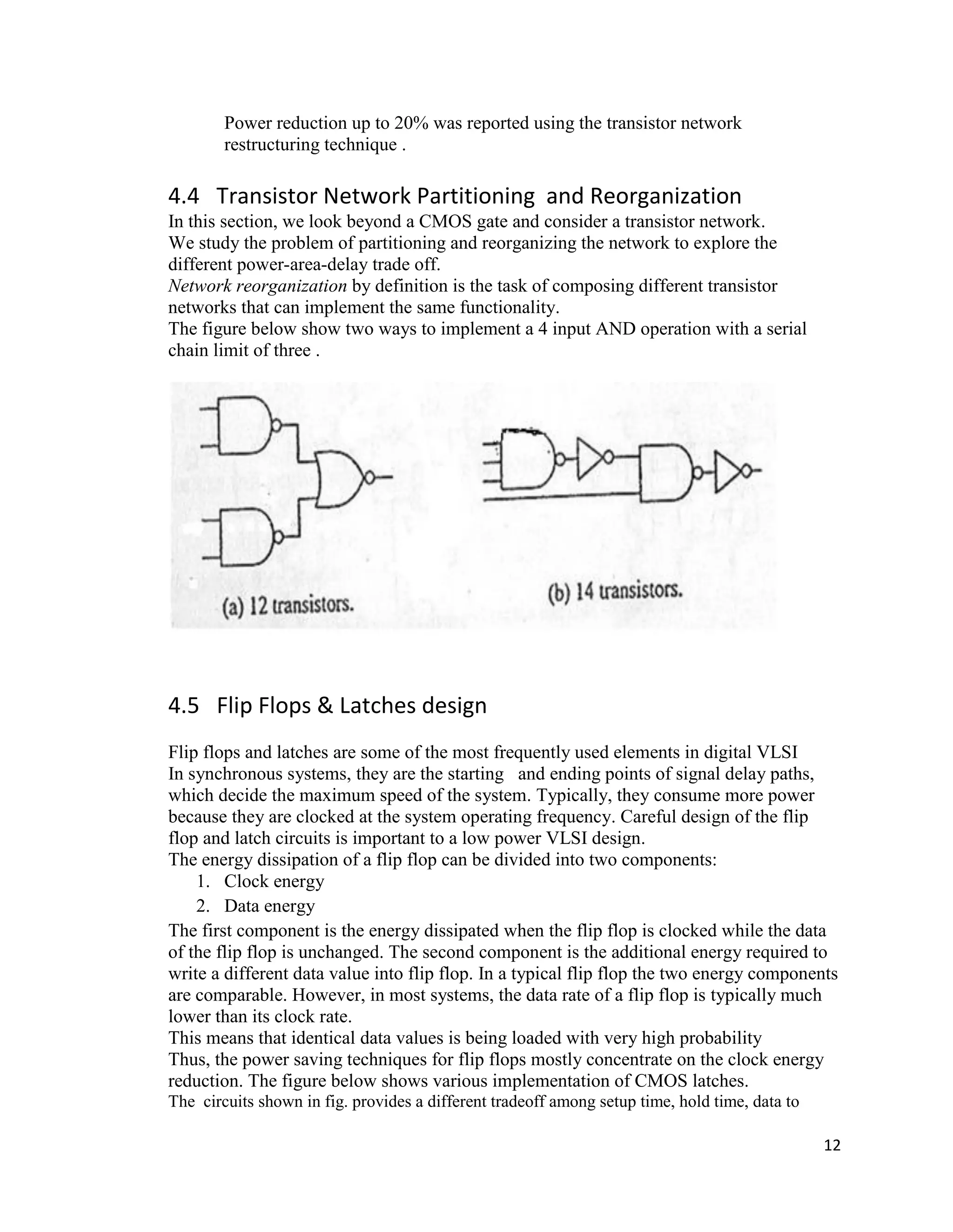
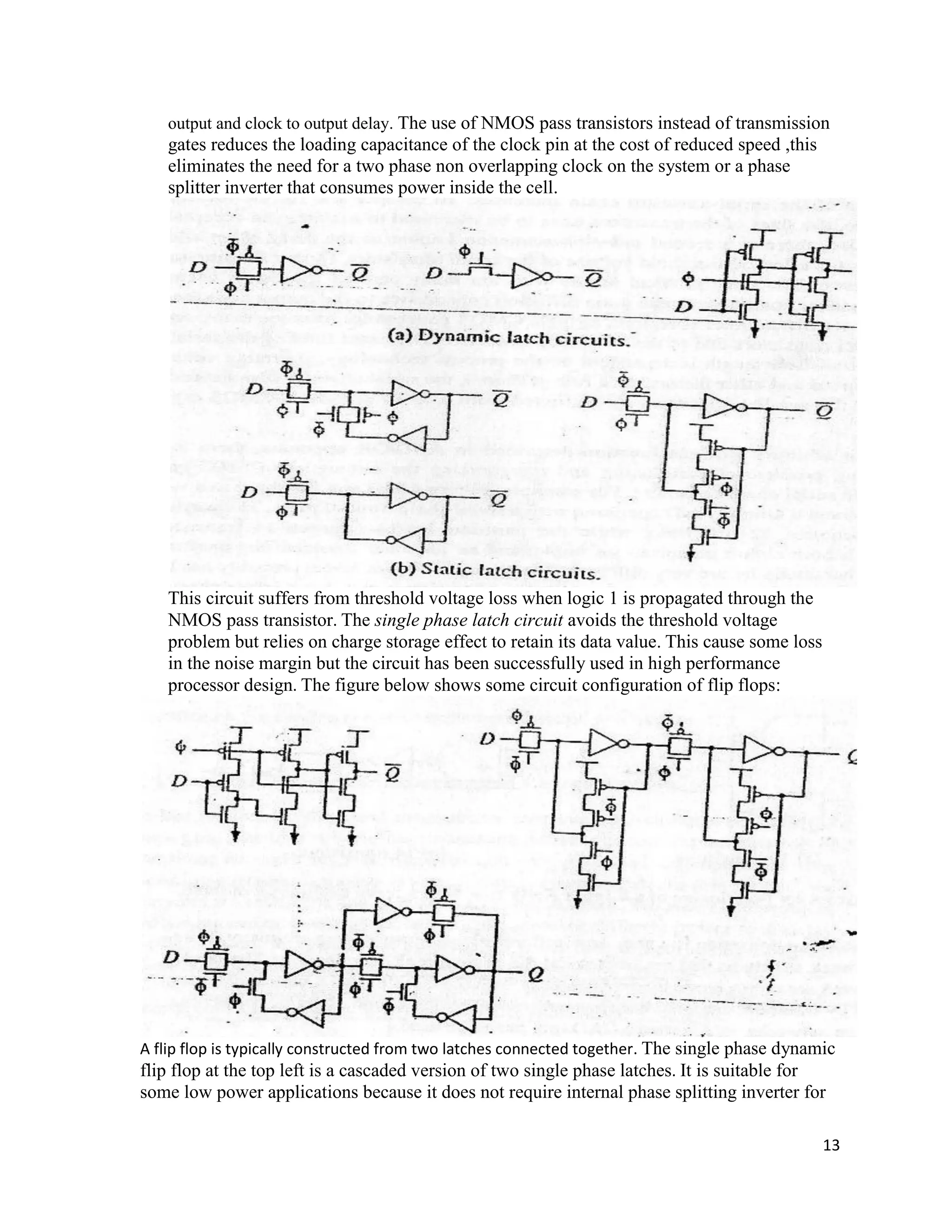
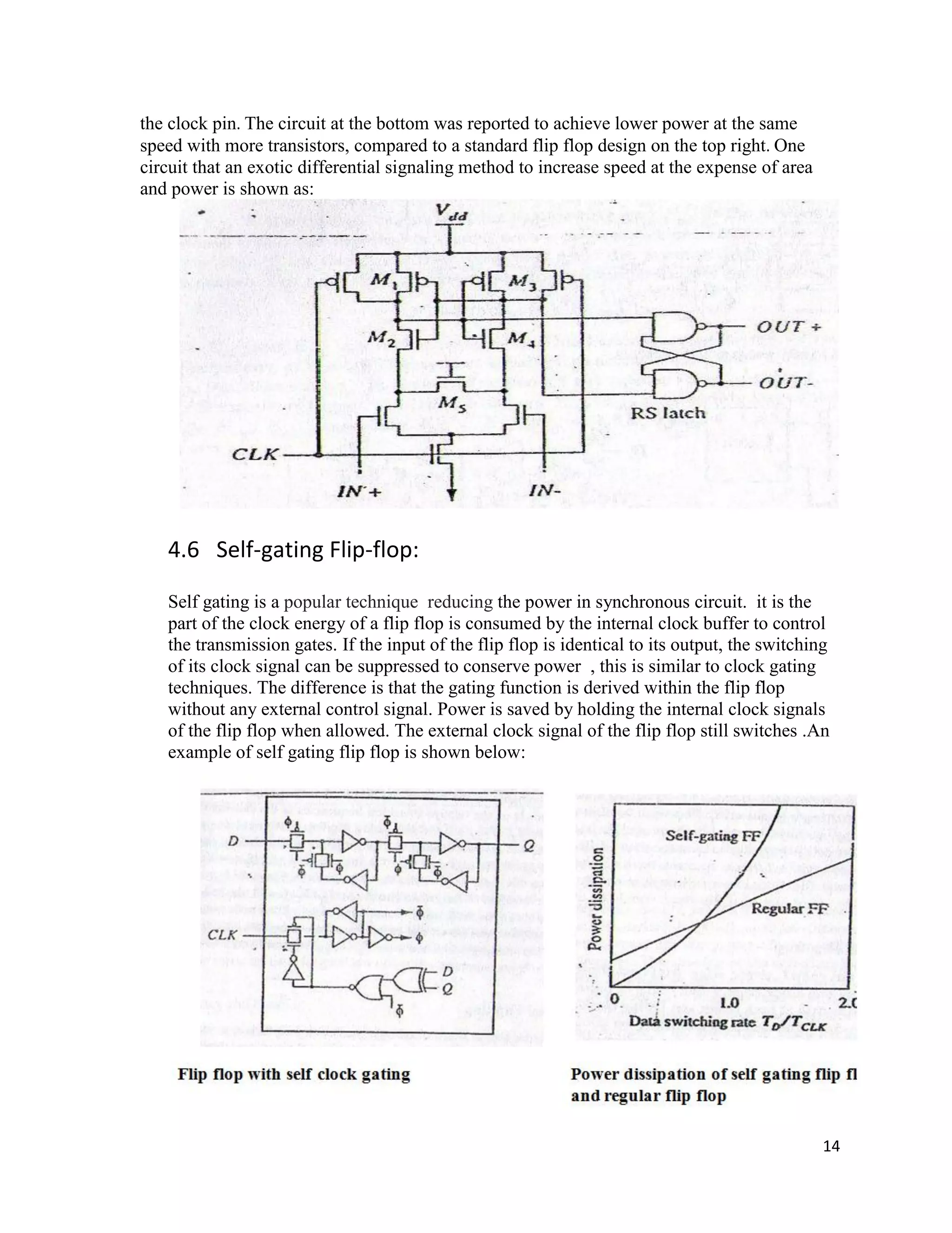
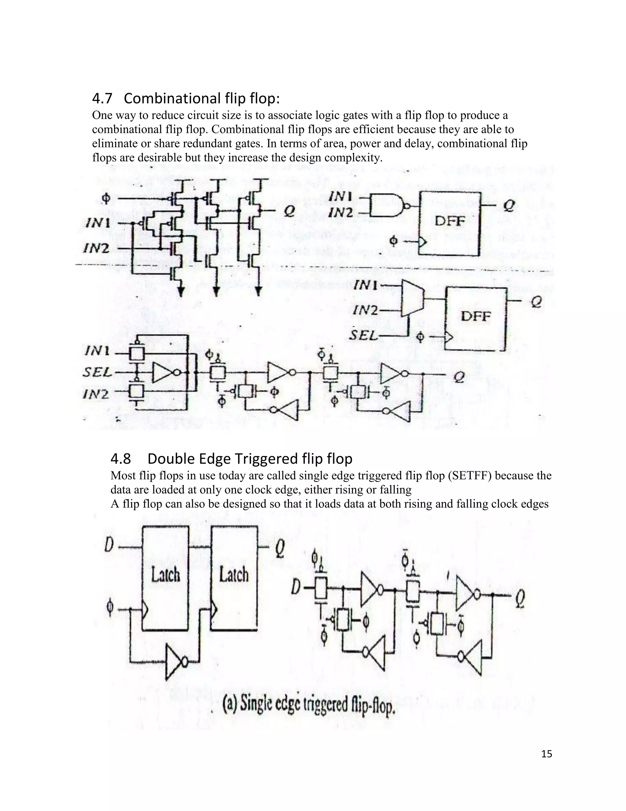
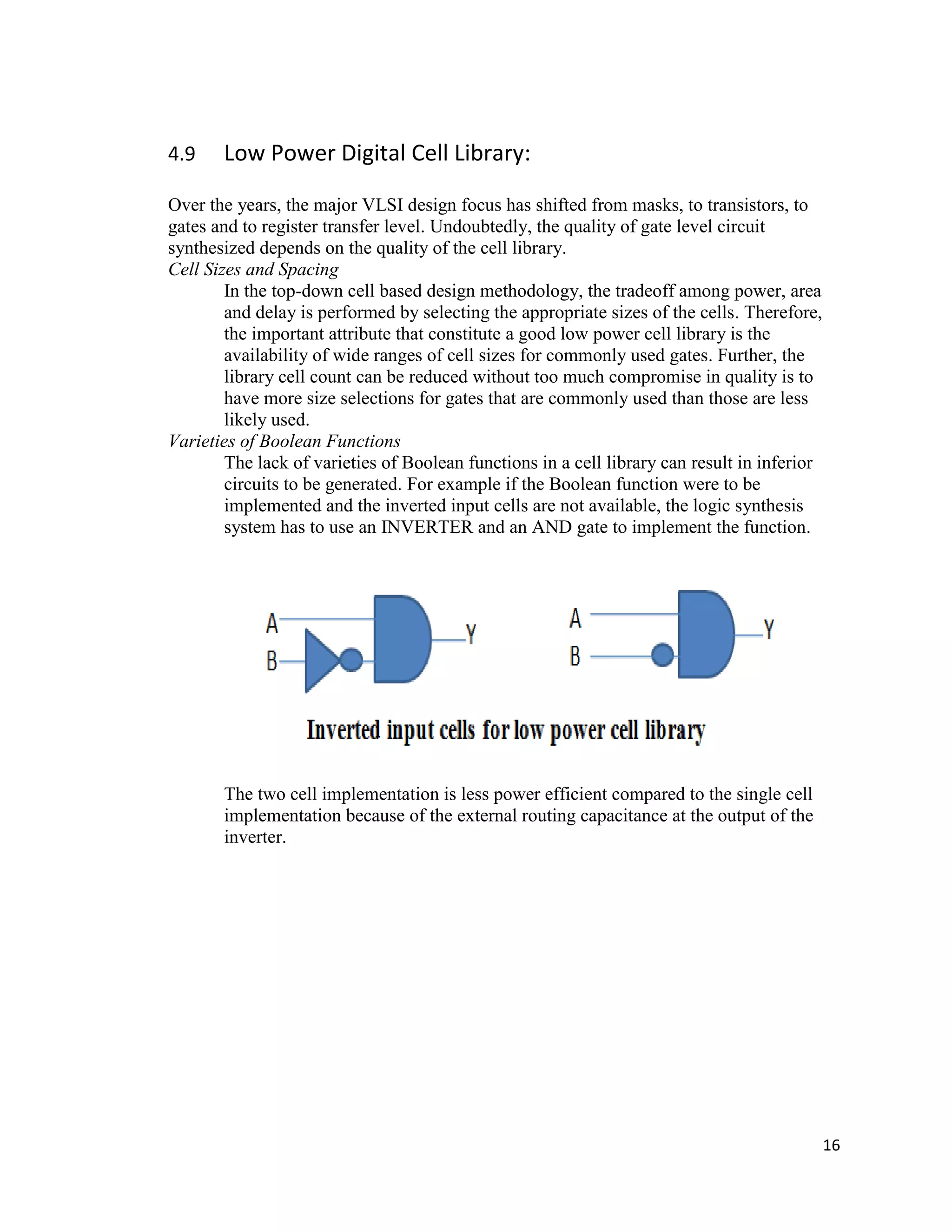
This document discusses sources of power consumption in digital CMOS circuits and techniques for low power VLSI design at the circuit level. It covers the four main sources of power consumption: leakage power, short-circuit power, static power, and switching power. It then discusses various low power design techniques at the circuit level, including transistor and gate sizing, equivalent pin ordering, network restructuring, transistor network partitioning, and low power flip-flop designs. The goal is to optimize power consumption through techniques like minimizing switching activity, reducing capacitive loads, and optimizing transistor sizing.
