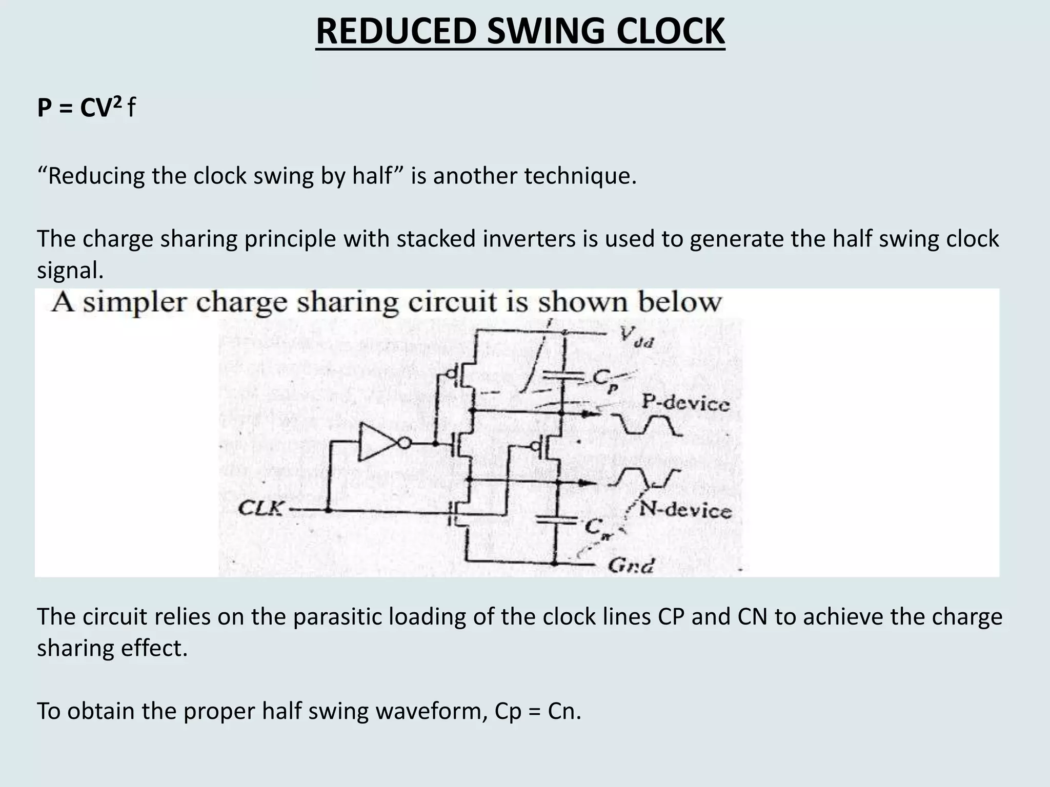
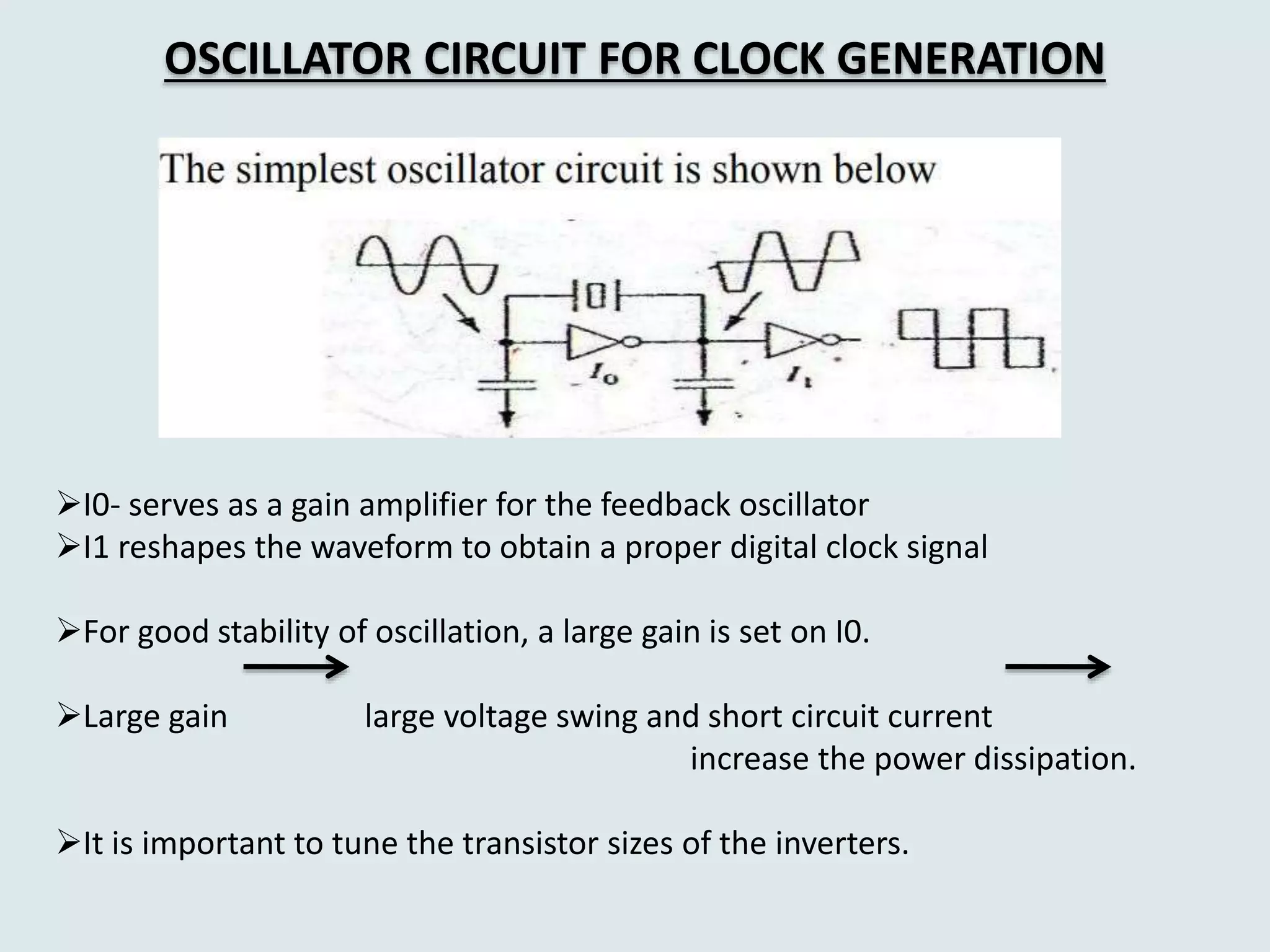
SlideShare a Scribd company logo
Presented by
Shruti Shreya
M. Tech (VLSI)
INTRODUCTION
High Power dissipation leads to
 High efforts for cooling
 Increasing operational costs
 Reduced reliability
 Levels of optimization
System
Algorithm
Architecture
Gate
Transistor
T
T
+
ST1
ALU
MEM
MEM
MP3
Savings Speed Error
> 70 %
40-70 %
25-40 %
15-25 %
10-15 %
Seconds
Minute
Minutes
Hour
Hours
> 50 %
25-50 %
15-30 %
10-20 %
5-10 %
Power reduction in clock networks
In special technique
• More manual effort is required
• Design automation is less efficient in this area.
Clock signal: main source of power dissipation due to high
frequency and load
In a synchronous digital chip, the clock signal is generally one
with the highest frequency.
Clock distribution can take up to 40% of the total power
dissipation of a high performance microprocessor
CLOCK GATING
Technique for power reduction of clock signals
Clock gating saves power by reducing unnecessary clock activities
inside the gated module.
Usually, NAND or NOR gate is used in this process.
It is the process of mask the unwanted signal from propagation forward.
Gating signal should be enabled or disabled at a much slower rate compared
to the clock frequency.
REDUCED SWING CLOCK
P = CV2 f
“Reducing the clock swing by half” is another technique.
The charge sharing principle with stacked inverters is used to generate the half swing clock
signal.
The circuit relies on the parasitic loading of the clock lines CP and CN to achieve the charge
sharing effect.
To obtain the proper half swing waveform, Cp = Cn.
OSCILLATOR CIRCUIT FOR CLOCK GENERATION
I0- serves as a gain amplifier for the feedback oscillator
I1 reshapes the waveform to obtain a proper digital clock signal
For good stability of oscillation, a large gain is set on I0.
Large gain large voltage swing and short circuit current
increase the power dissipation.
It is important to tune the transistor sizes of the inverters.
CMOS FLOATING NODE
Floating nodes are
 internal nodes of a circuit that
 not driven to a logic 0 or logic 1
They should always be avoided
causes overheating and permanently failure of circuit.
Example:
If signals SEL_A and SEL_B are both not asserted, signal OUT will float to an
unknown level.
Downstream logic may interpret OUT as a logic 1 or a logic 0.
REDUCTION OF CMOS FLOATING NODE
Tristate Keeper Circuit
• Applicable when a chip enters in sleep mode or partial
power down mode and busses are not in used.
Blocking Gate
 NAND is used as blocking gate
 It requires a control signal for proper operation.
 This technique is also useful in blocking unwanted signal
transitions, thus saving power.
Special technique in Low Power VLSI design

More Related Content

What's hot

FPGA
FPGAFPGA
LOW POWER DESIGN VLSI
LOW POWER DESIGN VLSILOW POWER DESIGN VLSI
LOW POWER DESIGN VLSI
Duronto riyad
 
Asic design
Asic designAsic design
Power dissipation cmos
Power dissipation cmosPower dissipation cmos
Power dissipation cmos
Rajesh Tiwary
 
Low power VLSI design
Low power VLSI designLow power VLSI design
Low power VLSI design
Saravanan Siddhan
 
fpga programming
fpga programmingfpga programming
fpga programmingAnish Gupta
 
faults in digital systems
faults in digital systemsfaults in digital systems
faults in digital systems
dennis gookyi
 
Clock Gating
Clock GatingClock Gating
Clock Gating
Mahesh Dananjaya
 
Pass Transistor Logic
Pass Transistor LogicPass Transistor Logic
Pass Transistor LogicDiwaker Pant
 
Vlsi power estimation
Vlsi power estimationVlsi power estimation
Vlsi power estimation
Mahesh Dananjaya
 
Low Power Design Approach in VLSI
Low Power Design Approach in VLSILow Power Design Approach in VLSI
Low Power Design Approach in VLSI
Silicon Mentor
 
Power Gating
Power GatingPower Gating
Power Gating
Mahesh Dananjaya
 
Low Power Techniques
Low Power TechniquesLow Power Techniques
Low Power Techniques
keshava murali
 
EC6601 VLSI Design Memory Circuits
EC6601 VLSI Design   Memory CircuitsEC6601 VLSI Design   Memory Circuits
EC6601 VLSI Design Memory Circuits
chitrarengasamy
 
Finfet Technology
Finfet TechnologyFinfet Technology
Finfet Technology
Srinivas Vasamsetti
 
Low power in vlsi with upf basics part 1
Low power in vlsi with upf basics part 1Low power in vlsi with upf basics part 1
Low power in vlsi with upf basics part 1
SUNODH GARLAPATI
 
MOSFET and Short channel effects
MOSFET and Short channel effectsMOSFET and Short channel effects
MOSFET and Short channel effects
Lee Rather
 
Low Power VLSI Design Presentation_final
Low Power VLSI Design Presentation_finalLow Power VLSI Design Presentation_final
Low Power VLSI Design Presentation_finalJITENDER -
 
VLSI routing
VLSI routingVLSI routing
VLSI routing
Naveen Kumar
 
Layout & Stick Diagram Design Rules
Layout & Stick Diagram Design RulesLayout & Stick Diagram Design Rules
Layout & Stick Diagram Design Rules
varun kumar
 

What's hot (20)

FPGA
FPGAFPGA
FPGA
 
LOW POWER DESIGN VLSI
LOW POWER DESIGN VLSILOW POWER DESIGN VLSI
LOW POWER DESIGN VLSI
 
Asic design
Asic designAsic design
Asic design
 
Power dissipation cmos
Power dissipation cmosPower dissipation cmos
Power dissipation cmos
 
Low power VLSI design
Low power VLSI designLow power VLSI design
Low power VLSI design
 
fpga programming
fpga programmingfpga programming
fpga programming
 
faults in digital systems
faults in digital systemsfaults in digital systems
faults in digital systems
 
Clock Gating
Clock GatingClock Gating
Clock Gating
 
Pass Transistor Logic
Pass Transistor LogicPass Transistor Logic
Pass Transistor Logic
 
Vlsi power estimation
Vlsi power estimationVlsi power estimation
Vlsi power estimation
 
Low Power Design Approach in VLSI
Low Power Design Approach in VLSILow Power Design Approach in VLSI
Low Power Design Approach in VLSI
 
Power Gating
Power GatingPower Gating
Power Gating
 
Low Power Techniques
Low Power TechniquesLow Power Techniques
Low Power Techniques
 
EC6601 VLSI Design Memory Circuits
EC6601 VLSI Design   Memory CircuitsEC6601 VLSI Design   Memory Circuits
EC6601 VLSI Design Memory Circuits
 
Finfet Technology
Finfet TechnologyFinfet Technology
Finfet Technology
 
Low power in vlsi with upf basics part 1
Low power in vlsi with upf basics part 1Low power in vlsi with upf basics part 1
Low power in vlsi with upf basics part 1
 
MOSFET and Short channel effects
MOSFET and Short channel effectsMOSFET and Short channel effects
MOSFET and Short channel effects
 
Low Power VLSI Design Presentation_final
Low Power VLSI Design Presentation_finalLow Power VLSI Design Presentation_final
Low Power VLSI Design Presentation_final
 
VLSI routing
VLSI routingVLSI routing
VLSI routing
 
Layout & Stick Diagram Design Rules
Layout & Stick Diagram Design RulesLayout & Stick Diagram Design Rules
Layout & Stick Diagram Design Rules
 

Similar to Special technique in Low Power VLSI design

INTERRUPT DRIVEN MULTIPLEXED 7 SEGMENT DIGITAL CLOCK
INTERRUPT DRIVEN MULTIPLEXED 7 SEGMENT DIGITAL CLOCKINTERRUPT DRIVEN MULTIPLEXED 7 SEGMENT DIGITAL CLOCK
INTERRUPT DRIVEN MULTIPLEXED 7 SEGMENT DIGITAL CLOCK
Santanu Chatterjee
 
DIGITAL HEART BEAT COUNTER
DIGITAL HEART BEAT COUNTERDIGITAL HEART BEAT COUNTER
DIGITAL HEART BEAT COUNTERDeevanshu Swani
 
Design & implementation of 16 bit low power ALU with clock gating
Design & implementation of 16 bit low power ALU with clock gatingDesign & implementation of 16 bit low power ALU with clock gating
Design & implementation of 16 bit low power ALU with clock gating
IRJET Journal
 
Doc speed control of a dc motor using micro controller 8051
Doc speed control of a dc motor using micro controller 8051Doc speed control of a dc motor using micro controller 8051
Doc speed control of a dc motor using micro controller 8051
embdnew
 
Speed control of D.C motor using Pusle width modulation
Speed control of D.C motor using Pusle width modulationSpeed control of D.C motor using Pusle width modulation
Speed control of D.C motor using Pusle width modulation
SantoshkumarVarry
 
LTC3529: Step-Up DC/DC Converter for USB OTG
LTC3529: Step-Up DC/DC Converter for USB OTGLTC3529: Step-Up DC/DC Converter for USB OTG
LTC3529: Step-Up DC/DC Converter for USB OTG
Premier Farnell
 
L6283 1.3.pdf
L6283 1.3.pdfL6283 1.3.pdf
L6283 1.3.pdf
NorgenQuintero1
 
Ac closed loop
Ac closed loopAc closed loop
Ac closed loop
PROJECTRONICS
 
Digital Alarm Clock (IC-TMS-8560)
Digital Alarm Clock (IC-TMS-8560)Digital Alarm Clock (IC-TMS-8560)
Digital Alarm Clock (IC-TMS-8560)Chintan Patel
 
Controlling of DC Motor using IC 555 Timer
Controlling of DC Motor using IC 555 TimerControlling of DC Motor using IC 555 Timer
Controlling of DC Motor using IC 555 TimerUpendra Chokka
 
329292817-PLC-Training for new person pptx
329292817-PLC-Training for new person pptx329292817-PLC-Training for new person pptx
329292817-PLC-Training for new person pptx
viveksingh2418
 
Lec 8,9,10 (interfacing)
Lec 8,9,10 (interfacing)Lec 8,9,10 (interfacing)
Lec 8,9,10 (interfacing)
Mohamed Atef
 
Speed control of DC motor using pulse width modulation technique
Speed control of DC motor using pulse width modulation technique Speed control of DC motor using pulse width modulation technique
Speed control of DC motor using pulse width modulation technique
Imanul Mazarbhuiya
 
Ac motor closedloo[p
Ac motor closedloo[pAc motor closedloo[p
Ac motor closedloo[p
Prasanna Jethi
 
About Sine Pulse Width Modulation
About Sine Pulse Width Modulation About Sine Pulse Width Modulation
About Sine Pulse Width Modulation
Edgefxkits & Solutions
 
Performance Comparison of Various Clock Gating Techniques
Performance Comparison of Various Clock Gating TechniquesPerformance Comparison of Various Clock Gating Techniques
Performance Comparison of Various Clock Gating Techniques
iosrjce
 
automation slides,plc,scada,HMI
automation slides,plc,scada,HMIautomation slides,plc,scada,HMI
automation slides,plc,scada,HMI
BOSCH
 
Automation.pdf
Automation.pdfAutomation.pdf
Automation.pdf
Robin8015873726
 
Optimization of Digitally Controlled Oscillator with Low Power
Optimization of Digitally Controlled Oscillator with Low PowerOptimization of Digitally Controlled Oscillator with Low Power
Optimization of Digitally Controlled Oscillator with Low Power
iosrjce
 

Similar to Special technique in Low Power VLSI design (20)

INTERRUPT DRIVEN MULTIPLEXED 7 SEGMENT DIGITAL CLOCK
INTERRUPT DRIVEN MULTIPLEXED 7 SEGMENT DIGITAL CLOCKINTERRUPT DRIVEN MULTIPLEXED 7 SEGMENT DIGITAL CLOCK
INTERRUPT DRIVEN MULTIPLEXED 7 SEGMENT DIGITAL CLOCK
 
DIGITAL HEART BEAT COUNTER
DIGITAL HEART BEAT COUNTERDIGITAL HEART BEAT COUNTER
DIGITAL HEART BEAT COUNTER
 
Design & implementation of 16 bit low power ALU with clock gating
Design & implementation of 16 bit low power ALU with clock gatingDesign & implementation of 16 bit low power ALU with clock gating
Design & implementation of 16 bit low power ALU with clock gating
 
Doc speed control of a dc motor using micro controller 8051
Doc speed control of a dc motor using micro controller 8051Doc speed control of a dc motor using micro controller 8051
Doc speed control of a dc motor using micro controller 8051
 
Speed control of D.C motor using Pusle width modulation
Speed control of D.C motor using Pusle width modulationSpeed control of D.C motor using Pusle width modulation
Speed control of D.C motor using Pusle width modulation
 
LTC3529: Step-Up DC/DC Converter for USB OTG
LTC3529: Step-Up DC/DC Converter for USB OTGLTC3529: Step-Up DC/DC Converter for USB OTG
LTC3529: Step-Up DC/DC Converter for USB OTG
 
L6283 1.3.pdf
L6283 1.3.pdfL6283 1.3.pdf
L6283 1.3.pdf
 
Ac closed loop
Ac closed loopAc closed loop
Ac closed loop
 
Digital Alarm Clock (IC-TMS-8560)
Digital Alarm Clock (IC-TMS-8560)Digital Alarm Clock (IC-TMS-8560)
Digital Alarm Clock (IC-TMS-8560)
 
Controlling of DC Motor using IC 555 Timer
Controlling of DC Motor using IC 555 TimerControlling of DC Motor using IC 555 Timer
Controlling of DC Motor using IC 555 Timer
 
329292817-PLC-Training for new person pptx
329292817-PLC-Training for new person pptx329292817-PLC-Training for new person pptx
329292817-PLC-Training for new person pptx
 
Lec 8,9,10 (interfacing)
Lec 8,9,10 (interfacing)Lec 8,9,10 (interfacing)
Lec 8,9,10 (interfacing)
 
Speed control of DC motor using pulse width modulation technique
Speed control of DC motor using pulse width modulation technique Speed control of DC motor using pulse width modulation technique
Speed control of DC motor using pulse width modulation technique
 
Ac motor closedloo[p
Ac motor closedloo[pAc motor closedloo[p
Ac motor closedloo[p
 
About Sine Pulse Width Modulation
About Sine Pulse Width Modulation About Sine Pulse Width Modulation
About Sine Pulse Width Modulation
 
Performance Comparison of Various Clock Gating Techniques
Performance Comparison of Various Clock Gating TechniquesPerformance Comparison of Various Clock Gating Techniques
Performance Comparison of Various Clock Gating Techniques
 
Automatic mall elevator
Automatic mall elevatorAutomatic mall elevator
Automatic mall elevator
 
automation slides,plc,scada,HMI
automation slides,plc,scada,HMIautomation slides,plc,scada,HMI
automation slides,plc,scada,HMI
 
Automation.pdf
Automation.pdfAutomation.pdf
Automation.pdf
 
Optimization of Digitally Controlled Oscillator with Low Power
Optimization of Digitally Controlled Oscillator with Low PowerOptimization of Digitally Controlled Oscillator with Low Power
Optimization of Digitally Controlled Oscillator with Low Power
 

More from shrutishreya14

TIMING ISSUES IN DIGITAL CIRCUITS: SYNCHRONOUS DESIGN
TIMING ISSUES IN DIGITAL CIRCUITS: SYNCHRONOUS DESIGNTIMING ISSUES IN DIGITAL CIRCUITS: SYNCHRONOUS DESIGN
TIMING ISSUES IN DIGITAL CIRCUITS: SYNCHRONOUS DESIGN
shrutishreya14
 
Analog to digital converter
Analog to digital converterAnalog to digital converter
Analog to digital converter
shrutishreya14
 
Mental resilence for happy and healthy life
Mental resilence for happy and healthy lifeMental resilence for happy and healthy life
Mental resilence for happy and healthy life
shrutishreya14
 
Behavioral science ppt
Behavioral science pptBehavioral science ppt
Behavioral science ppt
shrutishreya14
 
Dfg & sg ppt (1)
Dfg & sg ppt (1)Dfg & sg ppt (1)
Dfg & sg ppt (1)
shrutishreya14
 
group dymanics
group dymanicsgroup dymanics
group dymanics
shrutishreya14
 
women's and child right
women's and child rightwomen's and child right
women's and child rightshrutishreya14
 

More from shrutishreya14 (9)

TIMING ISSUES IN DIGITAL CIRCUITS: SYNCHRONOUS DESIGN
TIMING ISSUES IN DIGITAL CIRCUITS: SYNCHRONOUS DESIGNTIMING ISSUES IN DIGITAL CIRCUITS: SYNCHRONOUS DESIGN
TIMING ISSUES IN DIGITAL CIRCUITS: SYNCHRONOUS DESIGN
 
Analog to digital converter
Analog to digital converterAnalog to digital converter
Analog to digital converter
 
Mental resilence for happy and healthy life
Mental resilence for happy and healthy lifeMental resilence for happy and healthy life
Mental resilence for happy and healthy life
 
Behavioral science ppt
Behavioral science pptBehavioral science ppt
Behavioral science ppt
 
Dfg & sg ppt (1)
Dfg & sg ppt (1)Dfg & sg ppt (1)
Dfg & sg ppt (1)
 
group dymanics
group dymanicsgroup dymanics
group dymanics
 
Presentation1
Presentation1Presentation1
Presentation1
 
women's and child right
women's and child rightwomen's and child right
women's and child right
 
presentation skilll
presentation skilllpresentation skilll
presentation skilll
 

Recently uploaded

DESIGN A COTTON SEED SEPARATION MACHINE.docx
DESIGN A COTTON SEED SEPARATION MACHINE.docxDESIGN A COTTON SEED SEPARATION MACHINE.docx
DESIGN A COTTON SEED SEPARATION MACHINE.docx
FluxPrime1
 
Railway Signalling Principles Edition 3.pdf
Railway Signalling Principles Edition 3.pdfRailway Signalling Principles Edition 3.pdf
Railway Signalling Principles Edition 3.pdf
TeeVichai
 
CFD Simulation of By-pass Flow in a HRSG module by R&R Consult.pptx
CFD Simulation of By-pass Flow in a HRSG module by R&R Consult.pptxCFD Simulation of By-pass Flow in a HRSG module by R&R Consult.pptx
CFD Simulation of By-pass Flow in a HRSG module by R&R Consult.pptx
R&R Consult
 
Standard Reomte Control Interface - Neometrix
Standard Reomte Control Interface - NeometrixStandard Reomte Control Interface - Neometrix
Standard Reomte Control Interface - Neometrix
Neometrix_Engineering_Pvt_Ltd
 
NO1 Uk best vashikaran specialist in delhi vashikaran baba near me online vas...
NO1 Uk best vashikaran specialist in delhi vashikaran baba near me online vas...NO1 Uk best vashikaran specialist in delhi vashikaran baba near me online vas...
NO1 Uk best vashikaran specialist in delhi vashikaran baba near me online vas...
Amil Baba Dawood bangali
 
Nuclear Power Economics and Structuring 2024
Nuclear Power Economics and Structuring 2024Nuclear Power Economics and Structuring 2024
Nuclear Power Economics and Structuring 2024
Massimo Talia
 
ASME IX(9) 2007 Full Version .pdf
ASME IX(9)  2007 Full Version       .pdfASME IX(9)  2007 Full Version       .pdf
ASME IX(9) 2007 Full Version .pdf
AhmedHussein950959
 
H.Seo, ICLR 2024, MLILAB, KAIST AI.pdf
H.Seo,  ICLR 2024, MLILAB,  KAIST AI.pdfH.Seo,  ICLR 2024, MLILAB,  KAIST AI.pdf
H.Seo, ICLR 2024, MLILAB, KAIST AI.pdf
MLILAB
 
Student information management system project report ii.pdf
Student information management system project report ii.pdfStudent information management system project report ii.pdf
Student information management system project report ii.pdf
Kamal Acharya
 
Immunizing Image Classifiers Against Localized Adversary Attacks
Immunizing Image Classifiers Against Localized Adversary AttacksImmunizing Image Classifiers Against Localized Adversary Attacks
Immunizing Image Classifiers Against Localized Adversary Attacks
gerogepatton
 
Top 10 Oil and Gas Projects in Saudi Arabia 2024.pdf
Top 10 Oil and Gas Projects in Saudi Arabia 2024.pdfTop 10 Oil and Gas Projects in Saudi Arabia 2024.pdf
Top 10 Oil and Gas Projects in Saudi Arabia 2024.pdf
Teleport Manpower Consultant
 
Architectural Portfolio Sean Lockwood
Architectural Portfolio Sean LockwoodArchitectural Portfolio Sean Lockwood
Architectural Portfolio Sean Lockwood
seandesed
 
Forklift Classes Overview by Intella Parts
Forklift Classes Overview by Intella PartsForklift Classes Overview by Intella Parts
Forklift Classes Overview by Intella Parts
Intella Parts
 
AKS UNIVERSITY Satna Final Year Project By OM Hardaha.pdf
AKS UNIVERSITY Satna Final Year Project By OM Hardaha.pdfAKS UNIVERSITY Satna Final Year Project By OM Hardaha.pdf
AKS UNIVERSITY Satna Final Year Project By OM Hardaha.pdf
SamSarthak3
 
WATER CRISIS and its solutions-pptx 1234
WATER CRISIS and its solutions-pptx 1234WATER CRISIS and its solutions-pptx 1234
WATER CRISIS and its solutions-pptx 1234
AafreenAbuthahir2
 
block diagram and signal flow graph representation
block diagram and signal flow graph representationblock diagram and signal flow graph representation
block diagram and signal flow graph representation
Divya Somashekar
 
weather web application report.pdf
weather web application report.pdfweather web application report.pdf
weather web application report.pdf
Pratik Pawar
 
Gen AI Study Jams _ For the GDSC Leads in India.pdf
Gen AI Study Jams _ For the GDSC Leads in India.pdfGen AI Study Jams _ For the GDSC Leads in India.pdf
Gen AI Study Jams _ For the GDSC Leads in India.pdf
gdsczhcet
 
Event Management System Vb Net Project Report.pdf
Event Management System Vb Net  Project Report.pdfEvent Management System Vb Net  Project Report.pdf
Event Management System Vb Net Project Report.pdf
Kamal Acharya
 
一比一原版(SFU毕业证)西蒙菲莎大学毕业证成绩单如何办理
一比一原版(SFU毕业证)西蒙菲莎大学毕业证成绩单如何办理一比一原版(SFU毕业证)西蒙菲莎大学毕业证成绩单如何办理
一比一原版(SFU毕业证)西蒙菲莎大学毕业证成绩单如何办理
bakpo1
 

Recently uploaded (20)

DESIGN A COTTON SEED SEPARATION MACHINE.docx
DESIGN A COTTON SEED SEPARATION MACHINE.docxDESIGN A COTTON SEED SEPARATION MACHINE.docx
DESIGN A COTTON SEED SEPARATION MACHINE.docx
 
Railway Signalling Principles Edition 3.pdf
Railway Signalling Principles Edition 3.pdfRailway Signalling Principles Edition 3.pdf
Railway Signalling Principles Edition 3.pdf
 
CFD Simulation of By-pass Flow in a HRSG module by R&R Consult.pptx
CFD Simulation of By-pass Flow in a HRSG module by R&R Consult.pptxCFD Simulation of By-pass Flow in a HRSG module by R&R Consult.pptx
CFD Simulation of By-pass Flow in a HRSG module by R&R Consult.pptx
 
Standard Reomte Control Interface - Neometrix
Standard Reomte Control Interface - NeometrixStandard Reomte Control Interface - Neometrix
Standard Reomte Control Interface - Neometrix
 
NO1 Uk best vashikaran specialist in delhi vashikaran baba near me online vas...
NO1 Uk best vashikaran specialist in delhi vashikaran baba near me online vas...NO1 Uk best vashikaran specialist in delhi vashikaran baba near me online vas...
NO1 Uk best vashikaran specialist in delhi vashikaran baba near me online vas...
 
Nuclear Power Economics and Structuring 2024
Nuclear Power Economics and Structuring 2024Nuclear Power Economics and Structuring 2024
Nuclear Power Economics and Structuring 2024
 
ASME IX(9) 2007 Full Version .pdf
ASME IX(9)  2007 Full Version       .pdfASME IX(9)  2007 Full Version       .pdf
ASME IX(9) 2007 Full Version .pdf
 
H.Seo, ICLR 2024, MLILAB, KAIST AI.pdf
H.Seo,  ICLR 2024, MLILAB,  KAIST AI.pdfH.Seo,  ICLR 2024, MLILAB,  KAIST AI.pdf
H.Seo, ICLR 2024, MLILAB, KAIST AI.pdf
 
Student information management system project report ii.pdf
Student information management system project report ii.pdfStudent information management system project report ii.pdf
Student information management system project report ii.pdf
 
Immunizing Image Classifiers Against Localized Adversary Attacks
Immunizing Image Classifiers Against Localized Adversary AttacksImmunizing Image Classifiers Against Localized Adversary Attacks
Immunizing Image Classifiers Against Localized Adversary Attacks
 
Top 10 Oil and Gas Projects in Saudi Arabia 2024.pdf
Top 10 Oil and Gas Projects in Saudi Arabia 2024.pdfTop 10 Oil and Gas Projects in Saudi Arabia 2024.pdf
Top 10 Oil and Gas Projects in Saudi Arabia 2024.pdf
 
Architectural Portfolio Sean Lockwood
Architectural Portfolio Sean LockwoodArchitectural Portfolio Sean Lockwood
Architectural Portfolio Sean Lockwood
 
Forklift Classes Overview by Intella Parts
Forklift Classes Overview by Intella PartsForklift Classes Overview by Intella Parts
Forklift Classes Overview by Intella Parts
 
AKS UNIVERSITY Satna Final Year Project By OM Hardaha.pdf
AKS UNIVERSITY Satna Final Year Project By OM Hardaha.pdfAKS UNIVERSITY Satna Final Year Project By OM Hardaha.pdf
AKS UNIVERSITY Satna Final Year Project By OM Hardaha.pdf
 
WATER CRISIS and its solutions-pptx 1234
WATER CRISIS and its solutions-pptx 1234WATER CRISIS and its solutions-pptx 1234
WATER CRISIS and its solutions-pptx 1234
 
block diagram and signal flow graph representation
block diagram and signal flow graph representationblock diagram and signal flow graph representation
block diagram and signal flow graph representation
 
weather web application report.pdf
weather web application report.pdfweather web application report.pdf
weather web application report.pdf
 
Gen AI Study Jams _ For the GDSC Leads in India.pdf
Gen AI Study Jams _ For the GDSC Leads in India.pdfGen AI Study Jams _ For the GDSC Leads in India.pdf
Gen AI Study Jams _ For the GDSC Leads in India.pdf
 
Event Management System Vb Net Project Report.pdf
Event Management System Vb Net  Project Report.pdfEvent Management System Vb Net  Project Report.pdf
Event Management System Vb Net Project Report.pdf
 
一比一原版(SFU毕业证)西蒙菲莎大学毕业证成绩单如何办理
一比一原版(SFU毕业证)西蒙菲莎大学毕业证成绩单如何办理一比一原版(SFU毕业证)西蒙菲莎大学毕业证成绩单如何办理
一比一原版(SFU毕业证)西蒙菲莎大学毕业证成绩单如何办理
 

Special technique in Low Power VLSI design

  • 2. INTRODUCTION High Power dissipation leads to  High efforts for cooling  Increasing operational costs  Reduced reliability  Levels of optimization System Algorithm Architecture Gate Transistor T T + ST1 ALU MEM MEM MP3 Savings Speed Error > 70 % 40-70 % 25-40 % 15-25 % 10-15 % Seconds Minute Minutes Hour Hours > 50 % 25-50 % 15-30 % 10-20 % 5-10 %
  • 3. Power reduction in clock networks In special technique • More manual effort is required • Design automation is less efficient in this area. Clock signal: main source of power dissipation due to high frequency and load In a synchronous digital chip, the clock signal is generally one with the highest frequency. Clock distribution can take up to 40% of the total power dissipation of a high performance microprocessor
  • 4. CLOCK GATING Technique for power reduction of clock signals Clock gating saves power by reducing unnecessary clock activities inside the gated module. Usually, NAND or NOR gate is used in this process. It is the process of mask the unwanted signal from propagation forward. Gating signal should be enabled or disabled at a much slower rate compared to the clock frequency.
  • 5. REDUCED SWING CLOCK P = CV2 f “Reducing the clock swing by half” is another technique. The charge sharing principle with stacked inverters is used to generate the half swing clock signal. The circuit relies on the parasitic loading of the clock lines CP and CN to achieve the charge sharing effect. To obtain the proper half swing waveform, Cp = Cn.
  • 6. OSCILLATOR CIRCUIT FOR CLOCK GENERATION I0- serves as a gain amplifier for the feedback oscillator I1 reshapes the waveform to obtain a proper digital clock signal For good stability of oscillation, a large gain is set on I0. Large gain large voltage swing and short circuit current increase the power dissipation. It is important to tune the transistor sizes of the inverters.
  • 7. CMOS FLOATING NODE Floating nodes are  internal nodes of a circuit that  not driven to a logic 0 or logic 1 They should always be avoided causes overheating and permanently failure of circuit. Example: If signals SEL_A and SEL_B are both not asserted, signal OUT will float to an unknown level. Downstream logic may interpret OUT as a logic 1 or a logic 0.
  • 8. REDUCTION OF CMOS FLOATING NODE Tristate Keeper Circuit • Applicable when a chip enters in sleep mode or partial power down mode and busses are not in used. Blocking Gate  NAND is used as blocking gate  It requires a control signal for proper operation.  This technique is also useful in blocking unwanted signal transitions, thus saving power.