EE222 High-Speed Low-PowerICs
Spring 2017
Instructor: Sung-Mo “Steve” Kang
Room BE-239
skang@ucsc.edu
(831)502-7052
Acknowledgments- Prof. Eby Friedman of the University of
Rochester and Prof. Yusuf Leblebici of EPFL have provided
Lecture materials.
2.
• 4:00 to5:05 PM, M, W, and F
• Baskin Engineering Bldg. Room 156
Time and Place
3.
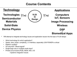
Technology
Technologies
Semiconductor
Materials
Solid-State
Device Physics
Course Contents
Applications
Computers
IoT,Sensors
Image Processing
Wireless
DSP
Biomedical Apps
VLSI
IC
Design
• Will attempt to integrate technology issues and application issues into the topic of VLSI design
• Which technology for which application?
• Speed, area, power, complexity, I/O interface, especially LOW POWER is critical
• Digital or analog?
• On-chip A/D? Mixed-signal?
• Single large chip or multiple small chips?
• Printed circuit board (PCB), MCM, WSI, 3-D
- Systems integration issues
4.
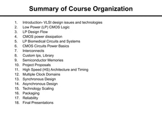
1. Introduction- VLSIdesign issues and technologies
2. Low Power (LP) CMOS Logic
3. LP Design Flow
4. CMOS power dissipation
5. LP Biomedical Circuits and Systems
6. CMOS Circuits Power Basics
7. Interconnects
8. Custom Ips, Library
9. Semiconductor Memories
10. Project Proposals
11. High Speed (HS) Architecture and Timing
12. Multiple Clock Domains
13. Synchronous Design
14. Asynchronous Design
15. Technology Scaling
16. Packaging
17. Reliability
18. Final Presentations
Summary of Course Organization
5.
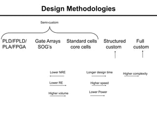
Design Methodologies
PLD/FPLD/ GateArrays Standard cells Structured Full
PLA/FPGA SOG’s core cells custom custom
Higher complexity
Lower Power
Lower NRE Longer design time
Higher speed
Lower RE
Higher volume
Semi-custom
6.
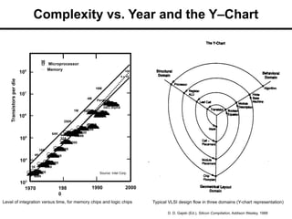
Complexity vs. Yearand the Y–Chart
Typical VLSI design flow in three domains (Y-chart representation)
Level of integration versus time, for memory chips and logic chips
1970 198
0
1990 2000
–
–
–
–
–
–
–
–
–
100
5 x 10⁷
16M
4M
1M
250K
DEC Alpha
80486
Pentium
64K
1K
16K
4K
4004
8008
8085
104
103
105
8048
8080
68000
68030
32A
8066
80386
Bellmac
68020
68040
80286
80860
106
107
108
Microprocessor
Memory
Transistors
per
die
Source: Intel Corp.
D. D. Gajski (Ed.), Silicon Compilation, Addison Wesley, 1988
7.
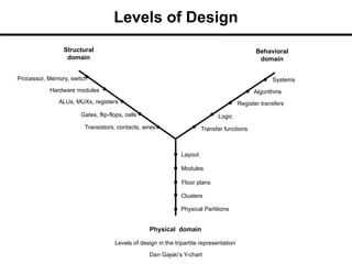
Levels of Design
Levelsof design in the tripartite representation
Dan Gajski’s Y-chart
Processor, Memory, switch
Hardware modules
Transistors, contacts, wires
ALUs, MUXs, registers
Gates, flip-flops, cells
Algorithms
Physical Partitions
Clusters
Modules
Floor plans
Layout
Register transfers
Behavioral
domain
Systems
Logic
Transfer functions
Structural
domain
Physical domain
8.
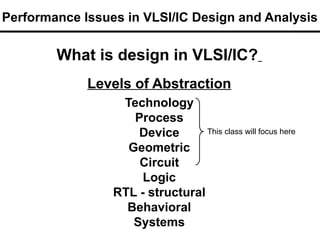
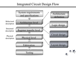
What is designin VLSI/IC?
Levels of Abstraction
Technology
Process
Device
Geometric
Circuit
Logic
RTL - structural
Behavioral
Systems
This class will focus here
Performance Issues in VLSI/IC Design and Analysis
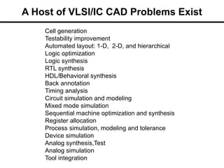
A Host ofVLSI/IC CAD Problems Exist
Cell generation
Testability improvement
Automated layout: 1-D, 2-D, and hierarchical
Logic optimization
Logic synthesis
RTL synthesis
HDL/Behavioral synthesis
Back annotation
Timing analysis
Circuit simulation and modeling
Mixed mode simulation
Sequential machine optimization and synthesis
Register allocation
Process simulation, modeling and tolerance
Device simulation
Analog synthesis,Test
Analog simulation
Tool integration
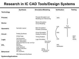
11.
Research in ICCAD Tools/Design Systems
Technology
Process
Device
Geometric
Circuit
Logic
RTL
Behavioral
Systems/Applications
Symbolic Layout
Analog Synthesis
FPGA Tools
Cell Generation
Automated Layout
Logic Optimization
Sequential Machine Opt. and Syn
Module
Generation
Logic Synthesis
Register Allocation
Retiming
RTL Synthesis
HDL Behavioral Synthesis
Process Simulation and
Modeling and Tolerancing
Device Simulation
Circuit Modeling
Back Annotation/
Parasitic Extraction
Circuit Simulation
Analog Simulation
Timing Analysis
Logic Simulation
Verilog
HDL/Behavioral
Simulation
Mixed Mode
Simulation
DRC
LVS
LVS
ERC
BIST
DFT
ATPG
Tool
Integration
HDL
Verification
Synthesis Simulation/Modeling Verification Testing
12.
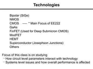
Technologies
Bipolar (SiGe)
NMOS
CMOS *Main Focus of EE222
GaAs
FinFET (Used for Deep Submicron CMOS)
ModFET
HEMT
Superconductor (Josephson Junctions)
Others
Focus of this class is on studying
– How circuit level parameters interact with technology
– Systems level issues and how overall performance is affected
13.
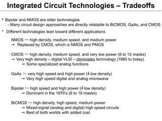
Integrated Circuit Technologies– Tradeoffs
• Bipolar and NMOS are older technologies
- Many circuit design approaches are directly relatable to BiCMOS, GaAs, and CMOS
• Different technologies lean toward different applications
NMOS high density, medium speed, and medium power
→ Replaced by CMOS, which is NMOS and PMOS
CMOS high density, medium speed, and very low power (8 to 12 masks)
→ Very high density – digital VLSI – dominates technology (1985 to today)
→ Some specialized analog functions
GaAs very high speed and high power ( low density)
→ Very high speed digital and analog microwave
Bipolar high speed and high power ( low density)
→ Dominant in the 1970’s (6 to 10 masks)
BiCMOS high density, high speed, medium power
→ Mixed-signal (analog and digital) high speed circuits
→ Best of both worlds with added cost
14.
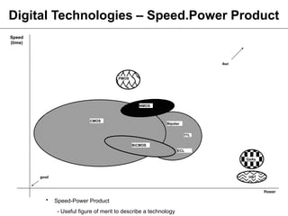
Digital Technologies –Speed.Power Product
• Speed-Power Product
- Useful figure of merit to describe a technology
Speed
(time)
Power
good
PMOS
GaAs
HBT
TTL
Bad
ECL
CMOS
BiCMOS
NMOS
Bipolar
15.
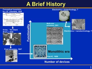
A Brief History
Electronics+ biotechnology, ?
Electronics + nanotechnology, ?
Functionality
Number of devices
First transistor, 1947
First IC, 1959
Multi-core
processor, 2001
Eniac, ``the Giant
Brain,” 1946
Conceptual transistor,
by J.E. Lilienfeld, 1926
Monolithic era
1
16.
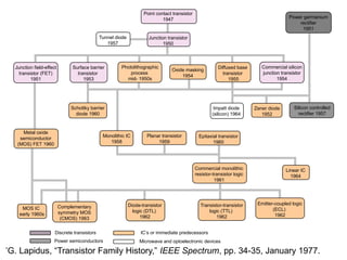
Point contact transistor
1947
Junctiontransistor
1950
Junction field-effect
transistor (FET)
1951
Surface barrier
transistor
1953
Photolithographic
process
mid- 1950s
Oxide masking
1954
Diffused base
transistor
1955
Power germanium
rectifier
1951
Schottky barrier
diode 1960
Impatt diode
(silicon) 1964
Zener diode
1952
Silicon controlled
rectifier 1957
Metal oxide
semiconductor
(MOS) FET 1960
Monolithic IC
1958
Planar transistor
1959
Epitaxial transistor
1960
Commercial monolithic
resistor-transistor logic
1961
MOS IC
early 1960s
Complementary
symmetry MOS
(CMOS) 1963
Diode-transistor
logic (DTL)
1962
Transistor-transistor
logic (TTL)
1962
Emitter-coupled logic
(ECL)
1962
Linear IC
1964
Tunnel diode
1957
Commercial silicon
junction transistor
1954
Discrete transistors
Power semiconductors
IC’s or immediate predecessors
Microwave and optoelectronic devices
*
G. Lapidus, “Transistor Family History,” IEEE Spectrum, pp. 34-35, January 1977.
17.
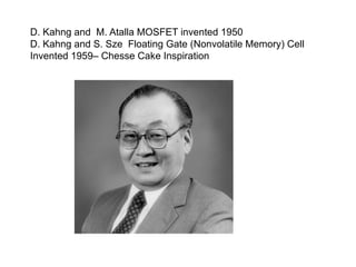
D. Kahng andM. Atalla MOSFET invented 1950
D. Kahng and S. Sze Floating Gate (Nonvolatile Memory) Cell
Invented 1959– Chesse Cake Inspiration
18.
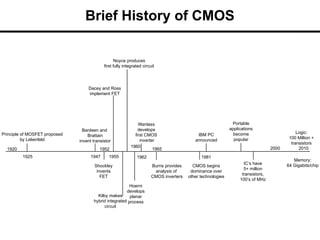
Brief History ofCMOS
1920
1925
Principle of MOSFET proposed
by Lelienfeld
1947
Bardeen and
Brattain
invent transistor
Dacey and Ross
implement FET
Noyce produces
first fully integrated circuit
Shockley
invents
FET
Kilby makes
hybrid integrated
circuit
1955
1952
Hoerni
develops
planar
process
1962
1960
1965
Burns provides
analysis of
CMOS inverters
Wanlass
develops
first CMOS
inverter
CMOS begins
dominance over
other technologies
IBM PC
announced
1981
Portable
applications
become
popular
IC’s have
5+ million
transistors,
100’s of MHz
2000 2010
Memory:
64 Gigabits/chip
Logic:
100 Million +
transistors
19.
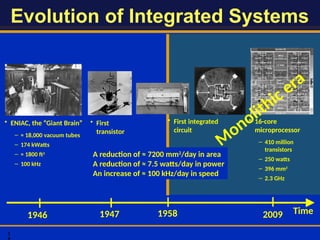
Evolution of IntegratedSystems
Time
2009
1
1946 1947 1958
M
onolithic era
A reduction of ≈ 7200 mm2
/day in area
A reduction of ≈ 7.5 watts/day in power
An increase of ≈ 100 kHz/day in speed
• ENIAC, the “Giant Brain”
– ≈ 18,000 vacuum tubes
– 174 kWatts
– ≈ 1800 ft2
– 100 kHz
• First
transistor
• First integrated
circuit
• 16-core
microprocessor
– 410 million
transistors
– 250 watts
– 396 mm2
– 2.3 GHz
20.
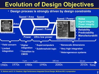
Evolution of DesignObjectives
Area
Power
Speed / Power
Ultra low power
Time
1960s 1980s 1990s 2000s
1970s
5 µm 1 µm 100 nm
2010s
22 nm
Speed / Power / • Noise
Signal integrity
Power integrity
Robustness
• Reliability
• Predictability
• Manufacturabilit
y
Speed / Area Speed
• Yield concern
• Limited
integration
• Higher
integration
• Transition to
CMOS
• Supercomputers
• Subthreshold logic
• Nanoscale dimensions
• Very high integration
• Heterogeneous systems
E. Salman and E. G. Friedman, High Performance Integrated Circuit Design, McGraw-Hill, in preparation
• Design process is strongly driven by design constraints
Infineon, monolithic transceiver
Fairchild Semiconductor
2
21.
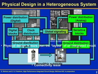
Physical Design ina Heterogeneous System
E. Salman and E. G. Friedman, High Performance Integrated Circuit Design, McGraw-Hill, in preparation
Monolithic substrate
Power distribution
(Digital)
Power distribution
(Analog)
Ground distribution
(Digital)
Ground distribution
(Analog)
Clock
distribution
Digital
blocks
Global signaling
Sensitive
blocks
Monolithic substrate
Infineon, monolithic transceiver
Intel, System-on-Chip, Tolapai
• Physical design is more than the “layout” of an integrated circuit
• Connectivity issue
2
22.
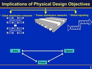
Implications of PhysicalDesign Objectives
Speed
Power
Area
• Global signaling
• Clock distribution networks • Power distribution networks
2
23.
Implications of PhysicalDesign Objectives
• Global signaling
• Clock distribution networks • Power distribution networks
Speed
Power
Area
Signal integrity Power integrity
Robustness
Reliability Manufacturability
Complex tradeoffs
Noise
2
24.
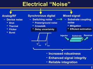
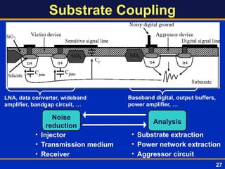
Electrical “Noise”
Analog/RF
– Devicenoise
Shot
Thermal
Flicker
Burst
Synchronous digital
– Switching noise
Power/ground noise
Crosstalk
Delay uncertainty
Mixed-signal
– Substrate coupling
noise
Mitigation
Efficient estimation
T min T max
• Increased robustness
• Enhanced signal integrity
• Reliable integration
Injector Substrate Receiver
2
25.
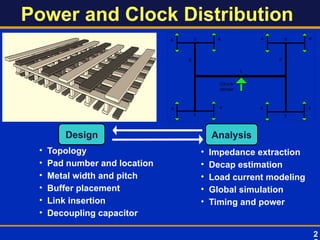
Power and ClockDistribution
• Topology
• Pad number and location
• Metal width and pitch
• Buffer placement
• Link insertion
• Decoupling capacitor
• Impedance extraction
• Decap estimation
• Load current modeling
• Global simulation
• Timing and power
Analysis
Design
Clock
driver
1
2 2
3 3
3 3
4 4 4 4
4 4 4 4
2
26.
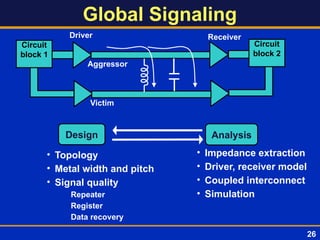
Global Signaling
Circuit
block 1
•Topology
• Metal width and pitch
• Signal quality
Repeater
Register
Data recovery
• Impedance extraction
• Driver, receiver model
• Coupled interconnect
• Simulation
Driver Receiver
Analysis
Design
26
Circuit
block 2
Aggressor
Victim
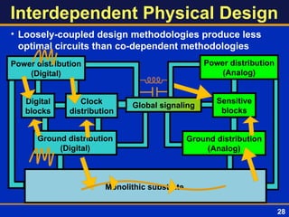
Interdependent Physical Design
•Loosely-coupled design methodologies produce less
optimal circuits than co-dependent methodologies
Monolithic substrate
Power distribution
(Digital)
Power distribution
(Analog)
Ground distribution
(Digital)
Ground distribution
(Analog)
Clock
distribution
Digital
blocks
Global signaling
Sensitive
blocks
Monolithic substrate
28
29.
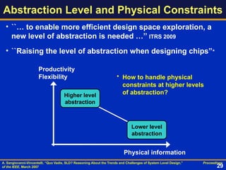
Abstraction Level andPhysical Constraints
• ``… to enable more efficient design space exploration, a
new level of abstraction is needed …’’ ITRS 2009
• ``Raising the level of abstraction when designing chips”*
A. Sangiovanni-Vincentelli, “Quo Vadis, SLD? Reasoning About the Trends and Challenges of System Level Design,” Proceedings
of the IEEE, March 2007
Physical information
Productivity
Flexibility • How to handle physical
constraints at higher levels
of abstraction?
Higher level
abstraction
Lower level
abstraction
29
30.
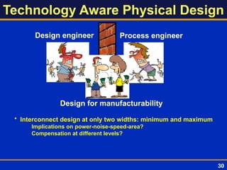
Technology Aware PhysicalDesign
Design engineer Process engineer
Design for manufacturability
• Interconnect design at only two widths: minimum and maximum
Implications on power-noise-speed-area?
Compensation at different levels?
30
31.
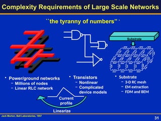
Complexity Requirements ofLarge Scale Networks
• Power/ground networks
− Millions of nodes
− Linear RLC network
• Transistors
− Nonlinear
− Complicated
device models
• Substrate
− 3-D RC mesh
− EM extraction
− FDM and BEM
Current
profile
Substrate
Linearize
``the tyranny of numbers’’ *
Jack Morton, Bell Laboratories, 1957
31
32.
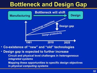
Bottleneck and DesignGap
• Co-existence of “new” and “old” technologies
• Design gap is expected to further increase
Circuit and physical level challenges in heterogeneous
integrated systems
Mapping these opportunities to specific design objectives
in physical computing systems
Design
Manufacturing
Bottleneck will shift
Design gap
1981 2010 2025
Design productivity
Technology capabilities
32
33.
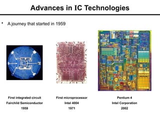
Advances in ICTechnologies
• A journey that started in 1959
First integrated circuit
Fairchild Semiconductor
1959
First microprocessor
Intel 4004
1971
Pentium 4
Intel Corporation
2002
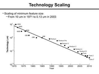
Technology Scaling
– Scalingof minimum feature size
–From 10 um in 1971 to 0.13 um in 2003
4004
i386
8086
Pentium Pro
8080
Pentium
i286
i486
8085
Pentium 4
Pentium 2
Pentium 3
Core
Pentium D
Core 2
Core i7
38.
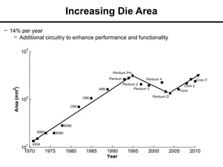
Increasing Die Area
–14% per year
– Additional circuitry to enhance performance and functionality
4004
i386
8086
Pentium Pro
8080
Pentium
i286
i486
8085
Pentium 4
Pentium 2
Pentium 3
Core
Pentium D
Core 2
Core i7
39.
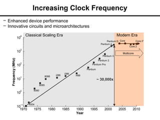
Increasing Clock Frequency
–Enhanced device performance
– Innovative circuits and microarchitectures
~ 30,000x
Classical Scaling Era Modern Era
Multicore
4004
i386
8086
Pentium Pro
8080
Pentium
i286 i486
8085
Pentium 4
Pentium 2
Pentium 3
Core
Pentium D
Core 2
Core i7
40.
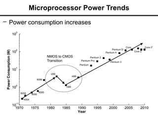
Microprocessor Power Trends
–Power consumption increases
NMOS to CMOS
Transition
4004
i386
8086
Pentium Pro
8080
Pentium
i286
i486
8085
Pentium 4
Pentium 2
Pentium 3
Core
Pentium D
Core 2
Core i7
8008
41.
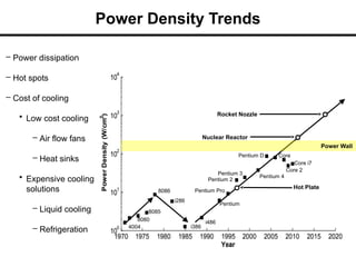
– Power dissipation
–Hot spots
– Cost of cooling
• Low cost cooling
– Air flow fans
– Heat sinks
• Expensive cooling
solutions
– Liquid cooling
– Refrigeration
Power Density Trends
Hot Plate
Nuclear Reactor
Rocket Nozzle
4004 i386
8086 Pentium Pro
8080
Pentium
i286
i486
8085
Pentium 4
Pentium 2
Pentium 3
Core
Pentium D
Core 2
Core i7
Power Wall
42.
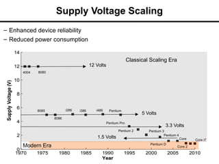
Supply Voltage Scaling
–Enhanced device reliability
– Reduced power consumption
Classical Scaling Era
Modern Era
12 Volts
5 Volts
3.3 Volts
1.5 Volts
4004
i386
8086
Pentium Pro
8080
Pentium
i286 i486
8085
Pentium 4
Pentium 2 Pentium 3
Core
Pentium D
Core 2
Core i7
43.
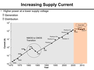
Increasing Supply Current
–Higher power at a lower supply voltage
Generation
Distribution
NMOS to CMOS
Transition
Power Wall
4004
i386
8086
Pentium Pro
8080
Pentium
i286
i486
8085
Pentium 4
Pentium 2 Pentium 3
Core
Pentium D
Core 2
Core i7
44.
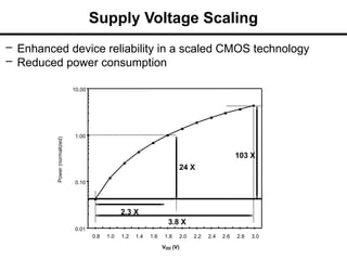
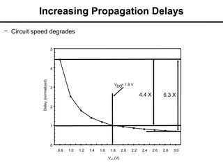
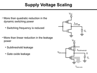
Supply Voltage Scaling
–Enhanced device reliability in a scaled CMOS technology
– Reduced power consumption
0.01
0.10
1.00
10.00
0.8 1.0 1.2 1.4 1.6 1.8 2.0 2.2 2.4 2.6 2.8 3.0
VDD (V)
Power
(normalized)
103 X
24 X
3.8 X
2.3 X
Supply Voltage Scaling
–Morethan quadratic reduction in the
dynamic switching power
• Switching frequency is reduced
–More than linear reduction in the leakage
power
• Subthreshold leakage
• Gate oxide leakage
VDD 0
IGate-oxide
VDD
CL
ISubthreshold
VDD
CL
ILoad
47.
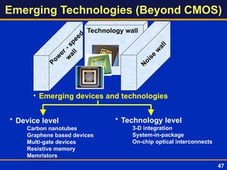
• Emerging devicesand technologies
• Device level
Carbon nanotubes
Graphene based devices
Multi-gate devices
Resistive memory
Memristors
Emerging Technologies (Beyond CMOS)
• Technology level
3-D integration
System-in-package
On-chip optical interconnects
P
o
w
e
r
-
s
p
e
e
d
w
a
l
l
Technology wall
N
o
i
s
e
w
a
l
l 47
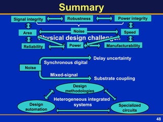
48.
Physical design challenges
Summary
Speed
Power
Area
Signalintegrity Power integrity
Robustness
Reliability Manufacturability
Design
automation
Design
methodologies
Specialized
circuits
Heterogeneous integrated
systems
48
Noise
Synchronous digital
Mixed-signal
Delay uncertainty
Substrate coupling
Noise
49.
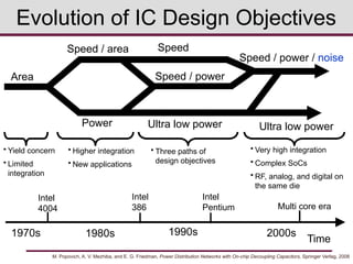
Evolution of ICDesign Objectives
Area
Time
1970s 1980s 1990s 2000s
Speed / area
Power Ultra low power
Speed
Speed / power
Speed / power / noise
Ultra low power
M. Popovich, A. V. Mezhiba, and E. G. Friedman, Power Distribution Networks with On-chip Decoupling Capacitors, Springer Verlag, 2008
• Yield concern
• Limited
integration
Intel
4004
Intel
386
• Higher integration
• New applications
Intel
Pentium
• Three paths of
design objectives
• Very high integration
• Complex SoCs
• RF, analog, and digital on
the same die
Multi core era
50.
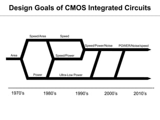
Design Goals ofCMOS Integrated Circuits
2000’s
Speed/Power/Noise
1970’s
Area
1980’s
Speed/Area
Power Ultra-Low Power
Speed
1990’s
Speed/Power
2010’s
POWER/Noise/speed
51.
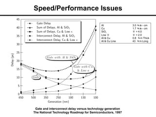
Speed/Performance Issues
Al 3.0 - cm
Cu 1.7 - cm
SiO2 = 4.0
Low = 2.0
Al & Cu 0.8 m Thick
Al & Cu Line 43 m Long
Gate and interconnect delay versus technology generation
The National Technology Roadmap for Semiconductors, 1997
52.
Evolution of ICDesign Objectives
Time
1960s 1980s 1990s 2000s
M. Popovich, A. V. Mezhiba, and E. G. Friedman, Power Distribution Networks with On-Chip Decoupling Capacitors, Springer Verlag, 2008
1970s
1959
2008
Area
Speed / area
Power
Speed
Speed / Power
Ultra low power
4 µm 0.8 µm 0.1 µm
2010s
0.045 µm
• Yield concern
• Limited
integration
• Higher integration
• New applications
• Transition to CMOS
• Supercomputers
• Subthreshold logic
• Very high integration
• Complex SoCs
• RF, analog, and digital
on the same die
Speed / Power / Noise
5
Editor's Notes
#15 Lilienfeld, Max Planc’s student. It had to take another two decades. In the mean time, we had to deal with vacuum tube based computing.
#19 Fairchild IC: 4 transistors, one metal layer
Infineon IC: SiP for GSM/EDGE
60s, metal to polycrystalline and self aligned process (http://www.computerhistory.org/semiconductor/timeline/1968-SGT.html)
1963, cmos invented, but not adopted due to performance limit. (http://www.computerhistory.org/semiconductor/timeline/1963-CMOS.html)
Sub threshold mode logic
Dynamic logic
#20 EMPHASIS HERE NOISE, AND GO TO HETEROG. SYSTEMS TO MOTIVATE NOISE Important to put the design process into perspective. Starts to behave like pure analog circuits where any two parameters trade with each other. Not surprisingly, the design time has increased. Design productivity.
#21 The device is smaller, much more reliable, but the connectivity problem is still there. That’s one of the most fundamental issues in the physical design, also referred to as interconnect problem. Depending upon our research focus, we see different aspects of these circuits. Assuming it is a synchronous system.
#24 The perception of noise is quite different depending upon the type of circuit. In digital synchronous circuits, when we say noise, we primarily refer to switching noise. In mixed-signal circuits, where we have both digital and analog/RF circuits, coupling from digital to analog/RF becomes crictical. Mixed-signal circuits, 66% of the market today. Since switching noise is one of the primary constraints for physical design, I would like to give some more general background on physical design, and then come back to these problems.
#25 Traditionally area and electromigration, now noise and impedance
#26 Larger die area, higher transmission rates, signal integrity. To transfer signal from one signal block to another. Can be on-chip or off-chip. Traditionally, power, speed, still important, but now also noise, noise coupling.
#27 Mixed-signal circuits, if we exclude the pure memory circuits, it is 66% of the semiconductor market is mixed-signal circuits. The nature of the problem has changed.
#28 Refer to physical design conference. I have already shown how interdependence helps in reducing delay uncertainty. Make sure to continue publishing and pushing papers out. Natural extension of my work. We can improve not only signal integrity but also the performance of the circuit or reduce power dissipation. I have showed an example how considering the interdependence in timing constraints reduced pessimism and delay uncertainty with a more robust circuit. Here is another example of considering codependence.
#29 Trend for a higher abstraction level to handle complexity and increase productivity. I am not going to develop that abstraction level, but from my perspective, there is an issue here.
#30 There is always this tension between a design engineer and process engineer, although they don’t typically see each other, design engineer wants more relaxed rules, but the process engineer says you cannot do that. Maybe not this bad, but there is definitely a tension. And especially with the manufacturability being a primary design objective. How can we make physical design more technology aware.
#32 As these technologies and devices get more mature, the bottleneck shifts from manufacturing to design, and we cannot wait to develop design methodologies and circuit challenges until it matures.
#47 From my perspective, the circuit and physical level challenges of these emerging devices and technologies is important. Scaling is expected to continue for another decade, but there are also emerging devices and techs. I will be interested in the circuit and physical level challenges of these new devices and technologies. of the Benefits of scaling is likely to end. Alternative opportunities. Gap further increases with the introduction of 3D, SiP, and other emerging opportunities…
Mention some 3d physical design challenges
#48 I summarized some of the challenges in the physical design, especially with the emergence of new design constraints. I presented some of our research results related to increasing the robustness and efficiently estimating substrate coupling noise which is important for improving signal integrity. Finally, I proposed a framework for future research which has three domains. 1, 2, and 3, for heterogeneous embedded systems.
#49 Advances in the fabrication technology 2) emergence of new applications
60s and 70s: Yield concern is the primary limitation to integration density. Therefore, circuit compactness and area were the primary design objectives. Due to limited integration density, a typical system was composed of many small integrated circuits where the performance was limited by the inter-chip communication.
Due to the advances in the fabrication technology, system speed became a stronger function of the single ICs. Therefore, in 80s,
Speed gained a very high priority as a design objective. At the same time, a new set of applications emerged where power also became very important. These applications include digital wrist watches, handheld calculators, and some satellite electronics.
Later in 90s, with even higher integration, speed and power had to be considered at the same time, resulting in three different paths of design objectives. Ultralow power where speed is not important. Very high speed applications where power is tolerated and those applications where speed and power are optimized at the same time.
Starting 2000, the primary trend was to integrate different functions on the same die such as analog, RF, and digital to reduce the overall cost. A new design metric emerged which was noise.
#52 Fairchild IC: 4 transistors, one metal layer
Infineon IC: SiP for GSM/EDGE
60s, metal to polycrystalline and self aligned process (http://www.computerhistory.org/semiconductor/timeline/1968-SGT.html)
1963, cmos invented, but not adopted due to performance limit. (http://www.computerhistory.org/semiconductor/timeline/1963-CMOS.html)
Sub threshold mode logic
Dynamic logic