IJSRD - International Journal for Scientific Research & Development| Vol. 1, Issue 2, 2013 | ISSN (online): 2321-0613
All rights reserved by www.ijsrd.com 238
Low Power Design flow using Power Format
1
Jinal Patel 2
Ekta Chotai 3
Naincy Desai 4
Hemang Patel
1,2,3
Department of Electronics Engineering, GTU, Ahmedabad, Gujarat, India
4
Department of Electronics Engineering, State Technological University of Madhya Pradesh, Bhopal
(M.P.), India
Abstract— The demand for portable electronic devices that
offers increase in functions, performance at lower costs and
smaller sizes increased rapidly. Designing complex SOCs is
a challenge, especially at 90 nanometers Technology, where
new problems crop up – power efficiency is being the
biggest of problems. For different modes we cannot design
different operating circuits, better to have technique that will
have minimum circuit changes and in all modes it will save
power which is wasted. This paper provides some guidelines
on how Low Power design using UPF approach can be
introduced for a design.
I. INTRODUCTION
The increasing demand for high-performance, battery-
operated, SOC in communication and computing has shifted
the focus from traditional constraints (such as area,
performance, cost, and reliability) to power consumption.
The goal is to reduce on-chip power dissipation to reduce
temperature and minimize cooling requirements, or to
provide longer battery life to mobile and handheld devices.
For instance, as more transistors are integrated onto a single
chip, the power density increases rapidly. Similarly, though
a higher voltage supply can make devices work faster, this
approach is not followed, as the power consumption also
increases with heat–sink components. These factors, in turn,
reduced the limited battery life. Therefore, balancing both
power and performance has become a critical design
requirement.
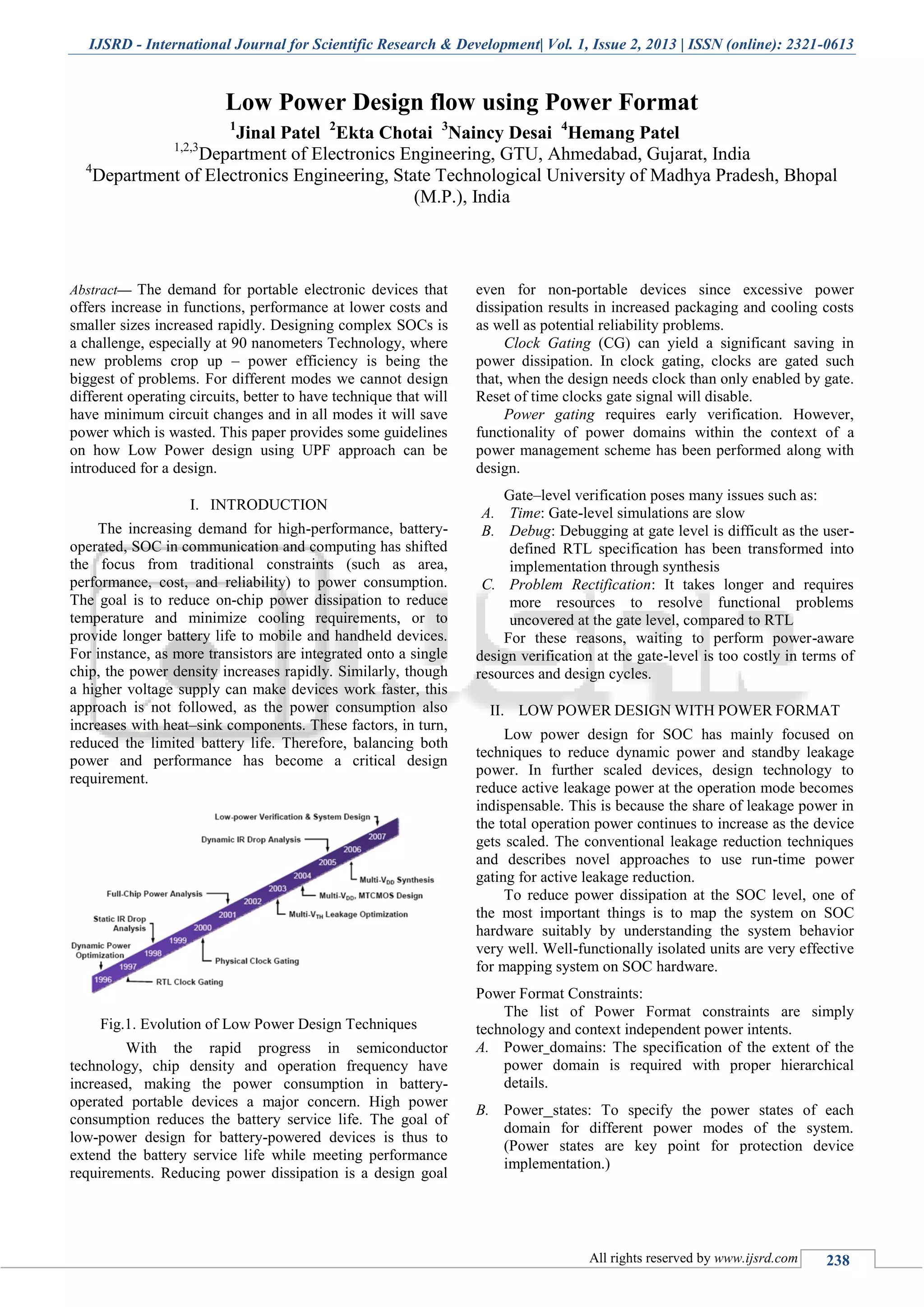
Fig.1. Evolution of Low Power Design Techniques
With the rapid progress in semiconductor
technology, chip density and operation frequency have
increased, making the power consumption in battery-
operated portable devices a major concern. High power
consumption reduces the battery service life. The goal of
low-power design for battery-powered devices is thus to
extend the battery service life while meeting performance
requirements. Reducing power dissipation is a design goal
even for non-portable devices since excessive power
dissipation results in increased packaging and cooling costs
as well as potential reliability problems.
Clock Gating (CG) can yield a significant saving in
power dissipation. In clock gating, clocks are gated such
that, when the design needs clock than only enabled by gate.
Reset of time clocks gate signal will disable.
Power gating requires early verification. However,
functionality of power domains within the context of a
power management scheme has been performed along with
design.
Gate–level verification poses many issues such as:
A. Time: Gate-level simulations are slow
B. Debug: Debugging at gate level is difficult as the user-
defined RTL specification has been transformed into
implementation through synthesis
C. Problem Rectification: It takes longer and requires
more resources to resolve functional problems
uncovered at the gate level, compared to RTL
For these reasons, waiting to perform power-aware
design verification at the gate-level is too costly in terms of
resources and design cycles.
II. LOW POWER DESIGN WITH POWER FORMAT
Low power design for SOC has mainly focused on
techniques to reduce dynamic power and standby leakage
power. In further scaled devices, design technology to
reduce active leakage power at the operation mode becomes
indispensable. This is because the share of leakage power in
the total operation power continues to increase as the device
gets scaled. The conventional leakage reduction techniques
and describes novel approaches to use run-time power
gating for active leakage reduction.
To reduce power dissipation at the SOC level, one of
the most important things is to map the system on SOC
hardware suitably by understanding the system behavior
very well. Well-functionally isolated units are very effective
for mapping system on SOC hardware.
Power Format Constraints:
The list of Power Format constraints are simply
technology and context independent power intents.
A. Power domains: The specification of the extent of the
power domain is required with proper hierarchical
details.
B. Power states: To specify the power states of each
domain for different power modes of the system.
(Power states are key point for protection device
implementation.)
Low power Design Flow Using Power Format
(IJSRD/Vol. 1/Issue 2/2013/0046)
All rights reserved by www.ijsrd.com
239
C. Retention elements: These are simply a list of registers
that require state retention functionality when their
parent domain is switched off.
D. Isolation values: The constraints simply indicate that
when drivers of these inputs are switched off (in the
context where the soft IP is instantiated), the specified
isolation value must be seen at those inputs.
Low Power Design implementation flow for a SOC with
Power Format:
 Section 1: Define power domains.
In this section, the power domains are defined. Power
domain definition is optional except for the top level cell.
This power domain is required to specify the system power
states or some other power intents such as the
Isolation/Level shifter/Retention/Power switch logic.
 Section 2: Define data port, net and interface supply set
handle associations.
Every boundary port is connected to some logic
internally, needs to be associated with one of the interface
supply handle of the power model. This power intent
enables the specification of other power intents, such as
using -source/-sink to filter out ports to be isolated.
The supply ports connected to the external supply nets
must be declared before the physical implementation.
Internal supply ports, such as the output supply port of a
power switch, do not need to be specified.
When we are using UPF’’ after physical
implementation, for the regular logic cells of a power
domain, the power pin and ground pin of each cell are
connected to the primary power net and ground net of the
power domain respectively.
 Section 3: Associate the interfaces of power model to
boundary supply ports or internally generated supplies.
All supply set handles or supply sets created in previous
stages must be resolved with actual supply net definition at
this stage. New supply set needs to be created with the
supply nets and associate the supply set to the previously
declared supply set handle.
 Section 4: Define power states for interface supply
set/port handles.
How to define the power states for each interface
supply set handles of the power model is illustrated. These
states will be used to define the system power modes.
 Section 5: Define mode of system in power states.
The system power state definition, using the power
states of interface supply set handles, provides the
information on how this IP should be used properly at the
block or SOC level. The states defined can be reused.
 Section 6: Define internal low power logic at the
boundary
If the IP has some internal special low power logic
around or within the boundary, the information needs to be
captured to enable the complete modeling IP. Such
information includes input port isolation, input ports with
clamp diodes, floating ports, feeds through ports.
 Section 7: Define Isolation constraints.
The isolation clamp value constraints at the IP inputs
indicate that when the driver of the input pin, at the design
level where the IP is instantiated, is switched off what is the
expected isolated value. Isolation need to be specified for all
outputs of power domains that can be switched off.
For RTL isolation strategy/rule, specification is only
required following information:
A. Isolation targets: These are the ports requiring isolation.
Designers can use various filters such as –applies_to, –
source, –sink to select domain boundary ports for
isolation purpose. If the exact port name is known, use
–elements option.
B. Isolation control: Isolation control signal name, which
may be a virtual logic port name declared earlier, and
Isolation sense to indicate the signal is active high or
low to enable the isolation functionality.
C. Isolation type: Use –clamp_value to indicate the
isolation output values. It is recommended to specify a
known value to ensure the consistency between RTL
simulation and gate level implementation.
D. Isolation supply: Use –isolation_supply to specify the
supply set which eventually will deliver the supply to
the isolation logic. This information is important
because isolation supply needs to be verified at RTL as
a component of the overall isolation functionality.
The following information of the isolation strategy is
optional but is recommended.
E. The option –diff_supply_only is recommended if you
do not want to have isolation inserted between signals
driven by and driving to the same supply set.
F. –location is recommended at RTL to ensure the
consistent instantiation of the isolation logic between
RTL and gate level.
When we are using UPF’’ after physical
implementation, in the golden UPF, option -
isolation_supply_set defines the supply set for each strategy.
However, since the power domain where the isolation
cell locates is a switchable domain, the cell implements
strategy must be dual-rail isolation cells, where the primary
rail of the cell is connected to the primary power net and the
secondary rail of the cell is connected to the power net of
the isolation supply.
 Section 8: Define level shifter constraints.
At RTL, a level shifter cell behaves like a buffer. As a
result, level shifter strategy is not mandatory for RTL power
intent. If a designer chooses to write level shifting
strategies/rules at RTL, it is recommended to define the
voltage levels for all supplies using -supply_expr for all
supply set power states.
When we are using UPF’’ after physical
implementation, the level shifter cell power and ground
connection is determined by the option –input_supply_set
and – output_supply_set in the level shifter strategy.
 Section 9: Define power switch constraints.
Low power Design Flow Using Power Format
(IJSRD/Vol. 1/Issue 2/2013/0046)
All rights reserved by www.ijsrd.com
240
Power switch is the physical implementation details of a
switchable power domain. When we are using UPF’’ after
physical implementation, even though UPF does not specify
the actual power switch network of a power domain, it has
complete specification of one power switch with the logic
control signal and the supply net connection specified.
Implementation tools can then use this single switch
connection as a template to create various topologies of the
switch network to meet the design requirements such as
ramp up time and rush current limit.
 Section 10: Define retention constraints/Policies.
Retention strategies are required only of some RTL
registers or flops of a switchable power domain are targeted
for retention functionality. Even though the retention
strategy command has many options, for RTL specification
only the following information are required:
A. Retention targets: Use –elements and –
exclude_elements options to select the target sequential
design elements for retention purpose or default select
all sequential design elements of the referenced power
domain specified in –domain option.
B. Retention control: Use –save_signal and –restore_signal
to specify the retention control signal name and its
sense. There are different flavors of retention strategies
to support different types of retention cells. Designers
need to keep in mind that the retention strategy
specified is targeted for a specific retention technology
cells to be used in implementation.
C. Retention supply: Use –retention_supply to specify the
supply set which eventually will delive the supply to the
retention logic when the primary supply to the retention
logic is switched off. This information is important
because retention supply needs to be verified at RTL as
a component of the overall retention functionality. The
same info can be used by implementation tools to
connect the supplies of retention cells and by static
checking tools to verify the power connectivity. An
alternative to specify this information is to use the
default retention supply handle of the referenced power
domain by this strategy. However, to ensure consistent
simulation and implementation semantics, the default
retention supply set handle needs to be resolved into a
real supply set.
The following information of a retention strategy is optional
and only needed to model different variations of retention
logic:
D. The option –use_retention_as_primary needs to be
specified if the targeted retention technology has its
output related to the retention supply set. This option
will also change the driving supply information of a
signal during the source and destination analysis of an
isolation or level shifter strategy.
When we are using UPF’’ after physical
implementation for State retention supply connection in the
golden UPF, option –retention_supply_set describes the
supply set for each retention strategy. Retention cells mostly
have two set of supplies. The primary rails are connected to
the power and ground nets of the parent domain. The
secondary rails are connected to the power and ground nets
of the specified retention supply set.
Power-Aware Check:
A. Over-voltage on thin-oxide MOS devices: all thin-oxide
transistors in the IC must be checked to verify that the
voltages across all device terminals are within the
device’s maximum specification; violations are usually
the result of incorrect domain crossings or supply bus
connections, and can result in immediate catastrophic
failure, or long-term degradation leading to failures in
the field.
B. Missing or incorrect level shifters: detect missing or
incorrectly implemented low-to-high or high-to-low
level shifters on the boundary between different voltage
domains.
C. Missing or incorrect isolation cells: detect missing or
incorrectly implemented isolation cells on the
boundaries between switch-off and power-on domains.
D. Issues related to body biasing: compare voltages
between source and bulk terminals and raise an error
under specific conditions.
E. Electrically floating MOS gates: detect MOS devices
with gates that don’t see any defined voltage, which can
result unpredictable current leakage.
III. POWER-AWARE VERIFICATION IN SOC
Power-aware verification is a challenging task in
standard design flows. Cutting-edge designs employ many
separate power domains, each with power gating and body
biasing. Consequently, there is a growing demand from the
semiconductor industry for robust verification tools that
understand power intent and can identify a variety of power-
related problems at the system-on-chip (SOC) level, such as
incorrect supply routing, static leakage issues, missing level
shifters, and many others.
At the RTL design stage, designers need to first perform
a quality check on the UPF including language lint check to
catch syntax and usage errors and performing some design-
dependent consistency checks on the power intent.
A. Supply port
This quality check information also enables verification
tool to accurately check the crossing of signals at the
integration level to ensure no crossing between two different
supply sets is unprotected by an isolation or level shifter
strategy.
B. Isolation
The same quality check information can be used by
implementation tools to connect the supplies for isolation
and by static checking tools to verify the power
connectivity. An alternative to specify this information is to
use the default isolation supply handle of the referenced
power domain by this strategy.
C. Retention
The Retention supply info can be used by
implementation tools to connect the supplies of retention
cells and by static checking tools to verify the power
connectivity.
Low power Design Flow Using Power Format
(IJSRD/Vol. 1/Issue 2/2013/0046)
All rights reserved by www.ijsrd.com
241
IV. CONCLUSION
Power-aware verification of SOC is a challenging task,
especially in large SOCs at advanced technology nodes. In
cutting-edge low power IC architectures, designers
implement many separate power domains. Verifying the
power aspects of these designs using dynamic simulation is
not practical and sometimes is not even possible. These
tools help designers achieve the reliable, accurate and
comprehensive verification necessary to ensure a robust
design.
Low power design techniques are increasingly used to
combat leakage and dynamic power consumption. By using
Low Power Design Techniques we can improve battery life.
REFERENCE
[1]. Michael Keating, David Flynn, Robert Aitken, Ala
Gibsons and Kaijian Shi, “Low Power Methodology
Manual for System on Chip Design”, Springer
Publications, New York, 2007.
[2]. Shrikanth Jadcherla, J. Bergeron, Y. Inoue, D. Flynn,
“Verification Methodology Manual for Low Power,”
VMM Central, 2009.
[3]. J.kao, Siva Narendra, Ananta Chandra Kasan,
“Subthresh leakage modeling and reduction technique”,
2002.
[4]. Unified Power Format (UPF 2.0) Standard [Draft
Version]; IEEE Draft Standard for Design and
Verification of Low Power Integrated Circuits, IEEE
P1801/D18; 23rd October, 2008.

Low Power Design flow using Power Format

  • 1.
    IJSRD - InternationalJournal for Scientific Research & Development| Vol. 1, Issue 2, 2013 | ISSN (online): 2321-0613 All rights reserved by www.ijsrd.com 238 Low Power Design flow using Power Format 1 Jinal Patel 2 Ekta Chotai 3 Naincy Desai 4 Hemang Patel 1,2,3 Department of Electronics Engineering, GTU, Ahmedabad, Gujarat, India 4 Department of Electronics Engineering, State Technological University of Madhya Pradesh, Bhopal (M.P.), India Abstract— The demand for portable electronic devices that offers increase in functions, performance at lower costs and smaller sizes increased rapidly. Designing complex SOCs is a challenge, especially at 90 nanometers Technology, where new problems crop up – power efficiency is being the biggest of problems. For different modes we cannot design different operating circuits, better to have technique that will have minimum circuit changes and in all modes it will save power which is wasted. This paper provides some guidelines on how Low Power design using UPF approach can be introduced for a design. I. INTRODUCTION The increasing demand for high-performance, battery- operated, SOC in communication and computing has shifted the focus from traditional constraints (such as area, performance, cost, and reliability) to power consumption. The goal is to reduce on-chip power dissipation to reduce temperature and minimize cooling requirements, or to provide longer battery life to mobile and handheld devices. For instance, as more transistors are integrated onto a single chip, the power density increases rapidly. Similarly, though a higher voltage supply can make devices work faster, this approach is not followed, as the power consumption also increases with heat–sink components. These factors, in turn, reduced the limited battery life. Therefore, balancing both power and performance has become a critical design requirement. Fig.1. Evolution of Low Power Design Techniques With the rapid progress in semiconductor technology, chip density and operation frequency have increased, making the power consumption in battery- operated portable devices a major concern. High power consumption reduces the battery service life. The goal of low-power design for battery-powered devices is thus to extend the battery service life while meeting performance requirements. Reducing power dissipation is a design goal even for non-portable devices since excessive power dissipation results in increased packaging and cooling costs as well as potential reliability problems. Clock Gating (CG) can yield a significant saving in power dissipation. In clock gating, clocks are gated such that, when the design needs clock than only enabled by gate. Reset of time clocks gate signal will disable. Power gating requires early verification. However, functionality of power domains within the context of a power management scheme has been performed along with design. Gate–level verification poses many issues such as: A. Time: Gate-level simulations are slow B. Debug: Debugging at gate level is difficult as the user- defined RTL specification has been transformed into implementation through synthesis C. Problem Rectification: It takes longer and requires more resources to resolve functional problems uncovered at the gate level, compared to RTL For these reasons, waiting to perform power-aware design verification at the gate-level is too costly in terms of resources and design cycles. II. LOW POWER DESIGN WITH POWER FORMAT Low power design for SOC has mainly focused on techniques to reduce dynamic power and standby leakage power. In further scaled devices, design technology to reduce active leakage power at the operation mode becomes indispensable. This is because the share of leakage power in the total operation power continues to increase as the device gets scaled. The conventional leakage reduction techniques and describes novel approaches to use run-time power gating for active leakage reduction. To reduce power dissipation at the SOC level, one of the most important things is to map the system on SOC hardware suitably by understanding the system behavior very well. Well-functionally isolated units are very effective for mapping system on SOC hardware. Power Format Constraints: The list of Power Format constraints are simply technology and context independent power intents. A. Power domains: The specification of the extent of the power domain is required with proper hierarchical details. B. Power states: To specify the power states of each domain for different power modes of the system. (Power states are key point for protection device implementation.)
  • 2.
    Low power DesignFlow Using Power Format (IJSRD/Vol. 1/Issue 2/2013/0046) All rights reserved by www.ijsrd.com 239 C. Retention elements: These are simply a list of registers that require state retention functionality when their parent domain is switched off. D. Isolation values: The constraints simply indicate that when drivers of these inputs are switched off (in the context where the soft IP is instantiated), the specified isolation value must be seen at those inputs. Low Power Design implementation flow for a SOC with Power Format:  Section 1: Define power domains. In this section, the power domains are defined. Power domain definition is optional except for the top level cell. This power domain is required to specify the system power states or some other power intents such as the Isolation/Level shifter/Retention/Power switch logic.  Section 2: Define data port, net and interface supply set handle associations. Every boundary port is connected to some logic internally, needs to be associated with one of the interface supply handle of the power model. This power intent enables the specification of other power intents, such as using -source/-sink to filter out ports to be isolated. The supply ports connected to the external supply nets must be declared before the physical implementation. Internal supply ports, such as the output supply port of a power switch, do not need to be specified. When we are using UPF’’ after physical implementation, for the regular logic cells of a power domain, the power pin and ground pin of each cell are connected to the primary power net and ground net of the power domain respectively.  Section 3: Associate the interfaces of power model to boundary supply ports or internally generated supplies. All supply set handles or supply sets created in previous stages must be resolved with actual supply net definition at this stage. New supply set needs to be created with the supply nets and associate the supply set to the previously declared supply set handle.  Section 4: Define power states for interface supply set/port handles. How to define the power states for each interface supply set handles of the power model is illustrated. These states will be used to define the system power modes.  Section 5: Define mode of system in power states. The system power state definition, using the power states of interface supply set handles, provides the information on how this IP should be used properly at the block or SOC level. The states defined can be reused.  Section 6: Define internal low power logic at the boundary If the IP has some internal special low power logic around or within the boundary, the information needs to be captured to enable the complete modeling IP. Such information includes input port isolation, input ports with clamp diodes, floating ports, feeds through ports.  Section 7: Define Isolation constraints. The isolation clamp value constraints at the IP inputs indicate that when the driver of the input pin, at the design level where the IP is instantiated, is switched off what is the expected isolated value. Isolation need to be specified for all outputs of power domains that can be switched off. For RTL isolation strategy/rule, specification is only required following information: A. Isolation targets: These are the ports requiring isolation. Designers can use various filters such as –applies_to, – source, –sink to select domain boundary ports for isolation purpose. If the exact port name is known, use –elements option. B. Isolation control: Isolation control signal name, which may be a virtual logic port name declared earlier, and Isolation sense to indicate the signal is active high or low to enable the isolation functionality. C. Isolation type: Use –clamp_value to indicate the isolation output values. It is recommended to specify a known value to ensure the consistency between RTL simulation and gate level implementation. D. Isolation supply: Use –isolation_supply to specify the supply set which eventually will deliver the supply to the isolation logic. This information is important because isolation supply needs to be verified at RTL as a component of the overall isolation functionality. The following information of the isolation strategy is optional but is recommended. E. The option –diff_supply_only is recommended if you do not want to have isolation inserted between signals driven by and driving to the same supply set. F. –location is recommended at RTL to ensure the consistent instantiation of the isolation logic between RTL and gate level. When we are using UPF’’ after physical implementation, in the golden UPF, option - isolation_supply_set defines the supply set for each strategy. However, since the power domain where the isolation cell locates is a switchable domain, the cell implements strategy must be dual-rail isolation cells, where the primary rail of the cell is connected to the primary power net and the secondary rail of the cell is connected to the power net of the isolation supply.  Section 8: Define level shifter constraints. At RTL, a level shifter cell behaves like a buffer. As a result, level shifter strategy is not mandatory for RTL power intent. If a designer chooses to write level shifting strategies/rules at RTL, it is recommended to define the voltage levels for all supplies using -supply_expr for all supply set power states. When we are using UPF’’ after physical implementation, the level shifter cell power and ground connection is determined by the option –input_supply_set and – output_supply_set in the level shifter strategy.  Section 9: Define power switch constraints.
  • 3.
    Low power DesignFlow Using Power Format (IJSRD/Vol. 1/Issue 2/2013/0046) All rights reserved by www.ijsrd.com 240 Power switch is the physical implementation details of a switchable power domain. When we are using UPF’’ after physical implementation, even though UPF does not specify the actual power switch network of a power domain, it has complete specification of one power switch with the logic control signal and the supply net connection specified. Implementation tools can then use this single switch connection as a template to create various topologies of the switch network to meet the design requirements such as ramp up time and rush current limit.  Section 10: Define retention constraints/Policies. Retention strategies are required only of some RTL registers or flops of a switchable power domain are targeted for retention functionality. Even though the retention strategy command has many options, for RTL specification only the following information are required: A. Retention targets: Use –elements and – exclude_elements options to select the target sequential design elements for retention purpose or default select all sequential design elements of the referenced power domain specified in –domain option. B. Retention control: Use –save_signal and –restore_signal to specify the retention control signal name and its sense. There are different flavors of retention strategies to support different types of retention cells. Designers need to keep in mind that the retention strategy specified is targeted for a specific retention technology cells to be used in implementation. C. Retention supply: Use –retention_supply to specify the supply set which eventually will delive the supply to the retention logic when the primary supply to the retention logic is switched off. This information is important because retention supply needs to be verified at RTL as a component of the overall retention functionality. The same info can be used by implementation tools to connect the supplies of retention cells and by static checking tools to verify the power connectivity. An alternative to specify this information is to use the default retention supply handle of the referenced power domain by this strategy. However, to ensure consistent simulation and implementation semantics, the default retention supply set handle needs to be resolved into a real supply set. The following information of a retention strategy is optional and only needed to model different variations of retention logic: D. The option –use_retention_as_primary needs to be specified if the targeted retention technology has its output related to the retention supply set. This option will also change the driving supply information of a signal during the source and destination analysis of an isolation or level shifter strategy. When we are using UPF’’ after physical implementation for State retention supply connection in the golden UPF, option –retention_supply_set describes the supply set for each retention strategy. Retention cells mostly have two set of supplies. The primary rails are connected to the power and ground nets of the parent domain. The secondary rails are connected to the power and ground nets of the specified retention supply set. Power-Aware Check: A. Over-voltage on thin-oxide MOS devices: all thin-oxide transistors in the IC must be checked to verify that the voltages across all device terminals are within the device’s maximum specification; violations are usually the result of incorrect domain crossings or supply bus connections, and can result in immediate catastrophic failure, or long-term degradation leading to failures in the field. B. Missing or incorrect level shifters: detect missing or incorrectly implemented low-to-high or high-to-low level shifters on the boundary between different voltage domains. C. Missing or incorrect isolation cells: detect missing or incorrectly implemented isolation cells on the boundaries between switch-off and power-on domains. D. Issues related to body biasing: compare voltages between source and bulk terminals and raise an error under specific conditions. E. Electrically floating MOS gates: detect MOS devices with gates that don’t see any defined voltage, which can result unpredictable current leakage. III. POWER-AWARE VERIFICATION IN SOC Power-aware verification is a challenging task in standard design flows. Cutting-edge designs employ many separate power domains, each with power gating and body biasing. Consequently, there is a growing demand from the semiconductor industry for robust verification tools that understand power intent and can identify a variety of power- related problems at the system-on-chip (SOC) level, such as incorrect supply routing, static leakage issues, missing level shifters, and many others. At the RTL design stage, designers need to first perform a quality check on the UPF including language lint check to catch syntax and usage errors and performing some design- dependent consistency checks on the power intent. A. Supply port This quality check information also enables verification tool to accurately check the crossing of signals at the integration level to ensure no crossing between two different supply sets is unprotected by an isolation or level shifter strategy. B. Isolation The same quality check information can be used by implementation tools to connect the supplies for isolation and by static checking tools to verify the power connectivity. An alternative to specify this information is to use the default isolation supply handle of the referenced power domain by this strategy. C. Retention The Retention supply info can be used by implementation tools to connect the supplies of retention cells and by static checking tools to verify the power connectivity.
  • 4.
    Low power DesignFlow Using Power Format (IJSRD/Vol. 1/Issue 2/2013/0046) All rights reserved by www.ijsrd.com 241 IV. CONCLUSION Power-aware verification of SOC is a challenging task, especially in large SOCs at advanced technology nodes. In cutting-edge low power IC architectures, designers implement many separate power domains. Verifying the power aspects of these designs using dynamic simulation is not practical and sometimes is not even possible. These tools help designers achieve the reliable, accurate and comprehensive verification necessary to ensure a robust design. Low power design techniques are increasingly used to combat leakage and dynamic power consumption. By using Low Power Design Techniques we can improve battery life. REFERENCE [1]. Michael Keating, David Flynn, Robert Aitken, Ala Gibsons and Kaijian Shi, “Low Power Methodology Manual for System on Chip Design”, Springer Publications, New York, 2007. [2]. Shrikanth Jadcherla, J. Bergeron, Y. Inoue, D. Flynn, “Verification Methodology Manual for Low Power,” VMM Central, 2009. [3]. J.kao, Siva Narendra, Ananta Chandra Kasan, “Subthresh leakage modeling and reduction technique”, 2002. [4]. Unified Power Format (UPF 2.0) Standard [Draft Version]; IEEE Draft Standard for Design and Verification of Low Power Integrated Circuits, IEEE P1801/D18; 23rd October, 2008.