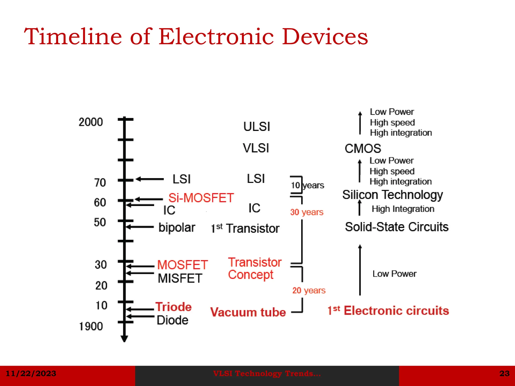
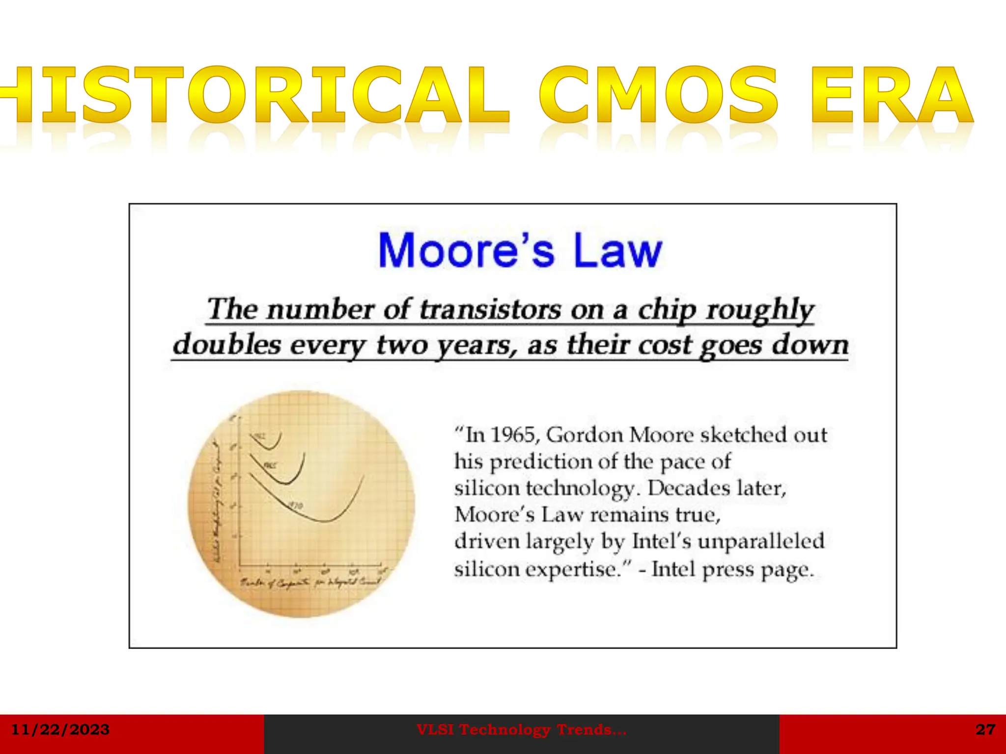
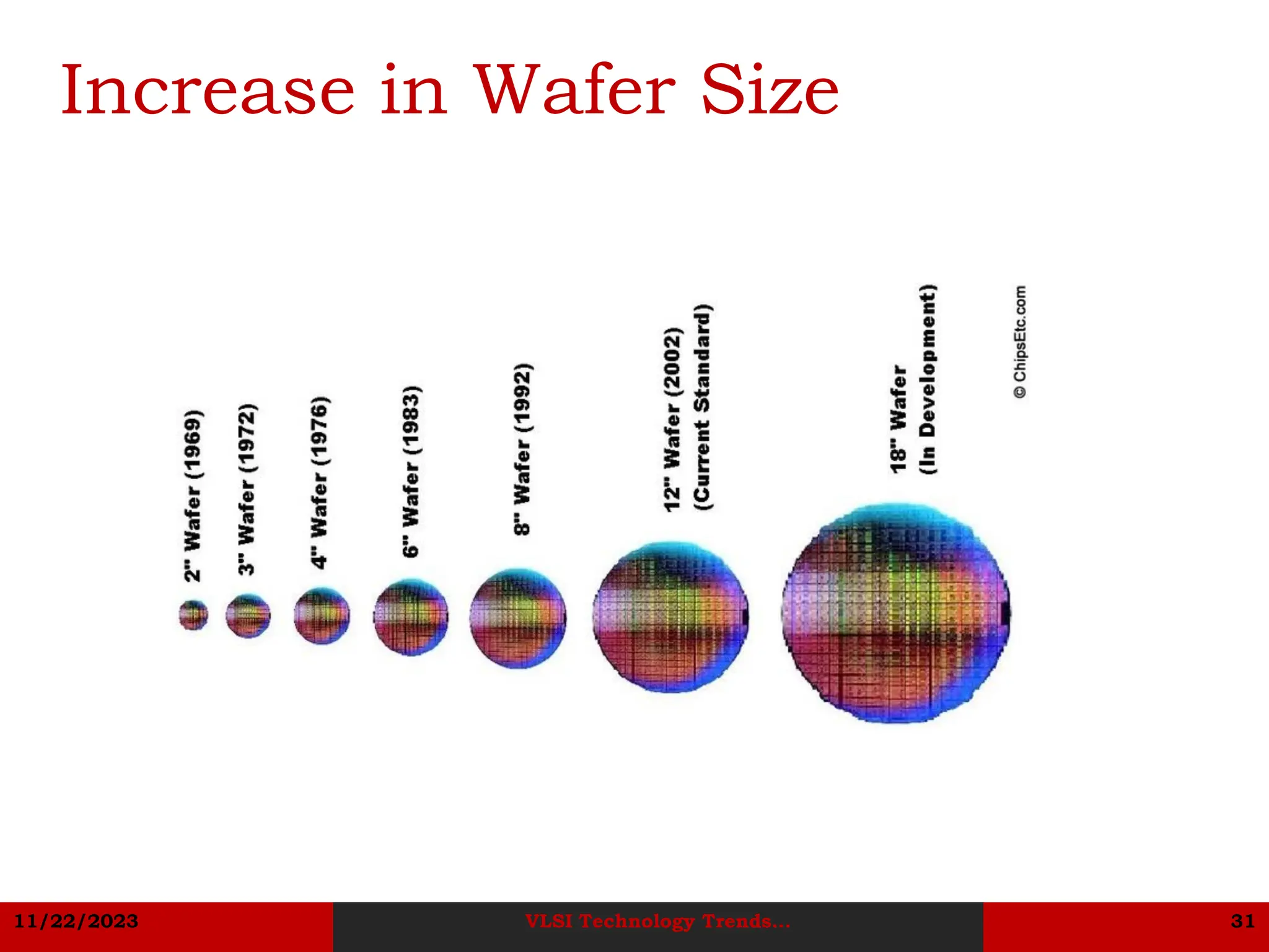
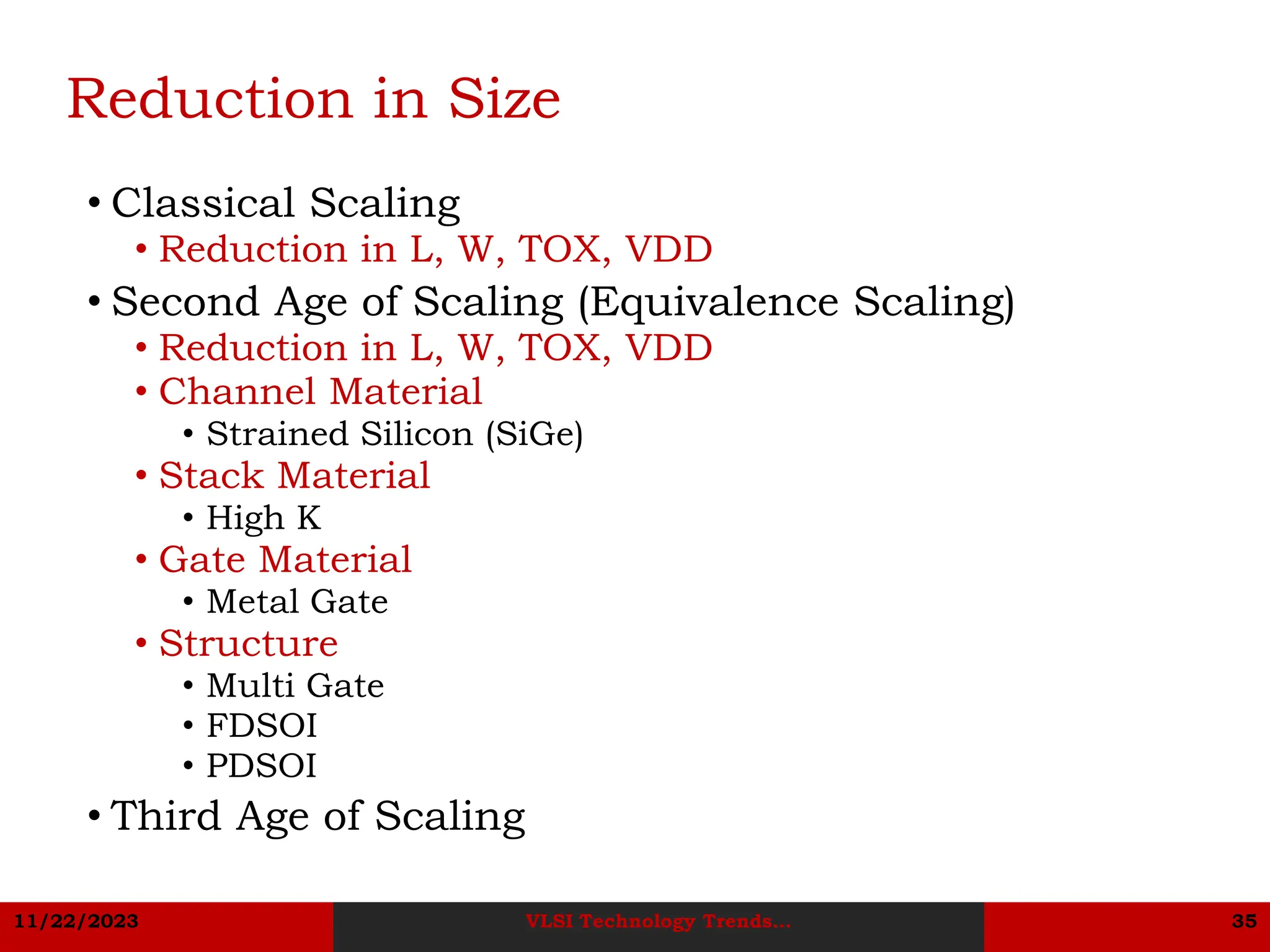
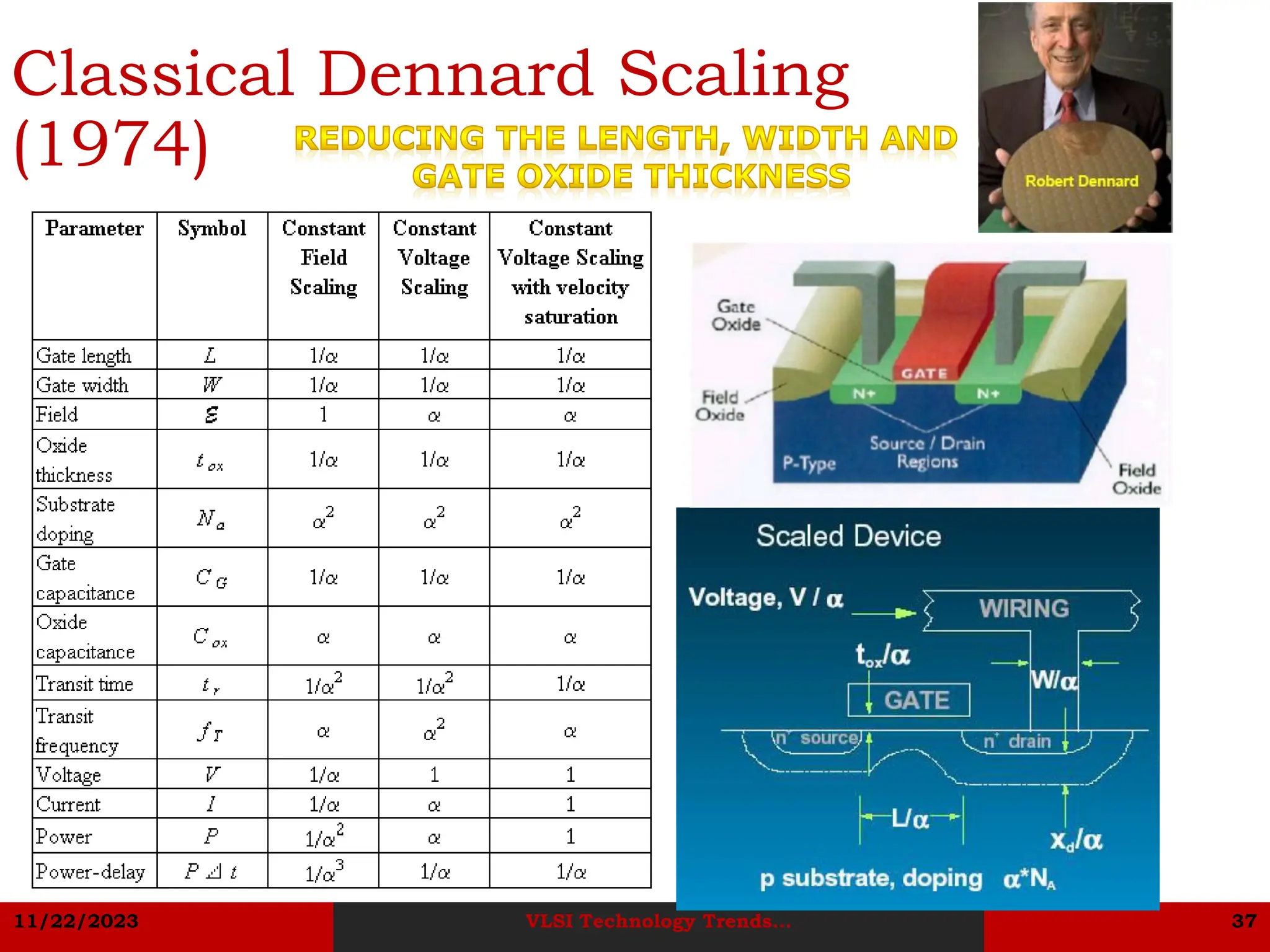
11/22/2023 VLSI Technology Trends... 1
VLSI Technology Trends….
Dr Usha Mehta
usha.mehta@nirmauni.ac.in
11/22/2023 VLSI Technology Trends... 2
Acknowledgement
This presentation has been summarized from various
books, papers, websites and presentations on VLSI
Design and its various topics all over the world. I
couldn’t remember where these large pull of hints and
work come from. However, I’d like to thank all
professors and scientists who created such a good work
on this emerging field. Without those efforts in this very
emerging technology, these notes and slides can’t be
finished.
NOTE: The figures, text etc included in slides are
borrowed from various books’ websites, authors’ books,
websites, pages and other sources for academic purpose
only. The instructor does not claim any originality.
11/22/2023 VLSI Technology Trends... 3
11/22/2023 VLSI Technology Trends... 4
What if other things in life also followed the
transistor’s path?
Courtesy: www.news18.com
11/22/2023 VLSI Technology Trends... 5
What if other things in life also followed the
transistor’s path?
Courtesy: www.news18.com
11/22/2023 VLSI Technology Trends... 6
What if other things in life also followed the
transistor’s path?
Courtesy: www.news18.com
11/22/2023 VLSI Technology Trends... 7
Cost of Transistor
11/22/2023 VLSI Technology Trends... 8
11/22/2023 VLSI Technology Trends... 9
11/22/2023 VLSI Technology Trends... 10
Supply Chain of Semiconductor World
11/22/2023 VLSI Technology Trends... 11
VLSI Companies in India
11/22/2023 VLSI Technology Trends... 12
11/22/2023 VLSI Technology Trends... 13
The first Computer ENIAC using Valve
and Relays
• May 1944
• first ever general purpose electronic
computer
• by a team lead by J.P.Eckert and
J.W.Mauchly
• more than 18,000 valves, 100 by 10
by 3 feet, weight 30 tons.
• Faster than anything that had been
built previously; multiplication in
under 3 ms.
• Described as being “Faster than
thought”.
11/22/2023 VLSI Technology Trends... 14
The most important invention in 20th
Century
11/22/2023 VLSI Technology Trends... 15
The First Bipolar Transistor
• 1947: Point Contact Bipolar Transistor
• 1948: Junction Bipolar Transistor
• Bardeen, Brattain, Shockley
• -Bell Lab
11/22/2023 VLSI Technology Trends... 16
William Shockley and John Bardeen :
accepting their noble prizes on December 10, 1956
11/22/2023 VLSI Technology Trends... 17
Research vs. Failure
11/22/2023 VLSI Technology Trends... 18
Field Effect Transistor (1928)
concept –much earlier then implementation
11/22/2023 VLSI Technology Trends... 19
Shockley’s Patent Note book (1945)
11/22/2023 VLSI Technology Trends... 20
History of Integrated Circuit
• 1958: 1st Integrated Circuit
• Jack Kilby
• Texas Instruments
Noble Prize in 2000
11/22/2023 VLSI Technology Trends... 21
History of Integrated Circuit…..cont…
• 1959: 1st Planner(2D) Integrated Circuit
• Robert Noyce
• Fairchild Semiconductor
11/22/2023 VLSI Technology Trends... 22
History of MOS
• 1960: 1st MOSFET
• D Kahng and M Atalla
• Bell Lab
11/22/2023 VLSI Technology Trends... 23
Timeline of Electronic Devices
11/22/2023 VLSI Technology Trends... 24
Level of Integration:
Chip Complexity
11/22/2023 VLSI Technology Trends... 25
Digital Logic Families
Si-Ge Silicon-Germanium for RF
11/22/2023 VLSI Technology Trends... 26
IC Fabrication Flow
11/22/2023 VLSI Technology Trends... 27
11/22/2023 VLSI Technology Trends... 28
Is it so…..!!!!!
11/22/2023 VLSI Technology Trends... 29
• Double the No. of transistor per chip:
~50 % Lithography – ability to print smaller
features
~25% bigger chips/wafers
~25% design improvements
11/22/2023 VLSI Technology Trends... 30
Reduction in Transistor Size….
11/22/2023 VLSI Technology Trends... 31
Increase in Wafer Size
11/22/2023 VLSI Technology Trends... 32
Technology Windows
• Micron Technology
• Greater than or equal to 1
μm
• Sub-Micron (SM)
Technology
• 0.8 μm
• 0.6 μm
• 0.5 μm
• Deep Sub-Micron
Technology (DSM)
• 0.35 μm
• 0.25 μm
• 0.18 μm
• Ultra Deep Sub-Micron
Technology(UDSM)
• 0.15 μm
• 0.13 μm
• Nanometer Technology
• 90 nm
• 65 nm
• 32 nm
• 28 nm
• 22 nm
• 14nm
• 10nm
• 7nm
• 5nm
11/22/2023 VLSI Technology Trends... 33
Why Moore’s Law sustained?
(point of view:1)
•Lowest cost
•Maximum Functions
•Smallest size
•highest speed
•Long lasting battery
•More reliable
11/22/2023 VLSI Technology Trends... 34
Why Moore’s Law sustained…..?
(point of view:2)
Transistor
Scaling
Better
Performance
Market Growth
Investment
11/22/2023 VLSI Technology Trends... 35
Reduction in Size
• Classical Scaling
• Reduction in L, W, TOX, VDD
• Second Age of Scaling (Equivalence Scaling)
• Reduction in L, W, TOX, VDD
• Channel Material
• Strained Silicon (SiGe)
• Stack Material
• High K
• Gate Material
• Metal Gate
• Structure
• Multi Gate
• FDSOI
• PDSOI
• Third Age of Scaling
11/22/2023 VLSI Technology Trends... 36
11/22/2023 VLSI Technology Trends... 37
Classical Dennard Scaling
(1974)
11/22/2023 VLSI Technology Trends... 38
• Constant Voltage
Scaling
• Vdd constant
• More preferable
because of
peripherals
• Power consumption
increases by …..
• Power density
increases by 3
• Constant Field Scaling
• Seems ideal but Not a
feasible option
• to keep new chips
compatible with existing
chips, voltages cannot be
scaled arbitrarily.
• Peripherals require
certain voltage levels at
inputs and outputs
• Multiple supply voltages
• Complicated Level shifter
arrangement
11/22/2023 VLSI Technology Trends... 39
Effects of Scaling
• Short Channel Effects
• Narrow channel Effects
• Subthreshold Conduction
• Punch through
• Hot electrons/hot carriers
• Electromigration
• ESD
• Electric Overstress…..
11/22/2023 VLSI Technology Trends... 40
• In view of number of road blocks in standard CMOS
scaling, new device architectures were adopted in
second generation of scaling.
11/22/2023 VLSI Technology Trends... 41
Strained MOSFET
• Because of constant voltage scaling, the electric field is
increased. Strong vertical fields resulting from large Vgs cause
the carriers to scatter against the surface and also reduce the
carrier mobility. This effect is called mobility degradation
• The links between the silicon atoms become stretched - thereby
leading to strained silicon. Moving these silicon atoms farther
apart reduces the atomic forces that interfere with the
movement of electrons through the transistors and thus
better mobility
11/22/2023 VLSI Technology Trends... 42
Limitation….
• Gate Oxide thickness can not be scaled down beyond a
limit because
• Processing difficulties in growing thin uniform oxide layer (
nonuniform oxide growth “pinholes” causes shorts between
gate and substrate)
• Oxide breakdown
• Thickness of SiO₂ layer required in 45nm technology is
about 1.2nm (4 atom layers deep!!)
• Gate oxide is running out of atoms
• Quantum nature of channel electron dominates.
• Tunnelling/leakage current IG
11/22/2023 VLSI Technology Trends... 43
High K Material
• If Gate Oxide thickness can not be reduced, can we
increase the quality of gate oxide to give higher
capacitance at same thickness?
• High K Material for gate oxide to increase the
insulator capacitance while keeping a thicker
oxide..
• to avoid tunnelling through the gate oxide
11/22/2023 VLSI Technology Trends... 44
Low K Material
( not in transistors but….)
11/22/2023 VLSI Technology Trends... 45
Metal-Polysilicon-Metal
• Earlier : Metal Gate
• Earlier at 5V supply, metal gates were used
• Then: Polysilicon Gate
• At lower voltages and scaling, polysilicon gate used
because of fabrication process ease.
• After initial doping, very high temp. annealing was
required during which metal gates would melt
• Again: Metal Gate
• When SiO2 is replaced with High-K material, it was
found that PolySi and High K Material were not
compatible, So polySi was replaced by metal.
• After 45nm (Intel) and 28nm (TSMC), again back to
metal gates
• To avoid poly-depletion at the poly oxide interface.
• At smaller scales, the need for a higher Vt has become
important again due to problems of leakage.
11/22/2023 VLSI Technology Trends... 46
HKMG MOSFET
• Intel’s announcement, January 26, 2007
• Hafnium-based high-k material
• Effective Oxide Thickness = 1nm
• Specific gate metals ( Intel’s trade secret)
• Different Metals for NMOS and PMOS
• Use of 193nm dry lithography
• From 65 nm to 45 nm Tech.
• Tr density: 2 times increase
• Tr switching power: 30% reduction
• Tr switching speed: 20% improvement
• S-D leakage power: 5 times reduction
• Gate oxide leakage: 10 times reduction
• 45nm processors (Core™2 family processors "Penryn")
running Windows* Vista*, Linux* etc.
11/22/2023 VLSI Technology Trends... 47
Silicon-on-Insulator (SoI)
• Lower parasitic capacitance due to
isolation from the bulk silicon,
• Resistance to latch up due to complete
isolation of the n- and p-well structures.
• Higher performance at equivalentVDD
• Reduced temperature dependency due to no doping.
• Better yield due to high density, better wafer utilization.
• Reduced antenna issues
• No body or well taps are needed.
• Lower leakage currents due to isolation thus higher
power efficiency.
• Inherently radiation hardened ( resistant to soft errors ),
thus reducing the need for redundancy.
11/22/2023 VLSI Technology Trends... 48
FDSOI
•Fully Depleted
•Very thin layer of
buried oxide
•The region under the
channel is fully
depleted no neutral
region exists.
PDSOI
•Partially Depleted
•Thick layer of
Buried oxide
•Neutral regions
exists under
channel
•Floating body
effect
11/22/2023 VLSI Technology Trends... 49
Industry use of SoI
• IBM : "Istar" PowerPC-AS microprocessor
• AMD : 130 nm, 90 nm, 65 nm, 45 nm and 32 nm
single, dual, quad, six and eight core processor
• FreeScale: PowerPC 7455 CPU
• Intel did not use SoI in general but moved to HKMG
and Trigate with Conventional CMOS
• As for the traditional foundries, on July 2006, TSMC
claimed no customer wanted SOI
11/22/2023 VLSI Technology Trends... 50
Still this is not enough…..
• How should be ideal transistor?
11/22/2023 VLSI Technology Trends... 51
How SoI to Double Gate
11/22/2023 VLSI Technology Trends... 52
Double Gate to Tri-Gate
11/22/2023 VLSI Technology Trends... 53
Gate Architectures
11/22/2023 VLSI Technology Trends... 54
Tri-gate Transistor
11/22/2023 VLSI Technology Trends... 55
Tri-gate SoI Transistor
11/22/2023 VLSI Technology Trends... 56
FinFET vs. Tri-gate
• FinFET
• Spacer
• So dual gated side gate
• Trigate
• Triple side gate
• Easy fabrication
• Improved
manufacturability
11/22/2023 VLSI Technology Trends... 57
FinFET
11/22/2023 VLSI Technology Trends... 58
FinFET
11/22/2023 VLSI Technology Trends... 59
11/22/2023 VLSI Technology Trends... 60
All Around Gate Transistor
11/22/2023 VLSI Technology Trends... 61
Transistor Pathway
11/22/2023 VLSI Technology Trends... 62
Further Shrinking….
11/22/2023 VLSI Technology Trends... 63
•https://slideplayer.com/slide/1653483/
11/22/2023 VLSI Technology Trends... 64
11/22/2023 VLSI Technology Trends... 65
11/22/2023 VLSI Technology Trends... 66
11/22/2023 VLSI Technology Trends... 67
11/22/2023 VLSI Technology Trends... 68
11/22/2023 VLSI Technology Trends... 69
11/22/2023 VLSI Technology Trends... 70
11/22/2023 VLSI Technology Trends... 71
11/22/2023 VLSI Technology Trends... 72
11/22/2023 VLSI Technology Trends... 73
11/22/2023 VLSI Technology Trends... 74
•More Moore:
•continuous scaling,
•Already up to 7 or 5nm
•Beyond CMOS:
•new technologies such as graphene
•nanowires from the area of
Nanosciences and Nanotechnologies
•More than Moore:
•additional functionalities such as
micro/nanosystem, RF, analog, biochips
on more conventional logic or memory
circuits
11/22/2023 VLSI Technology Trends... 75
ITRS Roadmap
11/22/2023 VLSI Technology Trends... 76
Roadmap for Century…..
Courtesy: H. Iwai, Microelectronics. Eng. (2009), doi:10.1016/j.mee.2009.03
11/22/2023 VLSI Technology Trends... 77
Adopt Natural Bio System….
Just for example, brain of the mosquito make the real
time 3D flight control with image processing equipped
with many sensors such as infrared and CO2 with
extremely small brain volume and extremely small
energy consumption. The performance of dragonfly’s
brain is much higher. Today’s performance and energy
consumption of the microprocessor are not comparable
to those of insect brains, at all. Introduction of the
algorithm of the bio system will be the ultimate method
in the roadmap.
11/22/2023 VLSI Technology Trends... 78
Thank you!

5_DVD_VLSI Technology Trends.pdf

  • 1.
    11/22/2023 VLSI TechnologyTrends... 1 VLSI Technology Trends…. Dr Usha Mehta usha.mehta@nirmauni.ac.in
  • 2.
    11/22/2023 VLSI TechnologyTrends... 2 Acknowledgement This presentation has been summarized from various books, papers, websites and presentations on VLSI Design and its various topics all over the world. I couldn’t remember where these large pull of hints and work come from. However, I’d like to thank all professors and scientists who created such a good work on this emerging field. Without those efforts in this very emerging technology, these notes and slides can’t be finished. NOTE: The figures, text etc included in slides are borrowed from various books’ websites, authors’ books, websites, pages and other sources for academic purpose only. The instructor does not claim any originality.
  • 3.
  • 4.
    11/22/2023 VLSI TechnologyTrends... 4 What if other things in life also followed the transistor’s path? Courtesy: www.news18.com
  • 5.
    11/22/2023 VLSI TechnologyTrends... 5 What if other things in life also followed the transistor’s path? Courtesy: www.news18.com
  • 6.
    11/22/2023 VLSI TechnologyTrends... 6 What if other things in life also followed the transistor’s path? Courtesy: www.news18.com
  • 7.
    11/22/2023 VLSI TechnologyTrends... 7 Cost of Transistor
  • 8.
  • 9.
  • 10.
    11/22/2023 VLSI TechnologyTrends... 10 Supply Chain of Semiconductor World
  • 11.
    11/22/2023 VLSI TechnologyTrends... 11 VLSI Companies in India
  • 12.
  • 13.
    11/22/2023 VLSI TechnologyTrends... 13 The first Computer ENIAC using Valve and Relays • May 1944 • first ever general purpose electronic computer • by a team lead by J.P.Eckert and J.W.Mauchly • more than 18,000 valves, 100 by 10 by 3 feet, weight 30 tons. • Faster than anything that had been built previously; multiplication in under 3 ms. • Described as being “Faster than thought”.
  • 14.
    11/22/2023 VLSI TechnologyTrends... 14 The most important invention in 20th Century
  • 15.
    11/22/2023 VLSI TechnologyTrends... 15 The First Bipolar Transistor • 1947: Point Contact Bipolar Transistor • 1948: Junction Bipolar Transistor • Bardeen, Brattain, Shockley • -Bell Lab
  • 16.
    11/22/2023 VLSI TechnologyTrends... 16 William Shockley and John Bardeen : accepting their noble prizes on December 10, 1956
  • 17.
    11/22/2023 VLSI TechnologyTrends... 17 Research vs. Failure
  • 18.
    11/22/2023 VLSI TechnologyTrends... 18 Field Effect Transistor (1928) concept –much earlier then implementation
  • 19.
    11/22/2023 VLSI TechnologyTrends... 19 Shockley’s Patent Note book (1945)
  • 20.
    11/22/2023 VLSI TechnologyTrends... 20 History of Integrated Circuit • 1958: 1st Integrated Circuit • Jack Kilby • Texas Instruments Noble Prize in 2000
  • 21.
    11/22/2023 VLSI TechnologyTrends... 21 History of Integrated Circuit…..cont… • 1959: 1st Planner(2D) Integrated Circuit • Robert Noyce • Fairchild Semiconductor
  • 22.
    11/22/2023 VLSI TechnologyTrends... 22 History of MOS • 1960: 1st MOSFET • D Kahng and M Atalla • Bell Lab
  • 23.
    11/22/2023 VLSI TechnologyTrends... 23 Timeline of Electronic Devices
  • 24.
    11/22/2023 VLSI TechnologyTrends... 24 Level of Integration: Chip Complexity
  • 25.
    11/22/2023 VLSI TechnologyTrends... 25 Digital Logic Families Si-Ge Silicon-Germanium for RF
  • 26.
    11/22/2023 VLSI TechnologyTrends... 26 IC Fabrication Flow
  • 27.
  • 28.
    11/22/2023 VLSI TechnologyTrends... 28 Is it so…..!!!!!
  • 29.
    11/22/2023 VLSI TechnologyTrends... 29 • Double the No. of transistor per chip: ~50 % Lithography – ability to print smaller features ~25% bigger chips/wafers ~25% design improvements
  • 30.
    11/22/2023 VLSI TechnologyTrends... 30 Reduction in Transistor Size….
  • 31.
    11/22/2023 VLSI TechnologyTrends... 31 Increase in Wafer Size
  • 32.
    11/22/2023 VLSI TechnologyTrends... 32 Technology Windows • Micron Technology • Greater than or equal to 1 μm • Sub-Micron (SM) Technology • 0.8 μm • 0.6 μm • 0.5 μm • Deep Sub-Micron Technology (DSM) • 0.35 μm • 0.25 μm • 0.18 μm • Ultra Deep Sub-Micron Technology(UDSM) • 0.15 μm • 0.13 μm • Nanometer Technology • 90 nm • 65 nm • 32 nm • 28 nm • 22 nm • 14nm • 10nm • 7nm • 5nm
  • 33.
    11/22/2023 VLSI TechnologyTrends... 33 Why Moore’s Law sustained? (point of view:1) •Lowest cost •Maximum Functions •Smallest size •highest speed •Long lasting battery •More reliable
  • 34.
    11/22/2023 VLSI TechnologyTrends... 34 Why Moore’s Law sustained…..? (point of view:2) Transistor Scaling Better Performance Market Growth Investment
  • 35.
    11/22/2023 VLSI TechnologyTrends... 35 Reduction in Size • Classical Scaling • Reduction in L, W, TOX, VDD • Second Age of Scaling (Equivalence Scaling) • Reduction in L, W, TOX, VDD • Channel Material • Strained Silicon (SiGe) • Stack Material • High K • Gate Material • Metal Gate • Structure • Multi Gate • FDSOI • PDSOI • Third Age of Scaling
  • 36.
  • 37.
    11/22/2023 VLSI TechnologyTrends... 37 Classical Dennard Scaling (1974)
  • 38.
    11/22/2023 VLSI TechnologyTrends... 38 • Constant Voltage Scaling • Vdd constant • More preferable because of peripherals • Power consumption increases by ….. • Power density increases by 3 • Constant Field Scaling • Seems ideal but Not a feasible option • to keep new chips compatible with existing chips, voltages cannot be scaled arbitrarily. • Peripherals require certain voltage levels at inputs and outputs • Multiple supply voltages • Complicated Level shifter arrangement
  • 39.
    11/22/2023 VLSI TechnologyTrends... 39 Effects of Scaling • Short Channel Effects • Narrow channel Effects • Subthreshold Conduction • Punch through • Hot electrons/hot carriers • Electromigration • ESD • Electric Overstress…..
  • 40.
    11/22/2023 VLSI TechnologyTrends... 40 • In view of number of road blocks in standard CMOS scaling, new device architectures were adopted in second generation of scaling.
  • 41.
    11/22/2023 VLSI TechnologyTrends... 41 Strained MOSFET • Because of constant voltage scaling, the electric field is increased. Strong vertical fields resulting from large Vgs cause the carriers to scatter against the surface and also reduce the carrier mobility. This effect is called mobility degradation • The links between the silicon atoms become stretched - thereby leading to strained silicon. Moving these silicon atoms farther apart reduces the atomic forces that interfere with the movement of electrons through the transistors and thus better mobility
  • 42.
    11/22/2023 VLSI TechnologyTrends... 42 Limitation…. • Gate Oxide thickness can not be scaled down beyond a limit because • Processing difficulties in growing thin uniform oxide layer ( nonuniform oxide growth “pinholes” causes shorts between gate and substrate) • Oxide breakdown • Thickness of SiO₂ layer required in 45nm technology is about 1.2nm (4 atom layers deep!!) • Gate oxide is running out of atoms • Quantum nature of channel electron dominates. • Tunnelling/leakage current IG
  • 43.
    11/22/2023 VLSI TechnologyTrends... 43 High K Material • If Gate Oxide thickness can not be reduced, can we increase the quality of gate oxide to give higher capacitance at same thickness? • High K Material for gate oxide to increase the insulator capacitance while keeping a thicker oxide.. • to avoid tunnelling through the gate oxide
  • 44.
    11/22/2023 VLSI TechnologyTrends... 44 Low K Material ( not in transistors but….)
  • 45.
    11/22/2023 VLSI TechnologyTrends... 45 Metal-Polysilicon-Metal • Earlier : Metal Gate • Earlier at 5V supply, metal gates were used • Then: Polysilicon Gate • At lower voltages and scaling, polysilicon gate used because of fabrication process ease. • After initial doping, very high temp. annealing was required during which metal gates would melt • Again: Metal Gate • When SiO2 is replaced with High-K material, it was found that PolySi and High K Material were not compatible, So polySi was replaced by metal. • After 45nm (Intel) and 28nm (TSMC), again back to metal gates • To avoid poly-depletion at the poly oxide interface. • At smaller scales, the need for a higher Vt has become important again due to problems of leakage.
  • 46.
    11/22/2023 VLSI TechnologyTrends... 46 HKMG MOSFET • Intel’s announcement, January 26, 2007 • Hafnium-based high-k material • Effective Oxide Thickness = 1nm • Specific gate metals ( Intel’s trade secret) • Different Metals for NMOS and PMOS • Use of 193nm dry lithography • From 65 nm to 45 nm Tech. • Tr density: 2 times increase • Tr switching power: 30% reduction • Tr switching speed: 20% improvement • S-D leakage power: 5 times reduction • Gate oxide leakage: 10 times reduction • 45nm processors (Core™2 family processors "Penryn") running Windows* Vista*, Linux* etc.
  • 47.
    11/22/2023 VLSI TechnologyTrends... 47 Silicon-on-Insulator (SoI) • Lower parasitic capacitance due to isolation from the bulk silicon, • Resistance to latch up due to complete isolation of the n- and p-well structures. • Higher performance at equivalentVDD • Reduced temperature dependency due to no doping. • Better yield due to high density, better wafer utilization. • Reduced antenna issues • No body or well taps are needed. • Lower leakage currents due to isolation thus higher power efficiency. • Inherently radiation hardened ( resistant to soft errors ), thus reducing the need for redundancy.
  • 48.
    11/22/2023 VLSI TechnologyTrends... 48 FDSOI •Fully Depleted •Very thin layer of buried oxide •The region under the channel is fully depleted no neutral region exists. PDSOI •Partially Depleted •Thick layer of Buried oxide •Neutral regions exists under channel •Floating body effect
  • 49.
    11/22/2023 VLSI TechnologyTrends... 49 Industry use of SoI • IBM : "Istar" PowerPC-AS microprocessor • AMD : 130 nm, 90 nm, 65 nm, 45 nm and 32 nm single, dual, quad, six and eight core processor • FreeScale: PowerPC 7455 CPU • Intel did not use SoI in general but moved to HKMG and Trigate with Conventional CMOS • As for the traditional foundries, on July 2006, TSMC claimed no customer wanted SOI
  • 50.
    11/22/2023 VLSI TechnologyTrends... 50 Still this is not enough….. • How should be ideal transistor?
  • 51.
    11/22/2023 VLSI TechnologyTrends... 51 How SoI to Double Gate
  • 52.
    11/22/2023 VLSI TechnologyTrends... 52 Double Gate to Tri-Gate
  • 53.
    11/22/2023 VLSI TechnologyTrends... 53 Gate Architectures
  • 54.
    11/22/2023 VLSI TechnologyTrends... 54 Tri-gate Transistor
  • 55.
    11/22/2023 VLSI TechnologyTrends... 55 Tri-gate SoI Transistor
  • 56.
    11/22/2023 VLSI TechnologyTrends... 56 FinFET vs. Tri-gate • FinFET • Spacer • So dual gated side gate • Trigate • Triple side gate • Easy fabrication • Improved manufacturability
  • 57.
    11/22/2023 VLSI TechnologyTrends... 57 FinFET
  • 58.
    11/22/2023 VLSI TechnologyTrends... 58 FinFET
  • 59.
  • 60.
    11/22/2023 VLSI TechnologyTrends... 60 All Around Gate Transistor
  • 61.
    11/22/2023 VLSI TechnologyTrends... 61 Transistor Pathway
  • 62.
    11/22/2023 VLSI TechnologyTrends... 62 Further Shrinking….
  • 63.
    11/22/2023 VLSI TechnologyTrends... 63 •https://slideplayer.com/slide/1653483/
  • 64.
  • 65.
  • 66.
  • 67.
  • 68.
  • 69.
  • 70.
  • 71.
  • 72.
  • 73.
  • 74.
    11/22/2023 VLSI TechnologyTrends... 74 •More Moore: •continuous scaling, •Already up to 7 or 5nm •Beyond CMOS: •new technologies such as graphene •nanowires from the area of Nanosciences and Nanotechnologies •More than Moore: •additional functionalities such as micro/nanosystem, RF, analog, biochips on more conventional logic or memory circuits
  • 75.
    11/22/2023 VLSI TechnologyTrends... 75 ITRS Roadmap
  • 76.
    11/22/2023 VLSI TechnologyTrends... 76 Roadmap for Century….. Courtesy: H. Iwai, Microelectronics. Eng. (2009), doi:10.1016/j.mee.2009.03
  • 77.
    11/22/2023 VLSI TechnologyTrends... 77 Adopt Natural Bio System…. Just for example, brain of the mosquito make the real time 3D flight control with image processing equipped with many sensors such as infrared and CO2 with extremely small brain volume and extremely small energy consumption. The performance of dragonfly’s brain is much higher. Today’s performance and energy consumption of the microprocessor are not comparable to those of insect brains, at all. Introduction of the algorithm of the bio system will be the ultimate method in the roadmap.
  • 78.
    11/22/2023 VLSI TechnologyTrends... 78 Thank you!