Downloaded 275 times
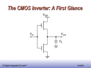
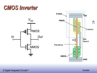
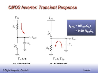

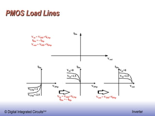
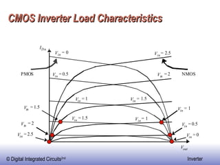
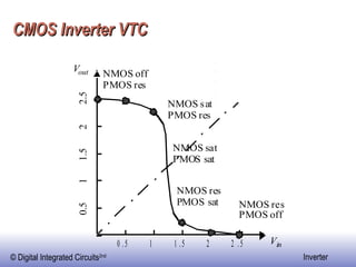
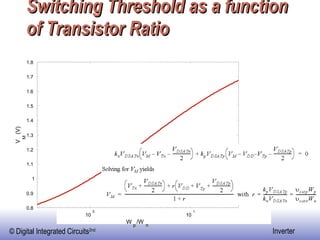
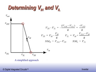
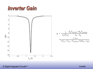
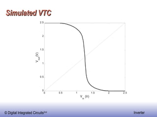

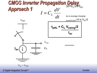
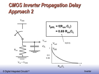
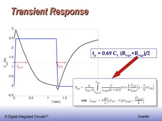
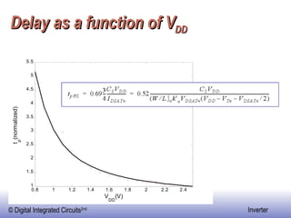
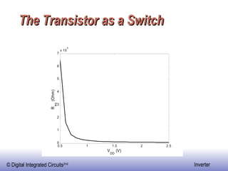

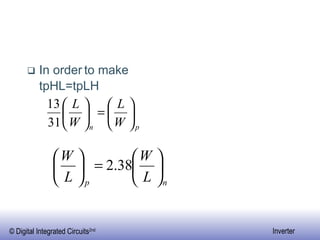
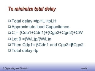
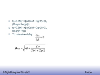
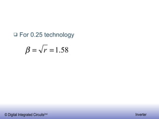
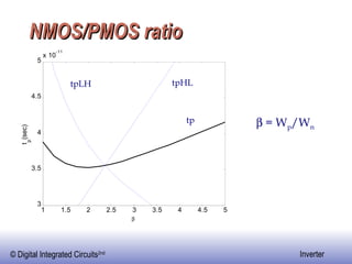

The document discusses the CMOS inverter, including its basic structure and operation, transient response characteristics, voltage transfer curve, propagation delay, and design considerations for improving performance such as minimizing delay. It provides analysis of how varying factors like transistor widths, supply voltage, and load capacitance affect the inverter's switching threshold, rise/fall times, and propagation delay. The goal of the analysis is to determine the optimal transistor width ratios and device parameters needed to design a high-performance symmetric CMOS inverter with minimum total propagation delay.