Downloaded 1,307 times
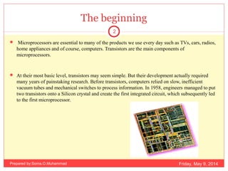

The document provides an overview of Very Large Scale Integration (VLSI) and its significance in the development of microprocessors, essential components in everyday electronics. It traces the evolution of microprocessors from early computers reliant on vacuum tubes to modern integrated circuits, showcasing the advancement in technology and the miniaturization of components. VLSI technology, which allows thousands of transistors to be combined on a single chip, has played a crucial role in enhancing computer performance, reducing costs, and expanding their applications across various devices.