Downloaded 175 times

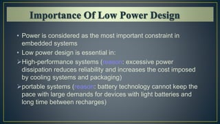
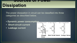

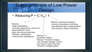
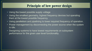
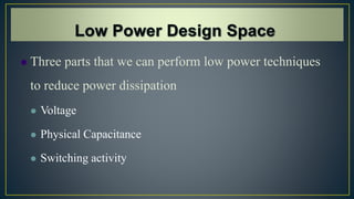
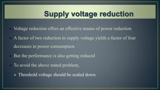
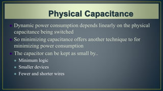
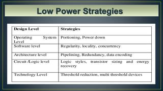
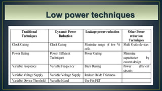


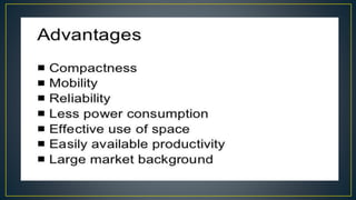

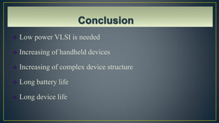


Low power VLSI design has become important due to increasing integration leading to higher power consumption. Low power design is essential for handheld devices to allow long battery life and better performance. There are various techniques for low power design including reducing supply voltage, minimizing capacitance and switching activity, and employing strategies like clock gating and power gating. Low power design can be achieved at different levels from system to logic to physical design.