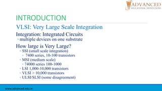
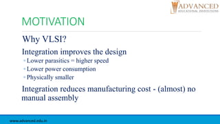
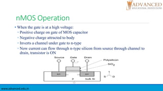
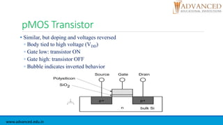
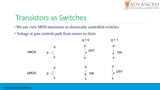
VLSI Technology
- A Design Perspective
BY
PRIYANKA GAUR
ASSISTANT PROFESSOR (DEPT. OF ECE)
www.advanced.edu.in
OUTLINE
www.advanced.edu.in
•Introduction
•Motivation
•VLSI design process
•Semiconductor and doping
•Details of MOS transistor
•nMOS transistor and operation
•pMOS transistor
•Transistor as switches
•CMOS Technology
•VLSI applications
INTRODUCTION
VLSI: Very Large Scale Integration
Integration: Integrated Circuits
◦ multiple devices on one substrate
How large is Very Large?
◦ SSI (small scale integration)
◦ 7400 series, 10-100 transistors
◦ MSI (medium scale)
◦ 74000 series 100-1000
◦ LSI 1,000-10,000 transistors
◦ VLSI > 10,000 transistors
◦ ULSI/SLSI (some disagreement)
www.advanced.edu.in
MOTIVATION
Why VLSI?
Integration improves the design
◦ Lower parasitics = higher speed
◦ Lower power consumption
◦ Physically smaller
Integration reduces manufacturing cost - (almost) no
manual assembly
www.advanced.edu.in
Moore’s Law
• Gordon Moore: co-founder of Intel
•Predicted that the number of transistors per chip
would grow exponentially (double every 18 months)
•Exponential improvement in technology is a natural
trend:
◦e.g. Steam Engines - Dynamo - Automobile
www.advanced.edu.in
VLSI Design Process
What is a Silicon Chip?
• A pattern of interconnected switches and gates on the surface of a crystal
of semiconductor (typically Si)
• These switches and gates are made of
◦ areas of n-type silicon
◦ areas of p-type silicon
◦ areas of insulator
◦ lines of conductor (interconnects) joining areas together
◦ Aluminium, Copper, Titanium, Molybdenum, polysilicon, tungsten
• The geometry of these areas is known as the layout of the chip
• Connections from the chip to the outside world are made around the edge
of the chip to facilitate connections to other devices
www.advanced.edu.in
VLSI Design Process
Switches
• Digital equipment is largely composed of switches
• Switches can be built from many technologies
◦ relays (from which the earliest computers were built)
◦ thermionic valves
◦ transistors
• The perfect digital switch would have the following:
◦ switch instantly
◦ use no power
◦ have an infinite resistance when off and zero resistance when on
• Real switches are not like this!
www.advanced.edu.in
Semiconductors and Doping
• Adding trace amounts of certain materials to semiconductors alters the
crystal structure and can change their electrical properties
◦ in particular it can change the number of free electrons or holes
• N-Type
◦ semiconductor has free electrons
◦ dopant is (typically) phosphorus, arsenic, antimony
• P-Type
◦ semiconductor has free holes
◦ dopant is (typically) boron, indium, gallium
• Dopants are usually implanted into the semiconductor using Implant
Technology, followed by thermal process to diffuse the dopants
www.advanced.edu.in
Basic MOS Transistors
Minimum line width
Transistor cross section
Charge inversion channel
Source connected to substrate
Enhancement vs. Depletion mode devices
p-MOS are 2.5 time slower than n-MOS due to electron and hole
mobilities
www.advanced.edu.in
The Process of VLSI Design:
• Consists of many different representations/Abstractions of the
system (chip) that is being designed.
◦ System Level Design
◦ Architecture / Algorithm Level Design
◦ Digital System Level Design
◦ Logical Level Design
◦ Electrical Level Design
◦ Layout Level Design
◦ Semiconductor Level Design (possibly more)
• Each abstraction/view is itself a Design Hierarchy of
refinements which decompose the design.
www.advanced.edu.in
Design Abstraction Levels
n+n+
S
G
D
+
DEVICE
CIRCUIT
GATE
MODULE
SYSTEM
www.advanced.edu.in
Fabrication Technology
• Silicon of extremely high purity
◦ chemically purified then grown into large crystals
• Wafers
◦ crystals are sliced into wafers
◦ wafer diameter is currently 150mm, 200mm, 300mm
◦ wafer thickness <1mm
◦ surface is polished to optical smoothness
• Wafer is then ready for processing
• Each wafer will yield many chips
◦ chip die size varies from about 5mmx5mm to 15mmx15mm
◦ A whole wafer is processed at a time
www.advanced.edu.in
Fabrication Technology
Different parts of each die will be made P-type or N-type (small
amount of other atoms intentionally introduced - doping -implant)
Interconnections are made with metal
Insulation used is typically SiO2. SiN is also used. New materials
being investigated (low-k dielectrics)
nMOS Fabrication
CMOS Fabrication
p-well process
n-well process
twin-tub process
www.advanced.edu.in
Fabrication Technology
• All the devices on the wafer are made at the same time
• After the circuitry has been placed on the chip
◦ the chip is over-glassed (with a passivation layer) to protect it
◦ only those areas which connect to the outside world will be left uncovered (the pads)
• The wafer finally passes to a test station
◦ test probes send test signal patterns to the chip and monitor the output of the chip
• The yield of a process is the percentage of die which pass this testing
• The wafer is then scribed and separated up into the individual chips. These
are then packaged
• Chips are ‘binned’ according to their performance
www.advanced.edu.in
nMOS Transistor
• Four terminals: gate, source, drain, body
• Gate – oxide – body stack looks like a capacitor
◦ Gate and body are conductors
◦ SiO2 (oxide) is a very good insulator
◦ Called metal – oxide – semiconductor (MOS) capacitor
n+
p
GateSource Drain
bulk Si
SiO2
Polysilicon
n+
www.advanced.edu.in
nMOS Operation
• Body is commonly tied to ground (0 V)
• When the gate is at a low voltage:
◦ P-type body is at low voltage
◦ Source-body and drain-body diodes are OFF
◦ No current flows, transistor is OFF
n+
p
GateSource Drain
bulk Si
SiO2
Polysilicon
n+
D
0
S
www.advanced.edu.in
nMOS Operation
• When the gate is at a high voltage:
◦ Positive charge on gate of MOS capacitor
◦ Negative charge attracted to body
◦ Inverts a channel under gate to n-type
◦ Now current can flow through n-type silicon from source through channel to
drain, transistor is ON
n+
p
GateSource Drain
bulk Si
SiO2
Polysilicon
n+
D
1
S
www.advanced.edu.in
pMOS Transistor
• Similar, but doping and voltages reversed
◦ Body tied to high voltage (VDD)
◦ Gate low: transistor ON
◦ Gate high: transistor OFF
◦ Bubble indicates inverted behavior
SiO2
n
GateSource Drain
bulk Si
Polysilicon
p+ p+
www.advanced.edu.in
Power Supply Voltage
 GND = 0 V
 In 1980’s, VDD = 5V
 VDD has decreased in modern processes due to scaling
◦ High VDD would damage modern tiny transistors
◦ Lower VDD saves power (Dynamic power is propotional to
C.VDD
2.f.a)
 VDD = 3.3, 2.5, 1.8, 1.5, 1.2, 1.0, …
www.advanced.edu.in
Transistors as Switches
• We can view MOS transistors as electrically controlled switches
• Voltage at gate controls path from source to drain
g
s
d
g = 0
s
d
g = 1
s
d
g
s
d
s
d
s
d
nMOS
pMOS
OFF
ON
ON
OFF
www.advanced.edu.in
What is “CMOS VLSI”?
◦ MOS = Metal Oxide Semiconductor (This used to mean a Metal
gate over Oxide insulation)
◦ Now we use polycrystalline silicon which is deposited on the
surface of the chip as a gate. We call this “poly” or just “red stuff”
to distinguish it from the body of the chip, the substrate, which is
a single crystal of silicon.
◦ We do use metal (aluminum) for interconnection wires on the
surface of the chip
www.advanced.edu.in
CMOS: Complementary MOS
◦ Means we are using both N-channel and P-channel type
enhancement mode Field Effect Transistors (FETs).
◦ Field Effect- NO current from the controlling electrode into the
output
◦ FET is a voltage controlled current device
◦ BJT is a current controlled current device
◦ N/P Channel - doping of the substrate for increased carriers
(electrons or holes)
www.advanced.edu.in
SUMMARY
• VLSI is an implementation technology for electronic circuitry - analogue or digital
• It is concerned with forming a pattern of interconnected switches and gates on the
surface of a crystal of semiconductor
• Microprocessors
◦ personal computers
◦ microcontrollers
• Memory - DRAM / SRAM
• Special Purpose Processors - ASICS (CD players, DSP applications)
• Optical Switches
• Has made highly sophisticated control systems mass-producable and therefore cheap
www.advanced.edu.in
Contact Information
Priyanka Gaur
Assistant Professor (ECE Department)
priyanka0920@gmail.com
College Address
Advanced Educational Institutions, 70 km Milestone , Mathura road,
Palwal, Aurangabad, Haryana 121105, Palwal
www.advanced.edu.in

Vlsi ppt priyanka

  • 1.
    VLSI Technology - ADesign Perspective BY PRIYANKA GAUR ASSISTANT PROFESSOR (DEPT. OF ECE) www.advanced.edu.in
  • 2.
    OUTLINE www.advanced.edu.in •Introduction •Motivation •VLSI design process •Semiconductorand doping •Details of MOS transistor •nMOS transistor and operation •pMOS transistor •Transistor as switches •CMOS Technology •VLSI applications
  • 3.
    INTRODUCTION VLSI: Very LargeScale Integration Integration: Integrated Circuits ◦ multiple devices on one substrate How large is Very Large? ◦ SSI (small scale integration) ◦ 7400 series, 10-100 transistors ◦ MSI (medium scale) ◦ 74000 series 100-1000 ◦ LSI 1,000-10,000 transistors ◦ VLSI > 10,000 transistors ◦ ULSI/SLSI (some disagreement) www.advanced.edu.in
  • 4.
    MOTIVATION Why VLSI? Integration improvesthe design ◦ Lower parasitics = higher speed ◦ Lower power consumption ◦ Physically smaller Integration reduces manufacturing cost - (almost) no manual assembly www.advanced.edu.in
  • 5.
    Moore’s Law • GordonMoore: co-founder of Intel •Predicted that the number of transistors per chip would grow exponentially (double every 18 months) •Exponential improvement in technology is a natural trend: ◦e.g. Steam Engines - Dynamo - Automobile www.advanced.edu.in
  • 6.
    VLSI Design Process Whatis a Silicon Chip? • A pattern of interconnected switches and gates on the surface of a crystal of semiconductor (typically Si) • These switches and gates are made of ◦ areas of n-type silicon ◦ areas of p-type silicon ◦ areas of insulator ◦ lines of conductor (interconnects) joining areas together ◦ Aluminium, Copper, Titanium, Molybdenum, polysilicon, tungsten • The geometry of these areas is known as the layout of the chip • Connections from the chip to the outside world are made around the edge of the chip to facilitate connections to other devices www.advanced.edu.in
  • 7.
    VLSI Design Process Switches •Digital equipment is largely composed of switches • Switches can be built from many technologies ◦ relays (from which the earliest computers were built) ◦ thermionic valves ◦ transistors • The perfect digital switch would have the following: ◦ switch instantly ◦ use no power ◦ have an infinite resistance when off and zero resistance when on • Real switches are not like this! www.advanced.edu.in
  • 8.
    Semiconductors and Doping •Adding trace amounts of certain materials to semiconductors alters the crystal structure and can change their electrical properties ◦ in particular it can change the number of free electrons or holes • N-Type ◦ semiconductor has free electrons ◦ dopant is (typically) phosphorus, arsenic, antimony • P-Type ◦ semiconductor has free holes ◦ dopant is (typically) boron, indium, gallium • Dopants are usually implanted into the semiconductor using Implant Technology, followed by thermal process to diffuse the dopants www.advanced.edu.in
  • 9.
    Basic MOS Transistors Minimumline width Transistor cross section Charge inversion channel Source connected to substrate Enhancement vs. Depletion mode devices p-MOS are 2.5 time slower than n-MOS due to electron and hole mobilities www.advanced.edu.in
  • 10.
    The Process ofVLSI Design: • Consists of many different representations/Abstractions of the system (chip) that is being designed. ◦ System Level Design ◦ Architecture / Algorithm Level Design ◦ Digital System Level Design ◦ Logical Level Design ◦ Electrical Level Design ◦ Layout Level Design ◦ Semiconductor Level Design (possibly more) • Each abstraction/view is itself a Design Hierarchy of refinements which decompose the design. www.advanced.edu.in
  • 11.
  • 12.
    Fabrication Technology • Siliconof extremely high purity ◦ chemically purified then grown into large crystals • Wafers ◦ crystals are sliced into wafers ◦ wafer diameter is currently 150mm, 200mm, 300mm ◦ wafer thickness <1mm ◦ surface is polished to optical smoothness • Wafer is then ready for processing • Each wafer will yield many chips ◦ chip die size varies from about 5mmx5mm to 15mmx15mm ◦ A whole wafer is processed at a time www.advanced.edu.in
  • 13.
    Fabrication Technology Different partsof each die will be made P-type or N-type (small amount of other atoms intentionally introduced - doping -implant) Interconnections are made with metal Insulation used is typically SiO2. SiN is also used. New materials being investigated (low-k dielectrics) nMOS Fabrication CMOS Fabrication p-well process n-well process twin-tub process www.advanced.edu.in
  • 14.
    Fabrication Technology • Allthe devices on the wafer are made at the same time • After the circuitry has been placed on the chip ◦ the chip is over-glassed (with a passivation layer) to protect it ◦ only those areas which connect to the outside world will be left uncovered (the pads) • The wafer finally passes to a test station ◦ test probes send test signal patterns to the chip and monitor the output of the chip • The yield of a process is the percentage of die which pass this testing • The wafer is then scribed and separated up into the individual chips. These are then packaged • Chips are ‘binned’ according to their performance www.advanced.edu.in
  • 15.
    nMOS Transistor • Fourterminals: gate, source, drain, body • Gate – oxide – body stack looks like a capacitor ◦ Gate and body are conductors ◦ SiO2 (oxide) is a very good insulator ◦ Called metal – oxide – semiconductor (MOS) capacitor n+ p GateSource Drain bulk Si SiO2 Polysilicon n+ www.advanced.edu.in
  • 16.
    nMOS Operation • Bodyis commonly tied to ground (0 V) • When the gate is at a low voltage: ◦ P-type body is at low voltage ◦ Source-body and drain-body diodes are OFF ◦ No current flows, transistor is OFF n+ p GateSource Drain bulk Si SiO2 Polysilicon n+ D 0 S www.advanced.edu.in
  • 17.
    nMOS Operation • Whenthe gate is at a high voltage: ◦ Positive charge on gate of MOS capacitor ◦ Negative charge attracted to body ◦ Inverts a channel under gate to n-type ◦ Now current can flow through n-type silicon from source through channel to drain, transistor is ON n+ p GateSource Drain bulk Si SiO2 Polysilicon n+ D 1 S www.advanced.edu.in
  • 18.
    pMOS Transistor • Similar,but doping and voltages reversed ◦ Body tied to high voltage (VDD) ◦ Gate low: transistor ON ◦ Gate high: transistor OFF ◦ Bubble indicates inverted behavior SiO2 n GateSource Drain bulk Si Polysilicon p+ p+ www.advanced.edu.in
  • 19.
    Power Supply Voltage GND = 0 V  In 1980’s, VDD = 5V  VDD has decreased in modern processes due to scaling ◦ High VDD would damage modern tiny transistors ◦ Lower VDD saves power (Dynamic power is propotional to C.VDD 2.f.a)  VDD = 3.3, 2.5, 1.8, 1.5, 1.2, 1.0, … www.advanced.edu.in
  • 20.
    Transistors as Switches •We can view MOS transistors as electrically controlled switches • Voltage at gate controls path from source to drain g s d g = 0 s d g = 1 s d g s d s d s d nMOS pMOS OFF ON ON OFF www.advanced.edu.in
  • 21.
    What is “CMOSVLSI”? ◦ MOS = Metal Oxide Semiconductor (This used to mean a Metal gate over Oxide insulation) ◦ Now we use polycrystalline silicon which is deposited on the surface of the chip as a gate. We call this “poly” or just “red stuff” to distinguish it from the body of the chip, the substrate, which is a single crystal of silicon. ◦ We do use metal (aluminum) for interconnection wires on the surface of the chip www.advanced.edu.in
  • 22.
    CMOS: Complementary MOS ◦Means we are using both N-channel and P-channel type enhancement mode Field Effect Transistors (FETs). ◦ Field Effect- NO current from the controlling electrode into the output ◦ FET is a voltage controlled current device ◦ BJT is a current controlled current device ◦ N/P Channel - doping of the substrate for increased carriers (electrons or holes) www.advanced.edu.in
  • 23.
    SUMMARY • VLSI isan implementation technology for electronic circuitry - analogue or digital • It is concerned with forming a pattern of interconnected switches and gates on the surface of a crystal of semiconductor • Microprocessors ◦ personal computers ◦ microcontrollers • Memory - DRAM / SRAM • Special Purpose Processors - ASICS (CD players, DSP applications) • Optical Switches • Has made highly sophisticated control systems mass-producable and therefore cheap www.advanced.edu.in
  • 24.
    Contact Information Priyanka Gaur AssistantProfessor (ECE Department) priyanka0920@gmail.com College Address Advanced Educational Institutions, 70 km Milestone , Mathura road, Palwal, Aurangabad, Haryana 121105, Palwal www.advanced.edu.in