CMOS VLSI Design
Introduction Slide 1
Introduction to CMOS
VLSI Design
Adnan Aziz
The University of Texas at Austin
CMOS VLSI Design
Introduction Slide 2
Organization
 Prerequisites: logic design, basic computer organization
– See sample questions
 Architecture design versus chip design
– Example: innovative processor
 Overview of material
– Bottom-up approach, CAD tools
– See syllabus for individual topics
 Course organization
– Website, TA, office hours, HW, projects
 Acknowledgements
– J. Abraham (UT), D. Harris (HMC), R. Tupuri (AMD)
CMOS VLSI Design
Introduction Slide 3
Course relevance
 2007 world wide sales of chips: ~250B$
– Primarily digital
– High-margin business
– Basis for systems
 Most CE graduates work in
– VLSI design: Intel, Qualcomm
– System design: HP, Cisco
– Software: Microsoft, Google
CMOS VLSI Design
Introduction Slide 4
Systems and Chips
 This course: designing ICs
– Part of a system: chips + board + software + …
– System companies: HP, Cisco
– Chip companies: Intel, Qualcomm
– nVidia vs. Hercules
 Example: high-end data switch
– Marketing gives range of specs, architect tries to
meet them
– Off the shelf chips, embedded software
– Why don’t we teach system design?
CMOS VLSI Design
Introduction Slide 5
Course Goals
 Learn to design and analyze state-of-the-art digital VLSI chips
using CMOS technology
 Employ hierarchical design methods
– Understand design issues at the layout, transistor, logic and
register-transfer levels
– Use integrated circuit cells as building blocks
– Use commercial design software in the lab
 Understand the complete design flow
– Won’t cover architecture, solid-state physics, analog design
– Superficial treatment of transistor functioning
CMOS VLSI Design
Introduction Slide 6
Course Information
 Instructor: Adnan Aziz
– (512) 465-9774, Adnan@ece.utexas.edu
– http://www.ece.utexas.edu/~adnan
 Course Web Page
– Link from my page
 Book: Weste and Harris, CMOS VLSI Design: A
Circuits and Systems Perspective, AW, 3rd edition
CMOS VLSI Design
Introduction Slide 7
Work in the Course
 Lectures: largely from text (not always in sequence)
 Homework: roughly 6 HWs
– Relatively straightforward review questions
 Laboratory exercises
– Three major exercises dealing with various
aspects of VLSI design
– Complete each section before the deadline
 Grad students: VLSI design project
– Design an IP core, architecture to layout
Course involves a large amount of work
throughout the semester
CMOS VLSI Design
Introduction Slide 8
What Will We Cover?
 Designing chips containing lots of transistors
– How basic components work (transistors, gates,
flops, memories, adders,
– Complexity management: hierarchy and CAD tools
 Key issues:
– Creating logical structures from transistors
– Performance analysis and optimization
– Testing: functional and manufacturing
– Power consumption, clocking, I/O, etc.
CMOS VLSI Design
Introduction Slide 9
Exams and Grading
 Two midterm tests: in class, open book/notes;
samples will be posted
– Dates for exams in syllabus
– Final: exam (360R), project (382M)
 Lab dates in syllabus
– Bonus/penalty for early/late submission
 Weights for homework, exams, project are in syllabus
– Relative weights of MT1/2, Lab 1/2/3 intentionally
not specified
CMOS VLSI Design
Introduction Slide 10
Academic Honesty
 Cheating will not be tolerated
– OK to discuss homework, laboratory exercises
with classmates, TAs and the instructors
– However: write the homework and lab exercises
by yourself
 We check for cheating, and report incidents
CMOS VLSI Design
Introduction Slide 11
General Principles
 Technology changes fast => important to understand
general principles
– optimization, tradeoffs
– work as part of a group
– leverage existing work: programs ,building blocks
 Concepts remain the same:
– Example: relays -> tubes -> bipolar transistors ->
MOS transistors
CMOS VLSI Design
Introduction Slide 12
Types of IC Designs
 IC Designs can be Analog or Digital
 Digital designs can be one of three groups
 Full Custom
– Every transistor designed and laid out by hand
 ASIC (Application-Specific Integrated Circuits)
– Designs synthesized automatically from a high-level
language description
 Semi-Custom
– Mixture of custom and synthesized modules
CMOS VLSI Design
Introduction Slide 13
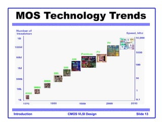
MOS Technology Trends
CMOS VLSI Design
Introduction Slide 14
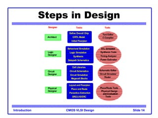
Steps in Design
Define Overall Chip
C/RTL Model
Initial Floorplan
Cell Libraries
Circuit Schematics
Megacell Blocks
Circuit Simulation
Layout and Floorplan
Place and Route
Parasitics Extraction
DRC/LVS/ERC
Behavioral Simulation
Logic Simulation
Synthesis
Datapath Schematics
RTL Simulator
Synthesis Tools
Timing Analyzer
Power Estimator
Text Editor
CCompiler
Schematic Editor
Circuit Simulator
Router
Designer Tasks Tools
Architect
Logic
Designer
Designer
Circuit
Physical
Designer
Place/Route Tools
Physical Design
and Evaluation
Tools
CMOS VLSI Design
Introduction Slide 15
System on a Chip
Source: ARM
CMOS VLSI Design
Introduction Slide 16
Laboratory Exercises
 Layout and evaluation of standard cells
– Familiarity with layout, circuit simulation, timing
 Design and evaluation of an ALU, performance
optimization
– Learn schematic design, timing optimization
 Design, synthesis and analysis of a simple controller as
part of an SoC
– Learn RT-level design, system simulation, logic
synthesis and place-and-route
 If you already have industrial experience with some of
these tools, you can substitute lab for final project
– Need my approval; will expect more from project
CMOS VLSI Design
Introduction Slide 17
Laboratory Design Tools
 We will use commercial CAD tools
– Cadence, Synopsys, etc.
 Commercial software is powerful, but very complex
– Designers sent to long training classes
– Students will benefit from using the software, but
we don’t have the luxury of long training
– TAs have experience with the software
 Start work early in the lab
– Unavailability of workstations is no excuse for late
submissions
– Plan designs carefully and save work frequently
CMOS VLSI Design
Introduction Slide 18
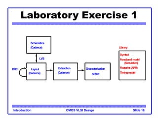
Laboratory Exercise 1
DRC
Schematics
Layout
SPICE
Library
(Simulation)
Functional model
Symbol
Footprint(APR)
Timingmodel
LVS
Extraction
(Cadence) (Cadence)
(Cadence)
Characterization
CMOS VLSI Design
Introduction Slide 19
Laboratory Exercise 2
Library
Library
DRC
LVS
Layout
Schematics
Data PathBlock
Static Timing
Analysis
Layout
Schematic
(Cadence)
Extraction
VerilogXL
Functional
Verification
(Cadence) (Cadence) (Synopsys)
CMOS VLSI Design
Introduction Slide 20
Laboratory Exercise 3
Synthesis
(Synopsis)
Formal
Verification
Control Block
Netlist
Layout
(Synopsys)
Static TimingAnalysis
(Cadence)
APR
(Cadence)
Extraction
(Verplex)
RTLmodel
Verilog
CMOS VLSI Design
Introduction Slide 21
Need for transistors
 Cannot make logic gates with voltage/current source,
RLC components
– Consider steady state behavior of L and C
 Need a “switch”: something where a (small) signal
can control the flow of another signal
CMOS VLSI Design
Introduction Slide 22
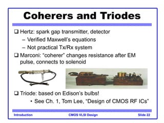
Coherers and Triodes
 Hertz: spark gap transmitter, detector
– Verified Maxwell’s equations
– Not practical Tx/Rx system
 Marconi: “coherer” changes resistance after EM
pulse, connects to solenoid
 Triode: based on Edison’s bulbs!
• See Ch. 1, Tom Lee, “Design of CMOS RF ICs”
CMOS VLSI Design
Introduction Slide 23
A Brief History of MOS
Some of the events which led to the
microprocessor
Photographs from “State of the Art: A photographic
history of the integrated circuit,” Augarten, Ticknor &
Fields, 1983.
They can also be viewed on the Smithsonian web site,
http://smithsonianchips.si.edu/
CMOS VLSI Design
Introduction Slide 24
Lilienfeld patents
1930: “Method and
apparatus for controlling
electric currents”, U.S.
Patent 1,745,175
1933: “Device for controlling
electric current”, U. S. Patent
1,900,018
CMOS VLSI Design
Introduction Slide 25
Bell Labs
 1940: Ohl develops the PN Junction
 1945: Shockley's laboratory established
 1947: Bardeen and Brattain create point contact
transistor (U.S. Patent 2,524,035)
Diagram from patent application
CMOS VLSI Design
Introduction Slide 26
Bell Labs
 1951: Shockley develops a junction transistor
manufacturable in quantity (U.S. Patent 2,623,105)
Diagram from patent application
CMOS VLSI Design
Introduction Slide 27
1950s – Silicon Valley
 1950s: Shockley in Silicon Valley
 1955: Noyce joins Shockley Laboratories
 1954: The first transistor radio
 1957: Noyce leaves Shockley Labs to form Fairchild with
Jean Hoerni and Gordon Moore
 1958: Hoerni invents technique for diffusing impurities into Si
to build planar transistors using a SiO2 insulator
 1959: Noyce develops first true IC using planar transistors,
back-to-back PN junctions for isolation, diode-isolated Si
resistors and SiO2 insulation with evaporated metal wiring on
top
CMOS VLSI Design
Introduction Slide 28
The Integrated Circuit
 1959: Jack Kilby, working at TI, dreams up the
idea of a monolithic “integrated circuit”
– Components connected by hand-soldered
wires and isolated by “shaping”, PN-diodes
used as resistors (U.S. Patent 3,138,743)
Diagram from patent application
CMOS VLSI Design
Introduction Slide 29
Integrated Circuits
 1961: TI and Fairchild introduce the first logic
ICs ($50 in quantity)
 1962: RCA develops the first MOS transistor
RCA 16-transistor MOSFET IC
Fairchild bipolar RTL Flip-Flop
CMOS VLSI Design
Introduction Slide 30
Computer-Aided Design
 1967: Fairchild develops the “Micromosaic” IC using
CAD
– Final Al layer of interconnect could be customized for
different applications
 1968: Noyce, Moore leave Fairchild, start Intel
CMOS VLSI Design
Introduction Slide 31
RAMs
 1970: Fairchild introduces 256-bit Static RAMs
 1970: Intel starts selling1K-bit Dynamic RAMs
Fairchild 4100 256-bit SRAM Intel 1103 1K-bit DRAM
CMOS VLSI Design
Introduction Slide 32
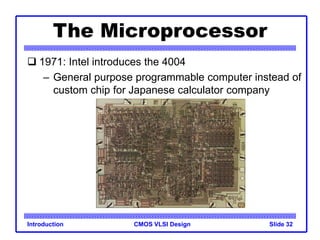
The Microprocessor
 1971: Intel introduces the 4004
– General purpose programmable computer instead of
custom chip for Japanese calculator company

lec0Intro.ppt

  • 1.
    CMOS VLSI Design IntroductionSlide 1 Introduction to CMOS VLSI Design Adnan Aziz The University of Texas at Austin
  • 2.
    CMOS VLSI Design IntroductionSlide 2 Organization  Prerequisites: logic design, basic computer organization – See sample questions  Architecture design versus chip design – Example: innovative processor  Overview of material – Bottom-up approach, CAD tools – See syllabus for individual topics  Course organization – Website, TA, office hours, HW, projects  Acknowledgements – J. Abraham (UT), D. Harris (HMC), R. Tupuri (AMD)
  • 3.
    CMOS VLSI Design IntroductionSlide 3 Course relevance  2007 world wide sales of chips: ~250B$ – Primarily digital – High-margin business – Basis for systems  Most CE graduates work in – VLSI design: Intel, Qualcomm – System design: HP, Cisco – Software: Microsoft, Google
  • 4.
    CMOS VLSI Design IntroductionSlide 4 Systems and Chips  This course: designing ICs – Part of a system: chips + board + software + … – System companies: HP, Cisco – Chip companies: Intel, Qualcomm – nVidia vs. Hercules  Example: high-end data switch – Marketing gives range of specs, architect tries to meet them – Off the shelf chips, embedded software – Why don’t we teach system design?
  • 5.
    CMOS VLSI Design IntroductionSlide 5 Course Goals  Learn to design and analyze state-of-the-art digital VLSI chips using CMOS technology  Employ hierarchical design methods – Understand design issues at the layout, transistor, logic and register-transfer levels – Use integrated circuit cells as building blocks – Use commercial design software in the lab  Understand the complete design flow – Won’t cover architecture, solid-state physics, analog design – Superficial treatment of transistor functioning
  • 6.
    CMOS VLSI Design IntroductionSlide 6 Course Information  Instructor: Adnan Aziz – (512) 465-9774, Adnan@ece.utexas.edu – http://www.ece.utexas.edu/~adnan  Course Web Page – Link from my page  Book: Weste and Harris, CMOS VLSI Design: A Circuits and Systems Perspective, AW, 3rd edition
  • 7.
    CMOS VLSI Design IntroductionSlide 7 Work in the Course  Lectures: largely from text (not always in sequence)  Homework: roughly 6 HWs – Relatively straightforward review questions  Laboratory exercises – Three major exercises dealing with various aspects of VLSI design – Complete each section before the deadline  Grad students: VLSI design project – Design an IP core, architecture to layout Course involves a large amount of work throughout the semester
  • 8.
    CMOS VLSI Design IntroductionSlide 8 What Will We Cover?  Designing chips containing lots of transistors – How basic components work (transistors, gates, flops, memories, adders, – Complexity management: hierarchy and CAD tools  Key issues: – Creating logical structures from transistors – Performance analysis and optimization – Testing: functional and manufacturing – Power consumption, clocking, I/O, etc.
  • 9.
    CMOS VLSI Design IntroductionSlide 9 Exams and Grading  Two midterm tests: in class, open book/notes; samples will be posted – Dates for exams in syllabus – Final: exam (360R), project (382M)  Lab dates in syllabus – Bonus/penalty for early/late submission  Weights for homework, exams, project are in syllabus – Relative weights of MT1/2, Lab 1/2/3 intentionally not specified
  • 10.
    CMOS VLSI Design IntroductionSlide 10 Academic Honesty  Cheating will not be tolerated – OK to discuss homework, laboratory exercises with classmates, TAs and the instructors – However: write the homework and lab exercises by yourself  We check for cheating, and report incidents
  • 11.
    CMOS VLSI Design IntroductionSlide 11 General Principles  Technology changes fast => important to understand general principles – optimization, tradeoffs – work as part of a group – leverage existing work: programs ,building blocks  Concepts remain the same: – Example: relays -> tubes -> bipolar transistors -> MOS transistors
  • 12.
    CMOS VLSI Design IntroductionSlide 12 Types of IC Designs  IC Designs can be Analog or Digital  Digital designs can be one of three groups  Full Custom – Every transistor designed and laid out by hand  ASIC (Application-Specific Integrated Circuits) – Designs synthesized automatically from a high-level language description  Semi-Custom – Mixture of custom and synthesized modules
  • 13.
    CMOS VLSI Design IntroductionSlide 13 MOS Technology Trends
  • 14.
    CMOS VLSI Design IntroductionSlide 14 Steps in Design Define Overall Chip C/RTL Model Initial Floorplan Cell Libraries Circuit Schematics Megacell Blocks Circuit Simulation Layout and Floorplan Place and Route Parasitics Extraction DRC/LVS/ERC Behavioral Simulation Logic Simulation Synthesis Datapath Schematics RTL Simulator Synthesis Tools Timing Analyzer Power Estimator Text Editor CCompiler Schematic Editor Circuit Simulator Router Designer Tasks Tools Architect Logic Designer Designer Circuit Physical Designer Place/Route Tools Physical Design and Evaluation Tools
  • 15.
    CMOS VLSI Design IntroductionSlide 15 System on a Chip Source: ARM
  • 16.
    CMOS VLSI Design IntroductionSlide 16 Laboratory Exercises  Layout and evaluation of standard cells – Familiarity with layout, circuit simulation, timing  Design and evaluation of an ALU, performance optimization – Learn schematic design, timing optimization  Design, synthesis and analysis of a simple controller as part of an SoC – Learn RT-level design, system simulation, logic synthesis and place-and-route  If you already have industrial experience with some of these tools, you can substitute lab for final project – Need my approval; will expect more from project
  • 17.
    CMOS VLSI Design IntroductionSlide 17 Laboratory Design Tools  We will use commercial CAD tools – Cadence, Synopsys, etc.  Commercial software is powerful, but very complex – Designers sent to long training classes – Students will benefit from using the software, but we don’t have the luxury of long training – TAs have experience with the software  Start work early in the lab – Unavailability of workstations is no excuse for late submissions – Plan designs carefully and save work frequently
  • 18.
    CMOS VLSI Design IntroductionSlide 18 Laboratory Exercise 1 DRC Schematics Layout SPICE Library (Simulation) Functional model Symbol Footprint(APR) Timingmodel LVS Extraction (Cadence) (Cadence) (Cadence) Characterization
  • 19.
    CMOS VLSI Design IntroductionSlide 19 Laboratory Exercise 2 Library Library DRC LVS Layout Schematics Data PathBlock Static Timing Analysis Layout Schematic (Cadence) Extraction VerilogXL Functional Verification (Cadence) (Cadence) (Synopsys)
  • 20.
    CMOS VLSI Design IntroductionSlide 20 Laboratory Exercise 3 Synthesis (Synopsis) Formal Verification Control Block Netlist Layout (Synopsys) Static TimingAnalysis (Cadence) APR (Cadence) Extraction (Verplex) RTLmodel Verilog
  • 21.
    CMOS VLSI Design IntroductionSlide 21 Need for transistors  Cannot make logic gates with voltage/current source, RLC components – Consider steady state behavior of L and C  Need a “switch”: something where a (small) signal can control the flow of another signal
  • 22.
    CMOS VLSI Design IntroductionSlide 22 Coherers and Triodes  Hertz: spark gap transmitter, detector – Verified Maxwell’s equations – Not practical Tx/Rx system  Marconi: “coherer” changes resistance after EM pulse, connects to solenoid  Triode: based on Edison’s bulbs! • See Ch. 1, Tom Lee, “Design of CMOS RF ICs”
  • 23.
    CMOS VLSI Design IntroductionSlide 23 A Brief History of MOS Some of the events which led to the microprocessor Photographs from “State of the Art: A photographic history of the integrated circuit,” Augarten, Ticknor & Fields, 1983. They can also be viewed on the Smithsonian web site, http://smithsonianchips.si.edu/
  • 24.
    CMOS VLSI Design IntroductionSlide 24 Lilienfeld patents 1930: “Method and apparatus for controlling electric currents”, U.S. Patent 1,745,175 1933: “Device for controlling electric current”, U. S. Patent 1,900,018
  • 25.
    CMOS VLSI Design IntroductionSlide 25 Bell Labs  1940: Ohl develops the PN Junction  1945: Shockley's laboratory established  1947: Bardeen and Brattain create point contact transistor (U.S. Patent 2,524,035) Diagram from patent application
  • 26.
    CMOS VLSI Design IntroductionSlide 26 Bell Labs  1951: Shockley develops a junction transistor manufacturable in quantity (U.S. Patent 2,623,105) Diagram from patent application
  • 27.
    CMOS VLSI Design IntroductionSlide 27 1950s – Silicon Valley  1950s: Shockley in Silicon Valley  1955: Noyce joins Shockley Laboratories  1954: The first transistor radio  1957: Noyce leaves Shockley Labs to form Fairchild with Jean Hoerni and Gordon Moore  1958: Hoerni invents technique for diffusing impurities into Si to build planar transistors using a SiO2 insulator  1959: Noyce develops first true IC using planar transistors, back-to-back PN junctions for isolation, diode-isolated Si resistors and SiO2 insulation with evaporated metal wiring on top
  • 28.
    CMOS VLSI Design IntroductionSlide 28 The Integrated Circuit  1959: Jack Kilby, working at TI, dreams up the idea of a monolithic “integrated circuit” – Components connected by hand-soldered wires and isolated by “shaping”, PN-diodes used as resistors (U.S. Patent 3,138,743) Diagram from patent application
  • 29.
    CMOS VLSI Design IntroductionSlide 29 Integrated Circuits  1961: TI and Fairchild introduce the first logic ICs ($50 in quantity)  1962: RCA develops the first MOS transistor RCA 16-transistor MOSFET IC Fairchild bipolar RTL Flip-Flop
  • 30.
    CMOS VLSI Design IntroductionSlide 30 Computer-Aided Design  1967: Fairchild develops the “Micromosaic” IC using CAD – Final Al layer of interconnect could be customized for different applications  1968: Noyce, Moore leave Fairchild, start Intel
  • 31.
    CMOS VLSI Design IntroductionSlide 31 RAMs  1970: Fairchild introduces 256-bit Static RAMs  1970: Intel starts selling1K-bit Dynamic RAMs Fairchild 4100 256-bit SRAM Intel 1103 1K-bit DRAM
  • 32.
    CMOS VLSI Design IntroductionSlide 32 The Microprocessor  1971: Intel introduces the 4004 – General purpose programmable computer instead of custom chip for Japanese calculator company