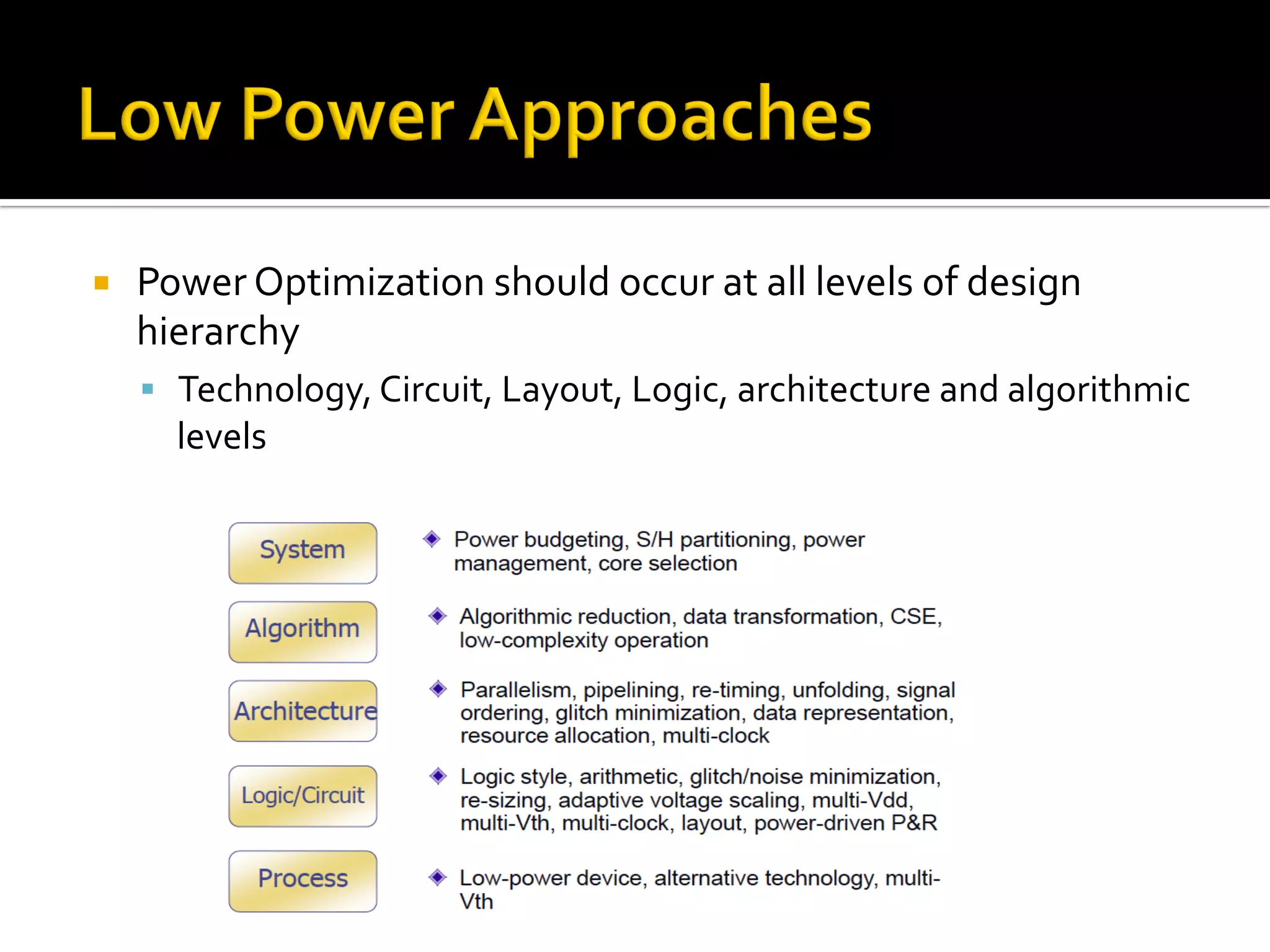
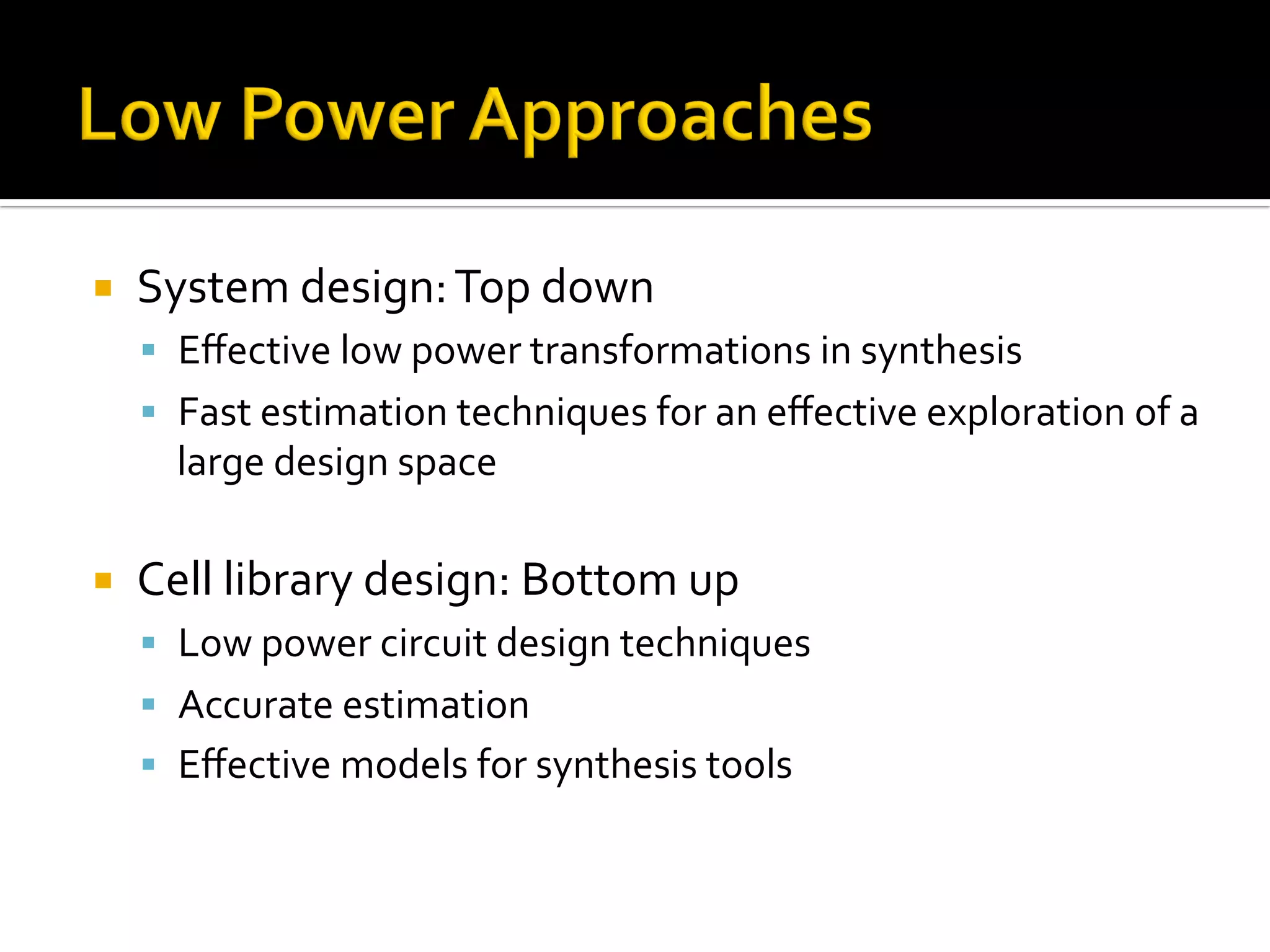
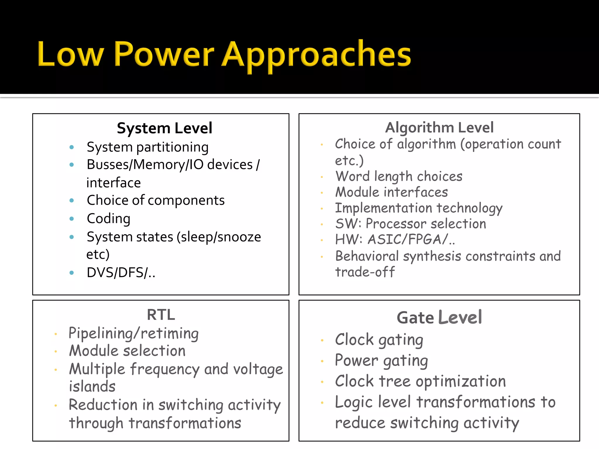
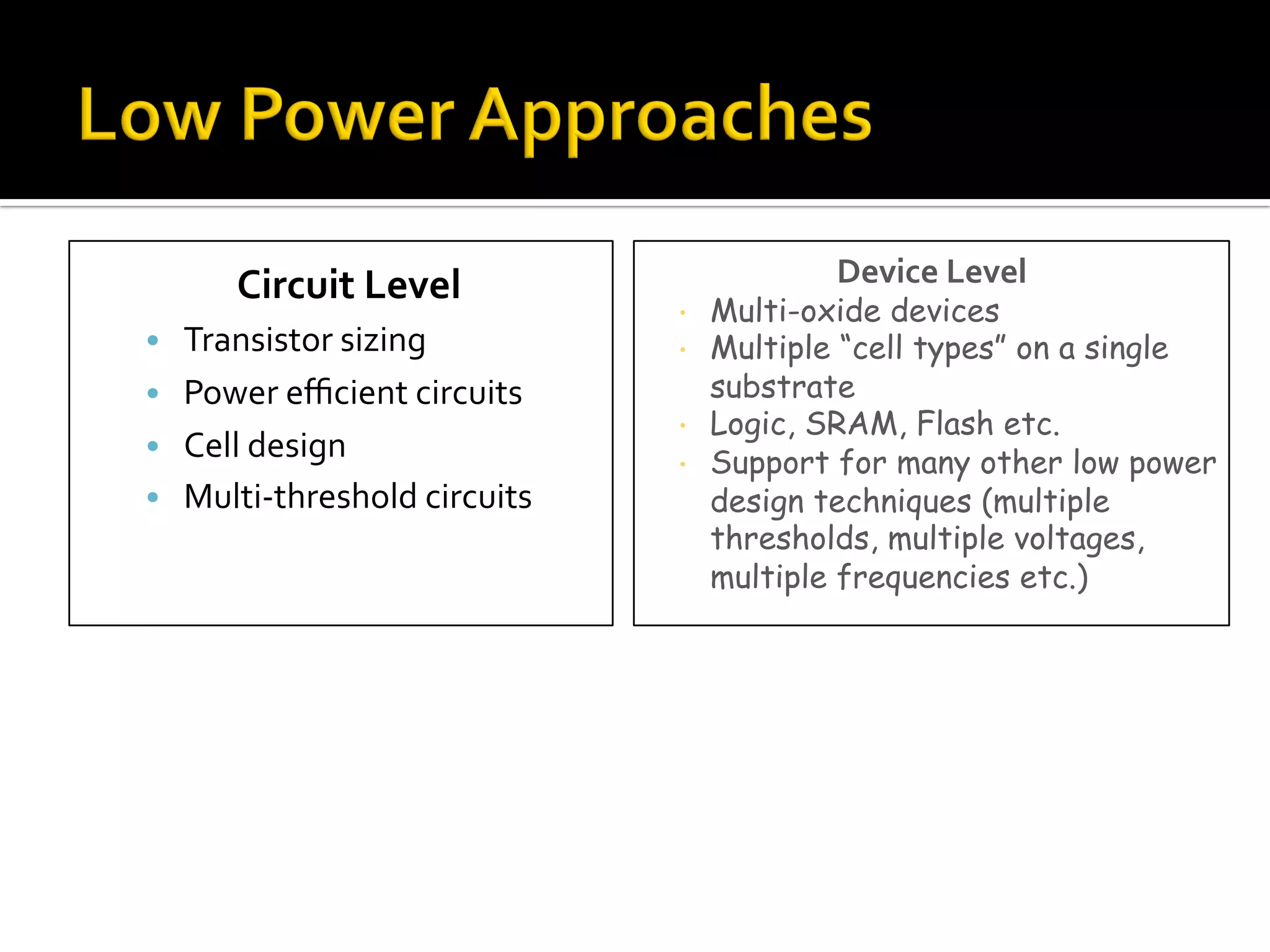
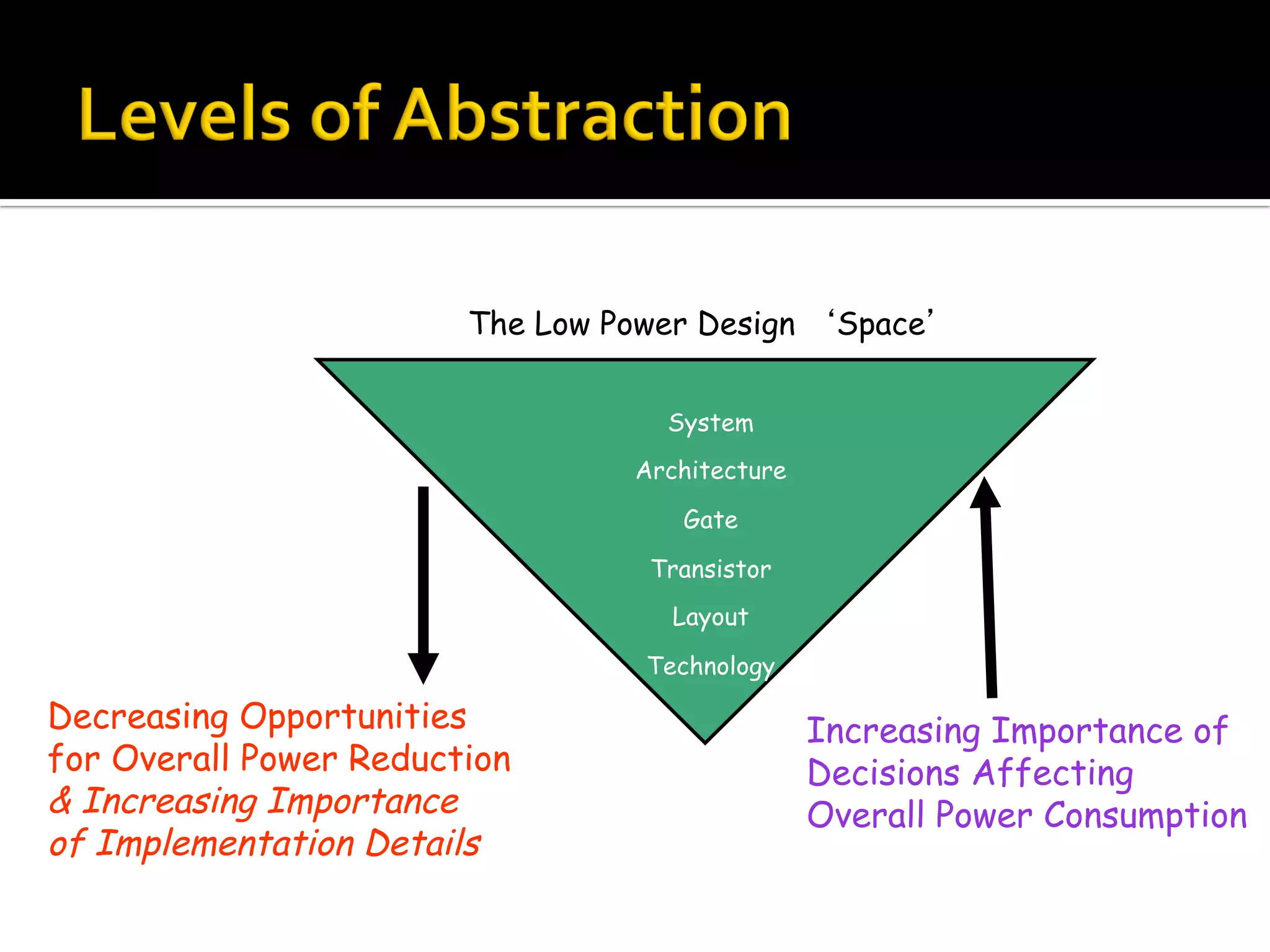
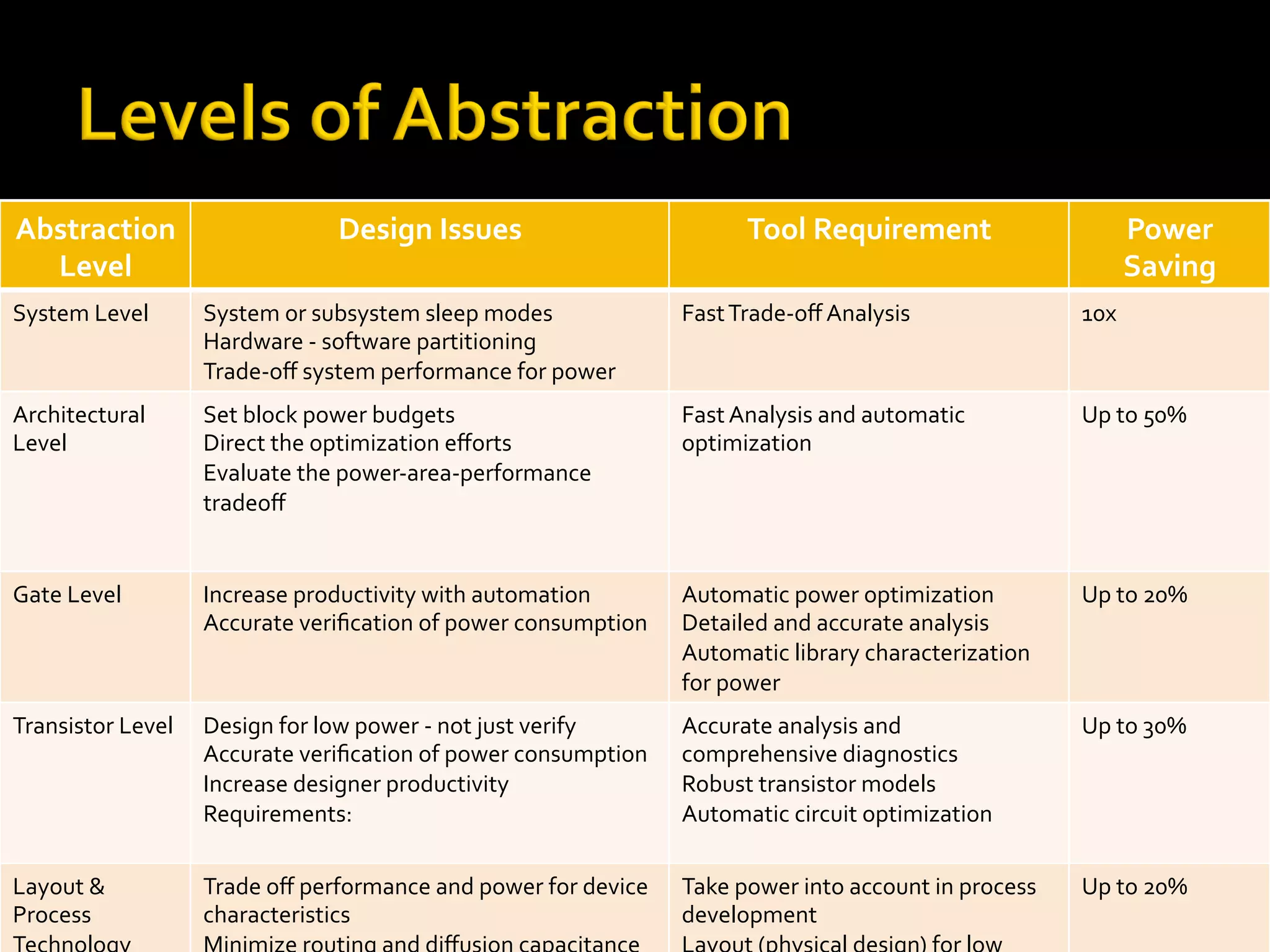
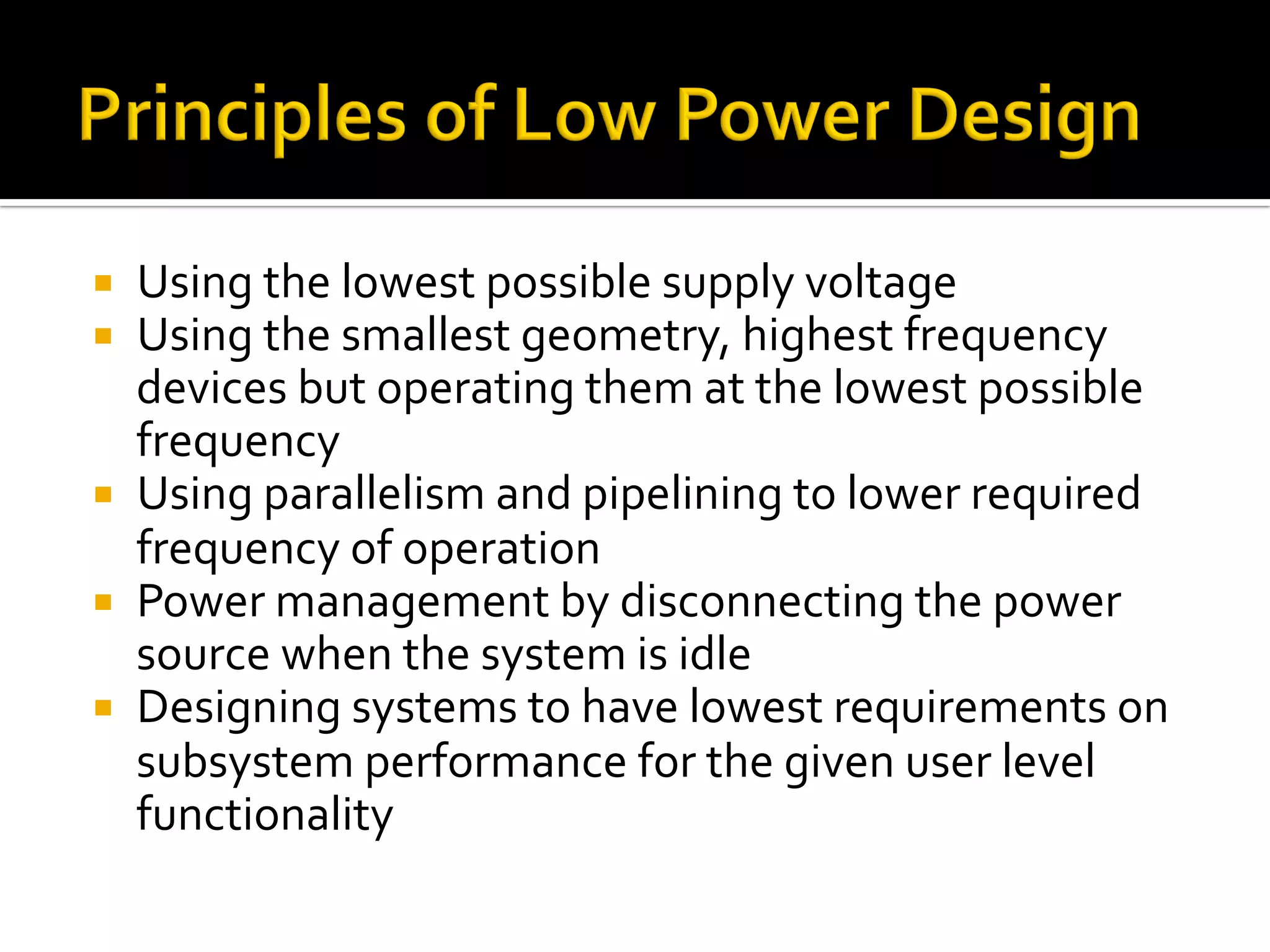
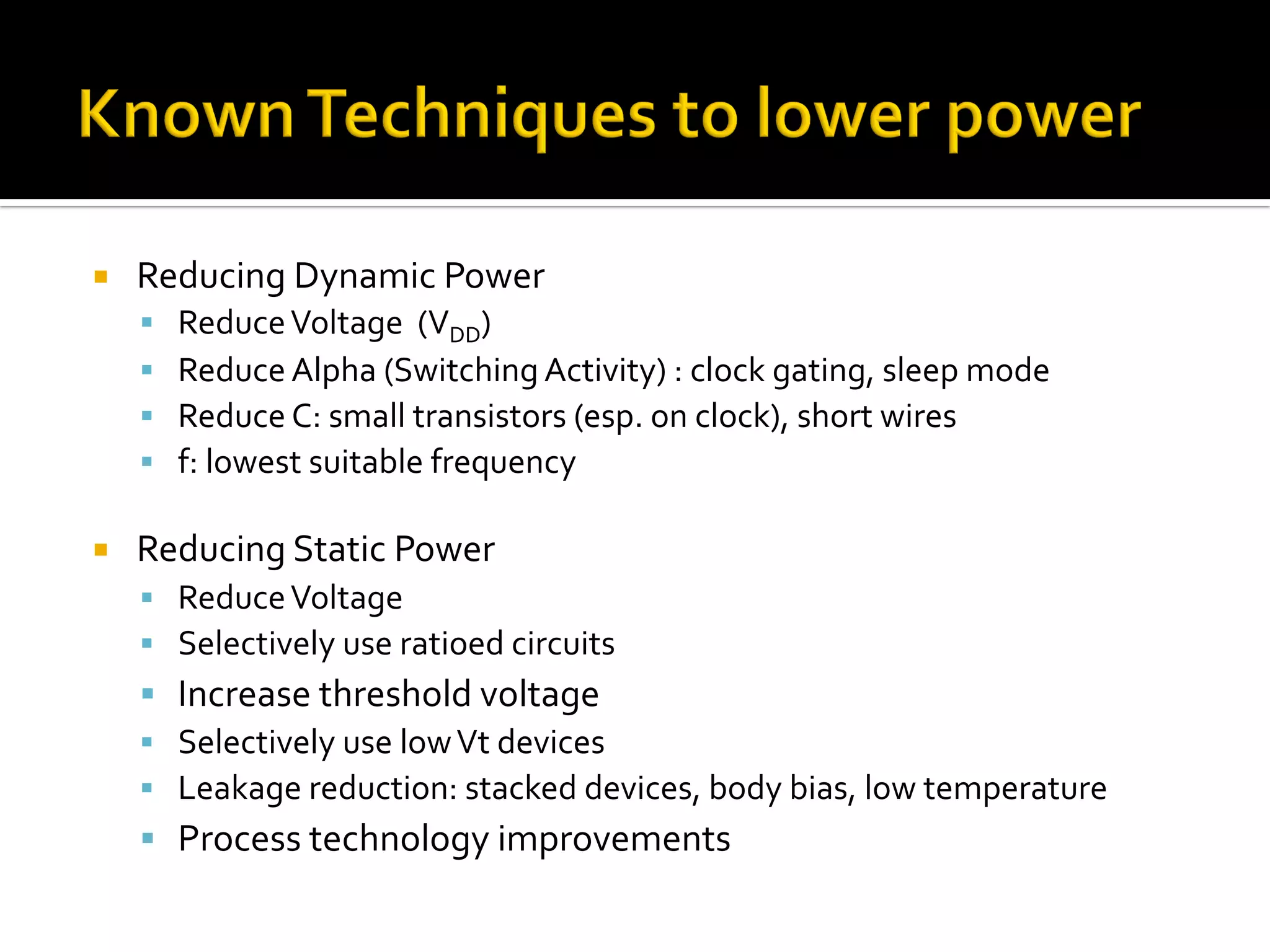
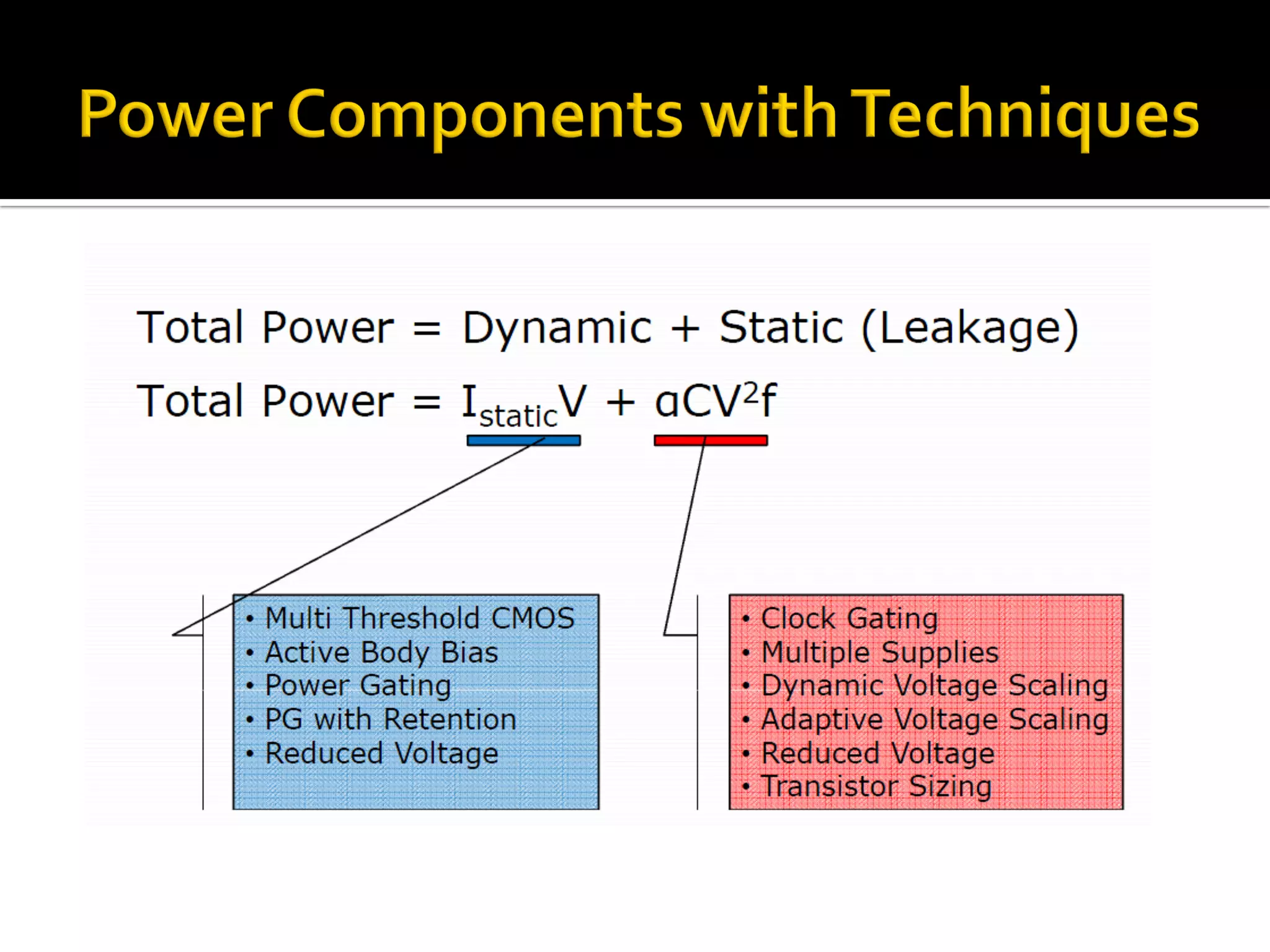
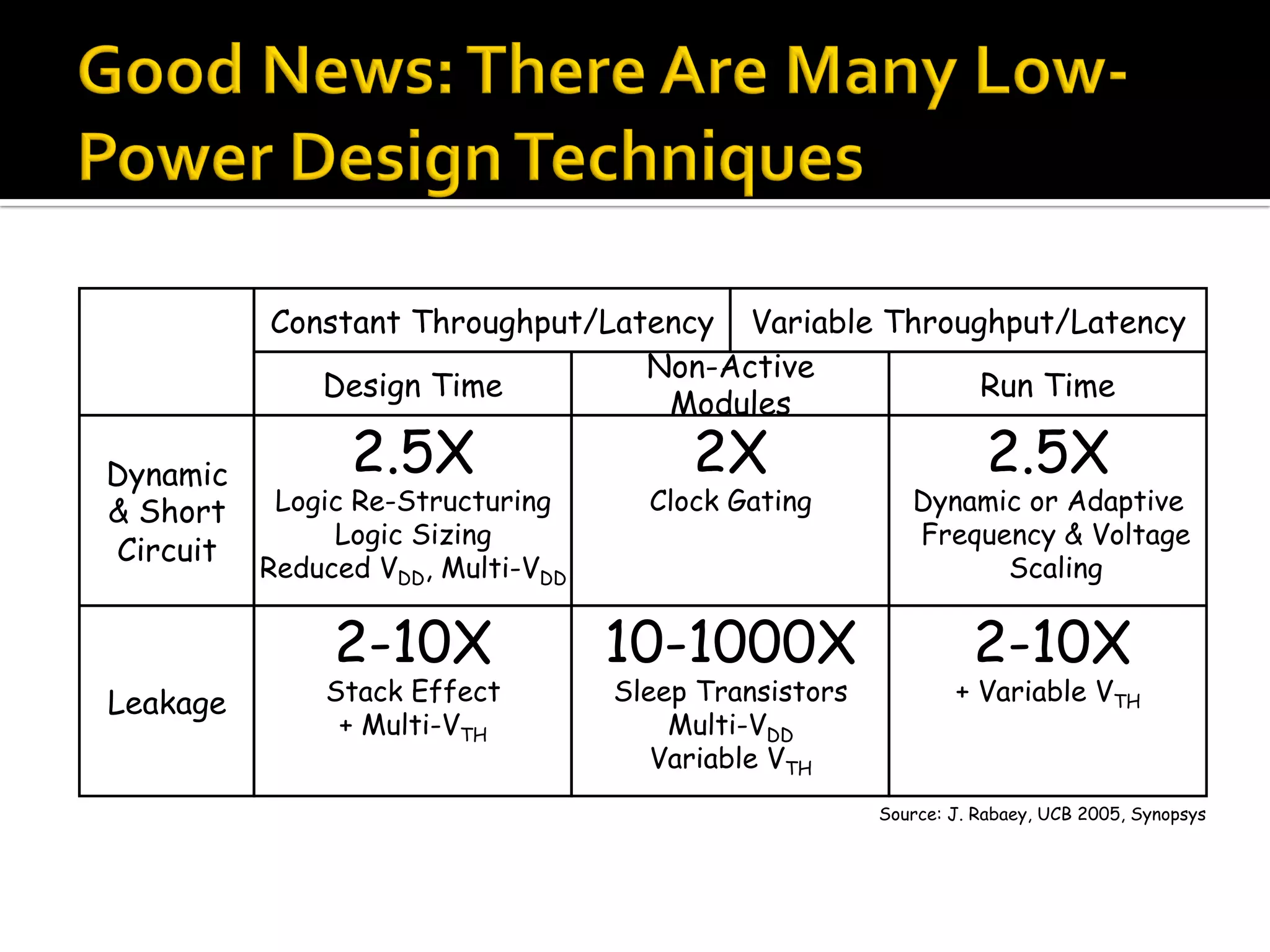
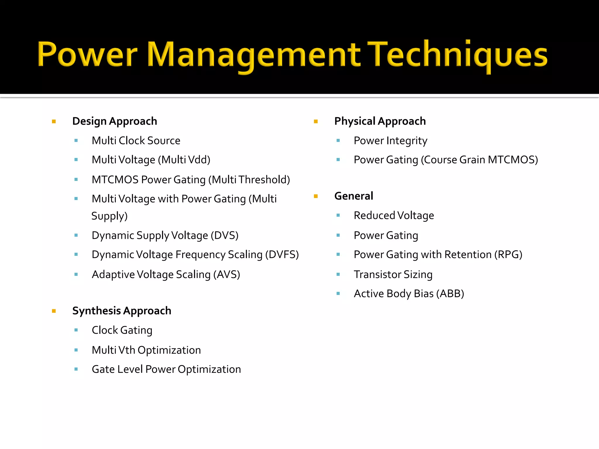
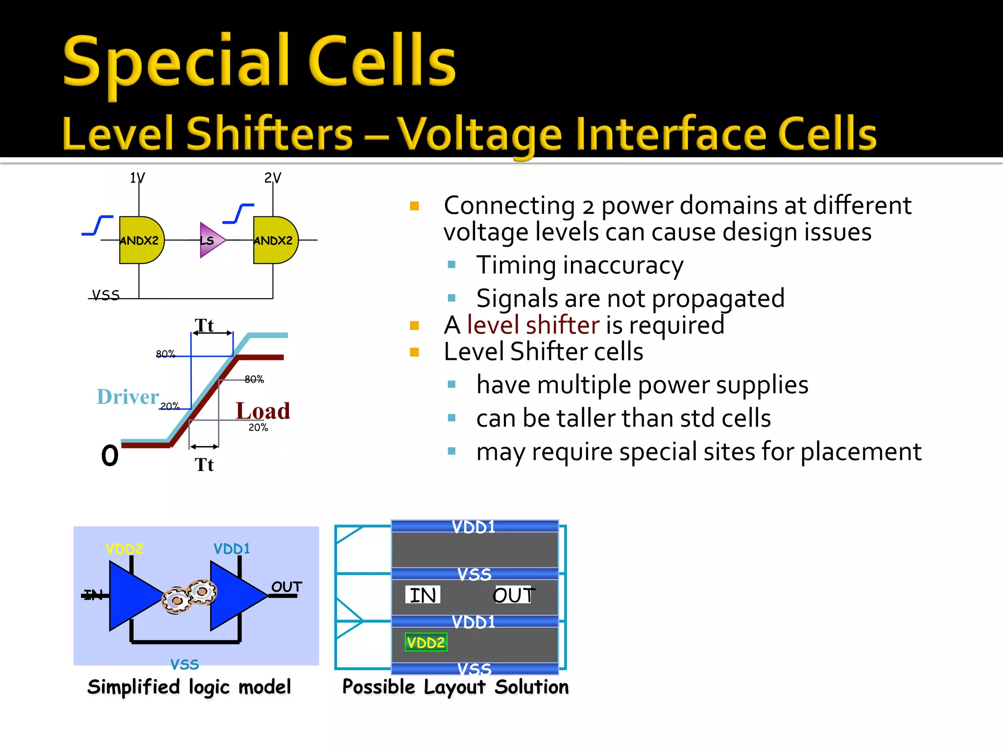
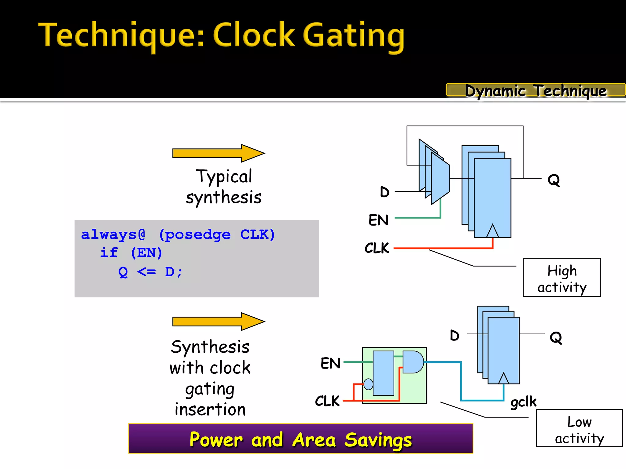
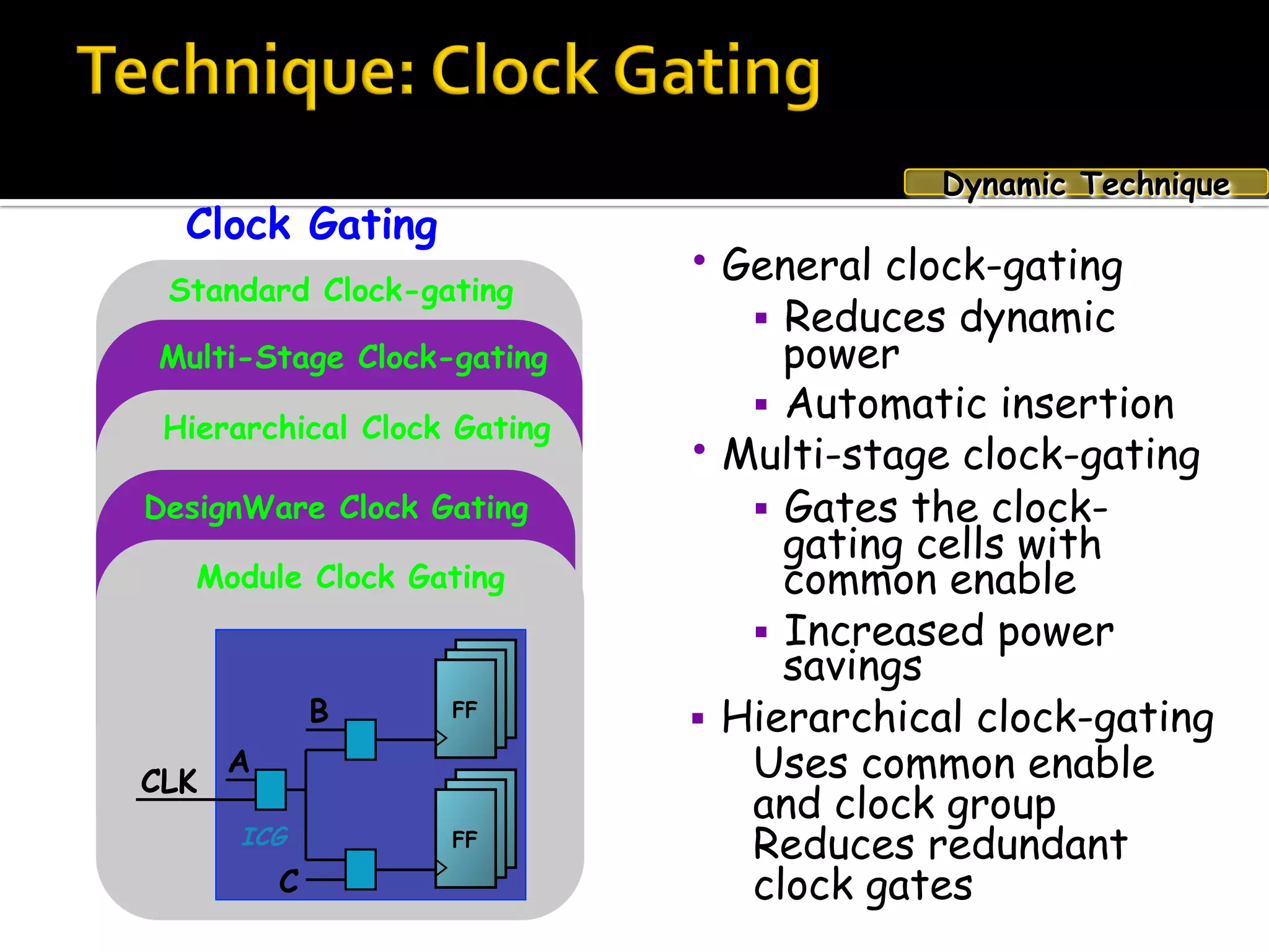
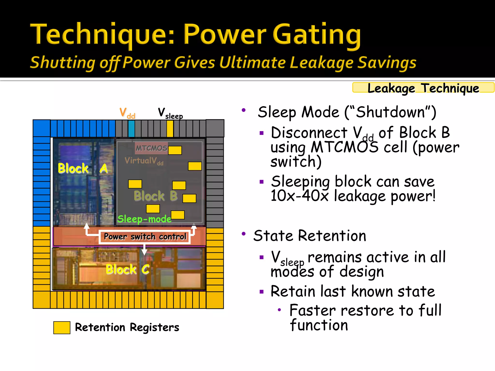
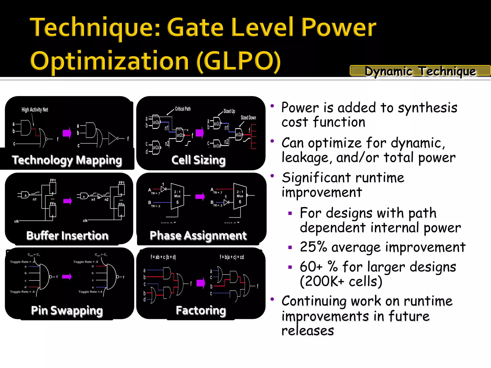
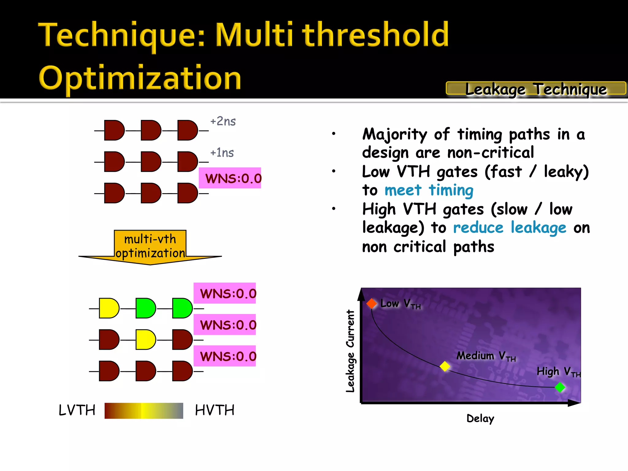
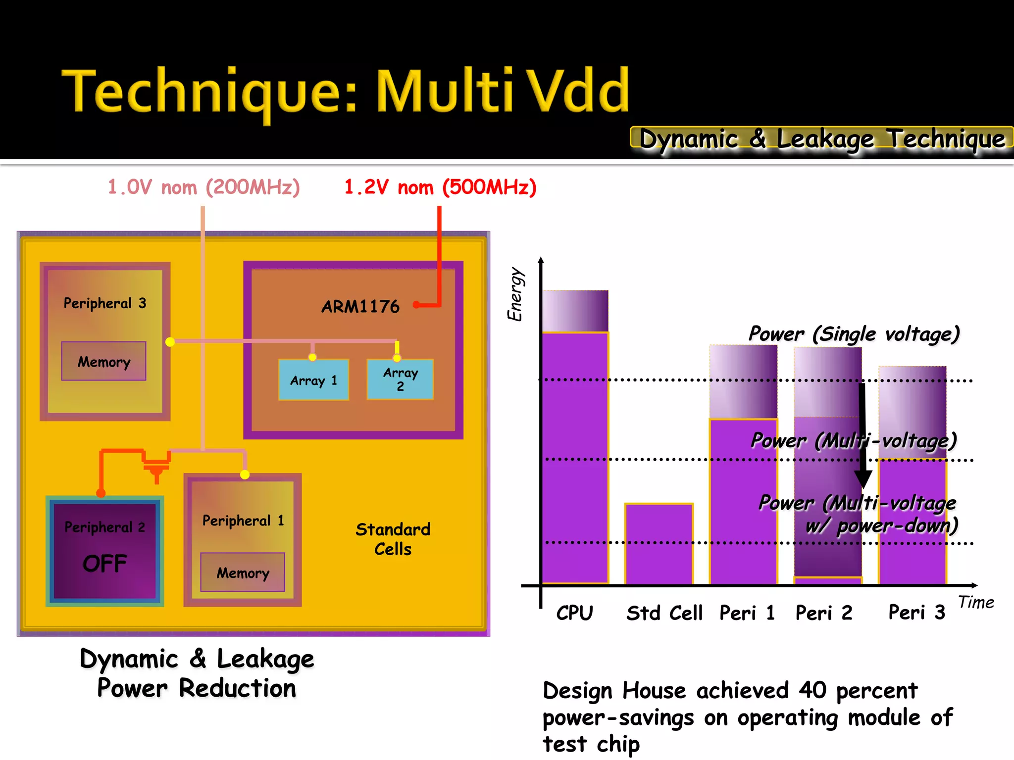
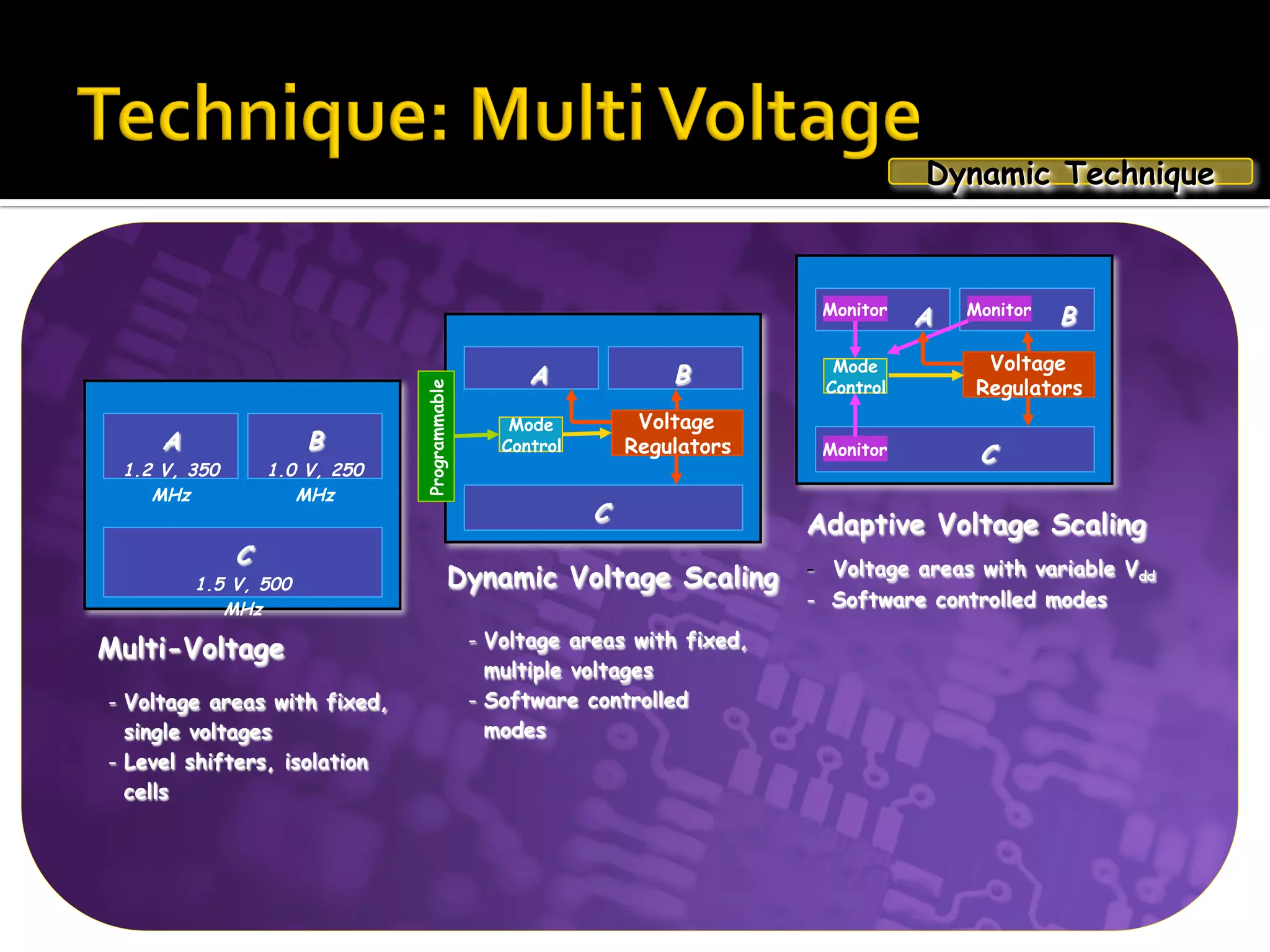
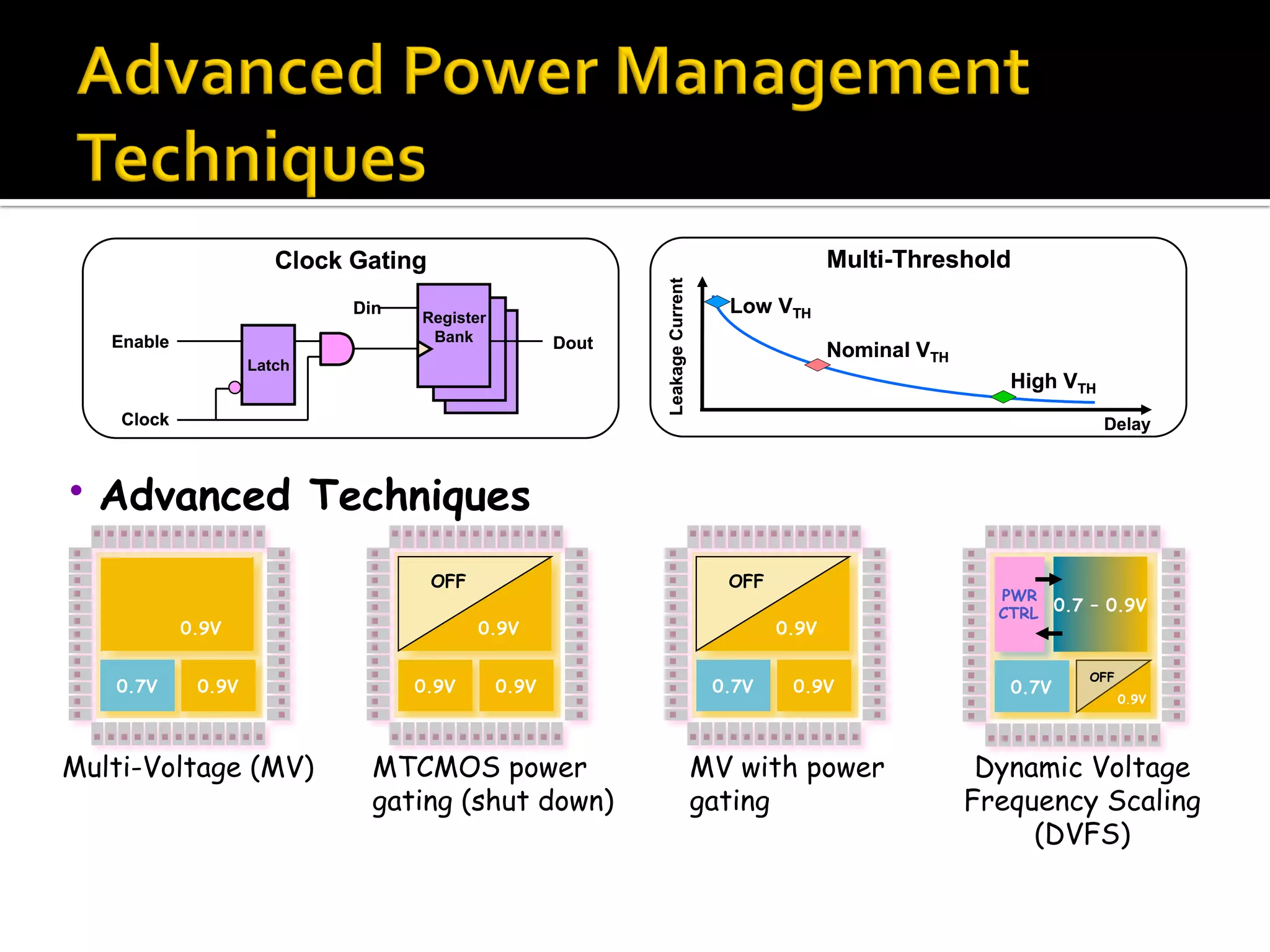
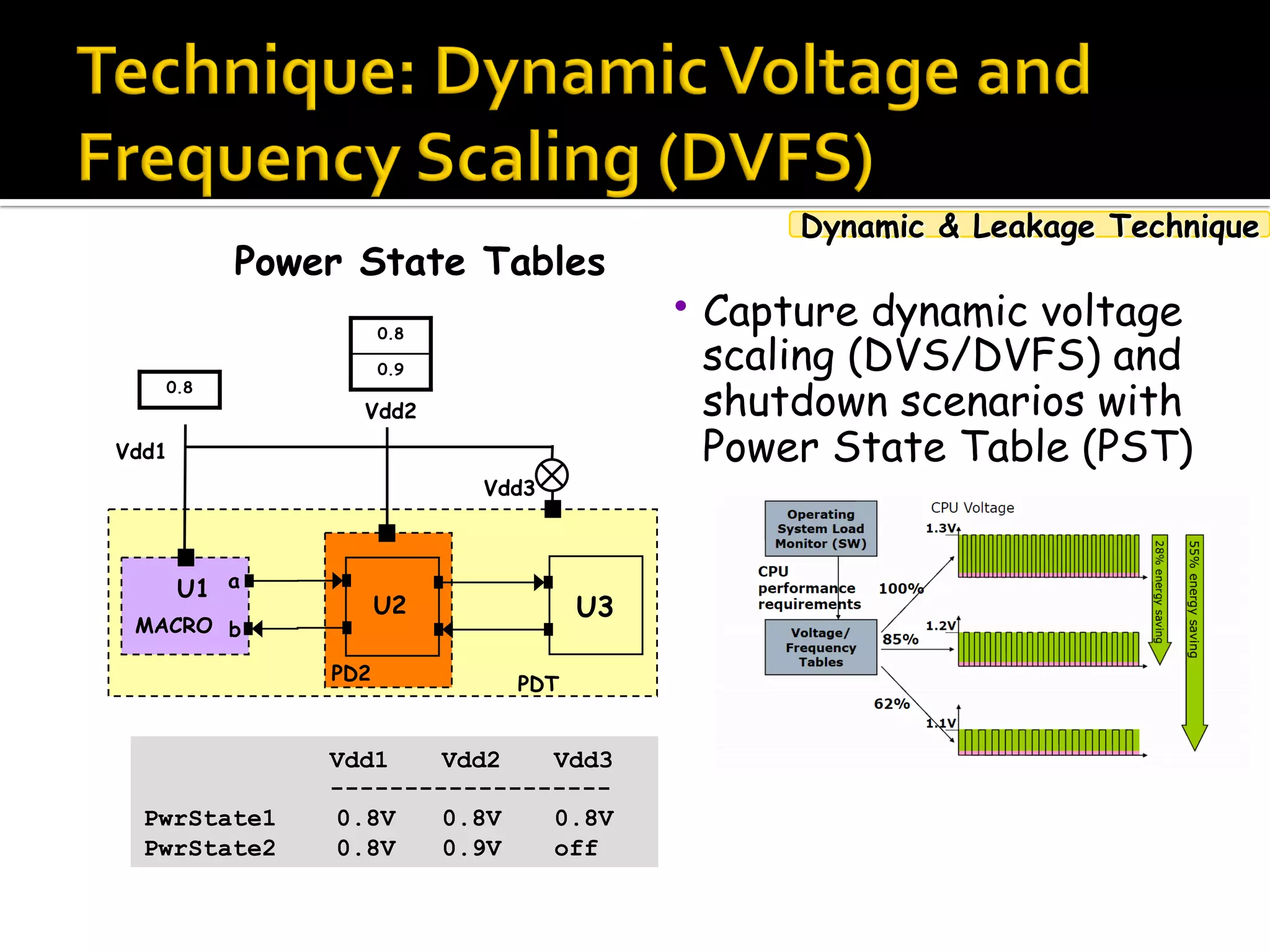
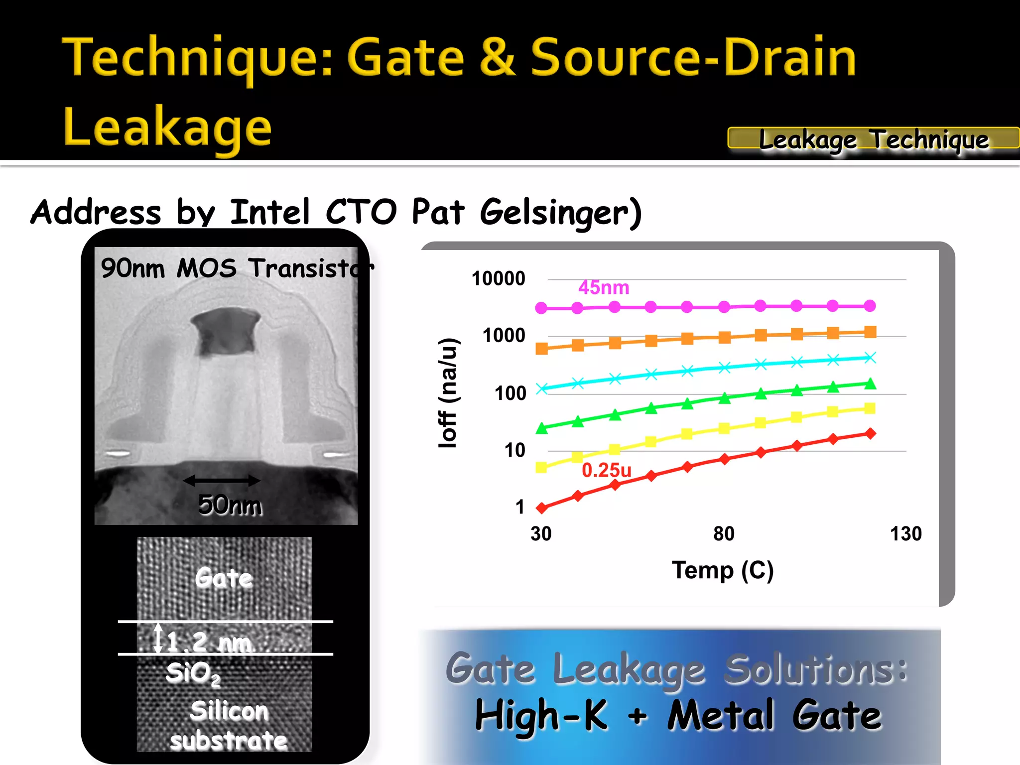
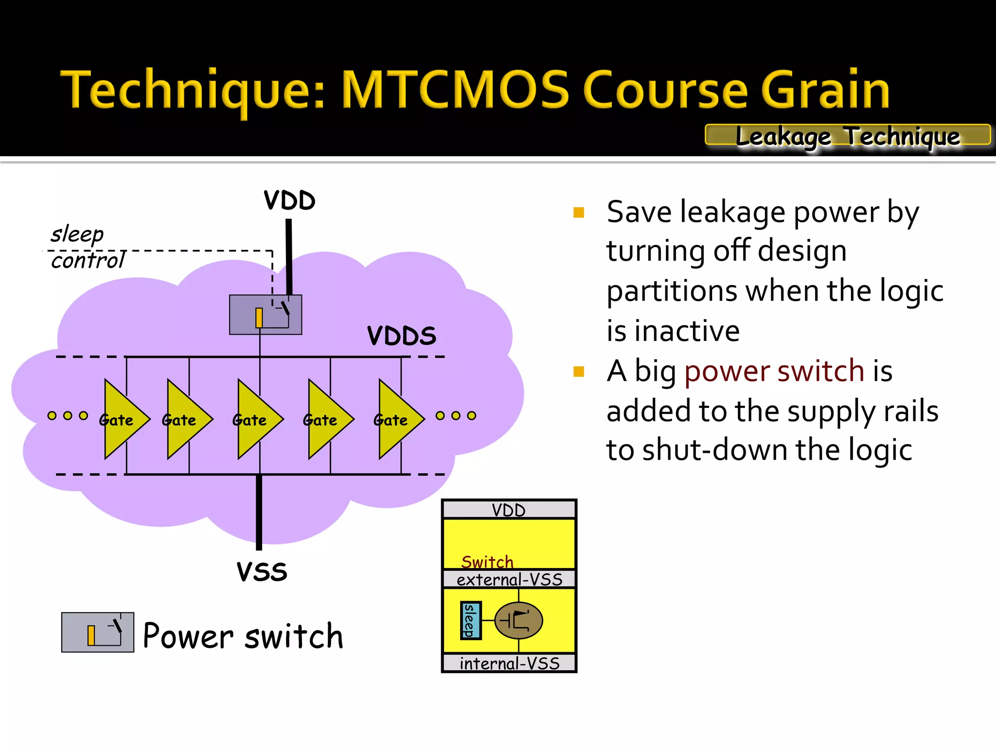
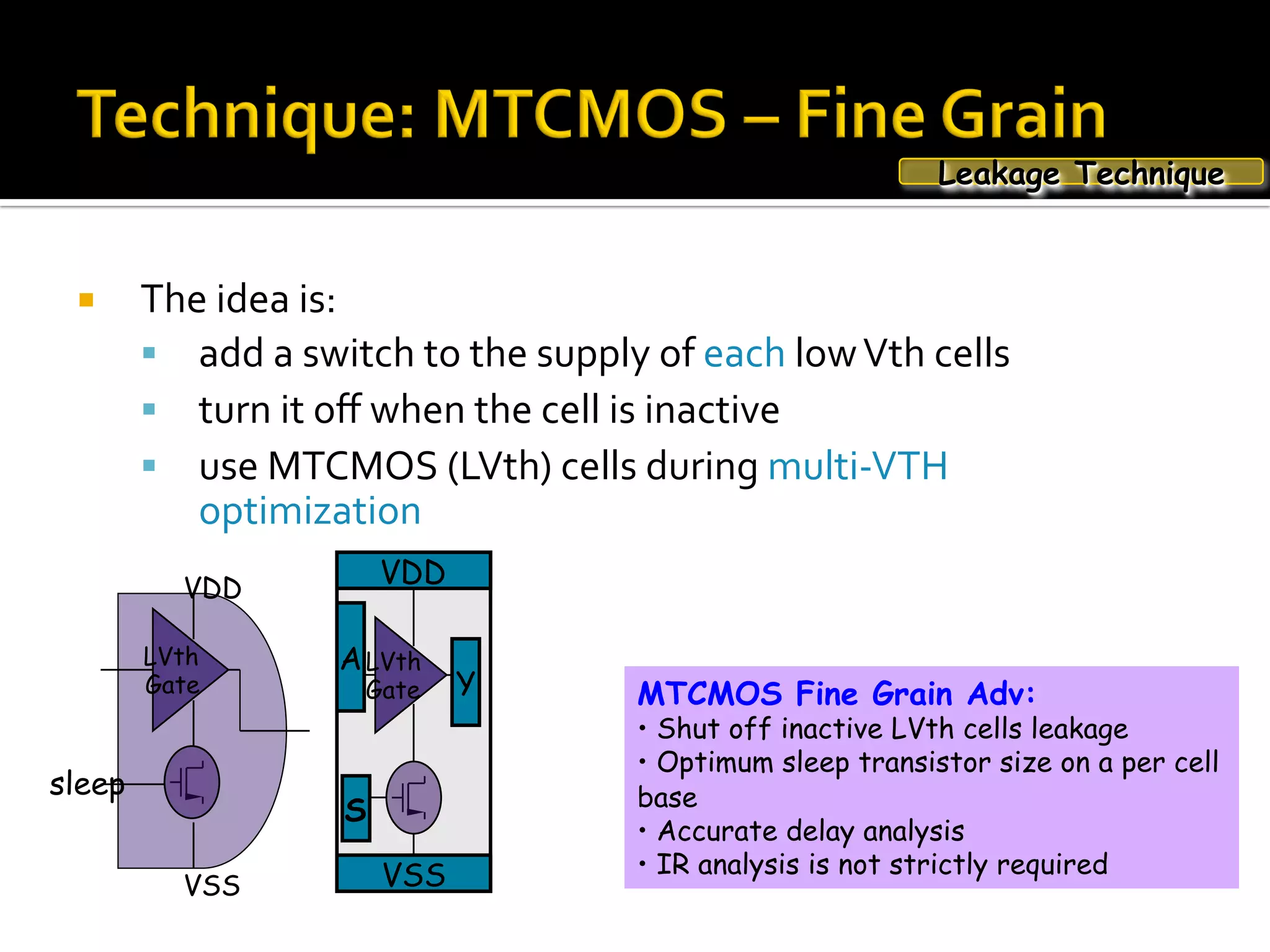
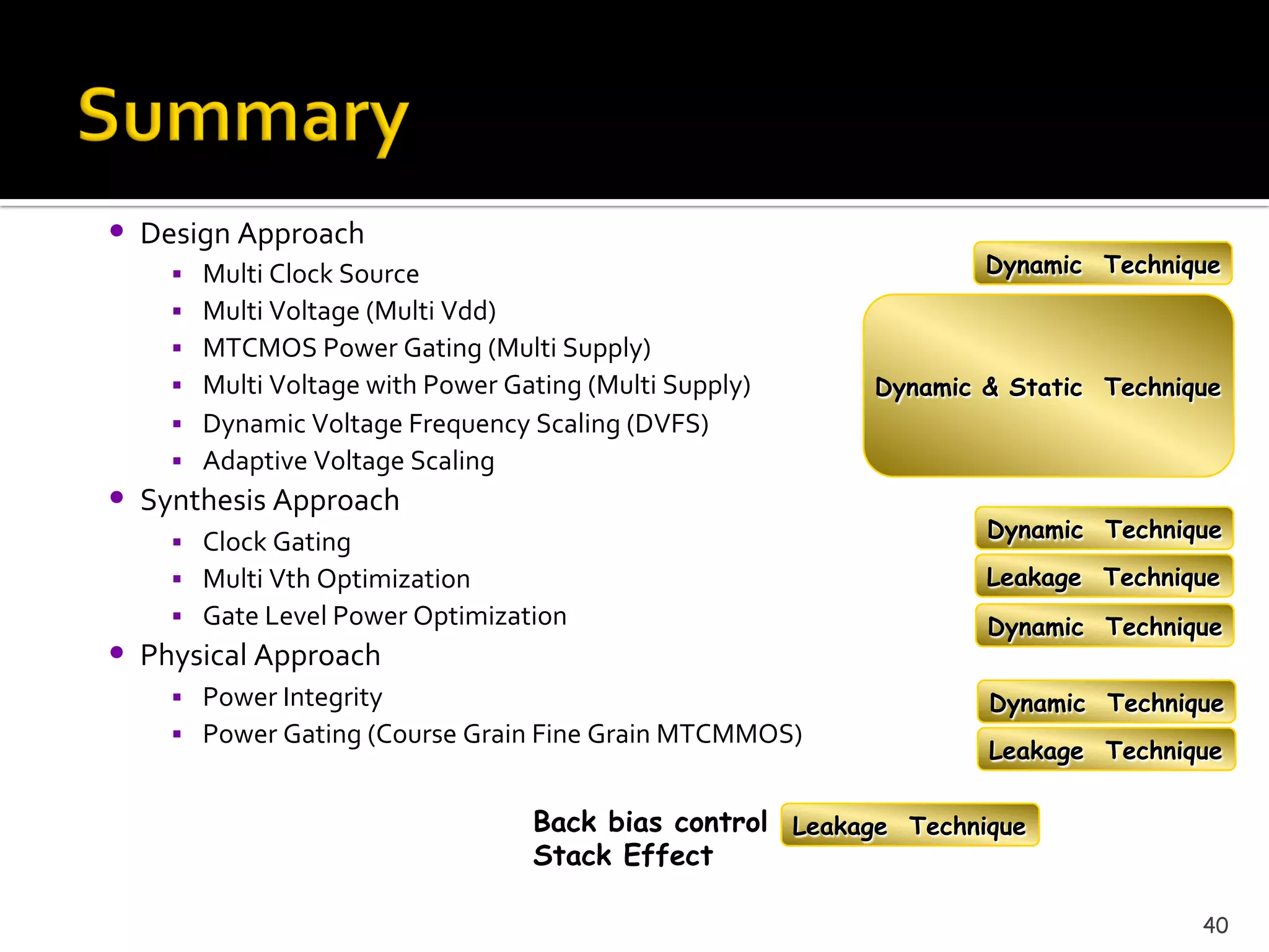
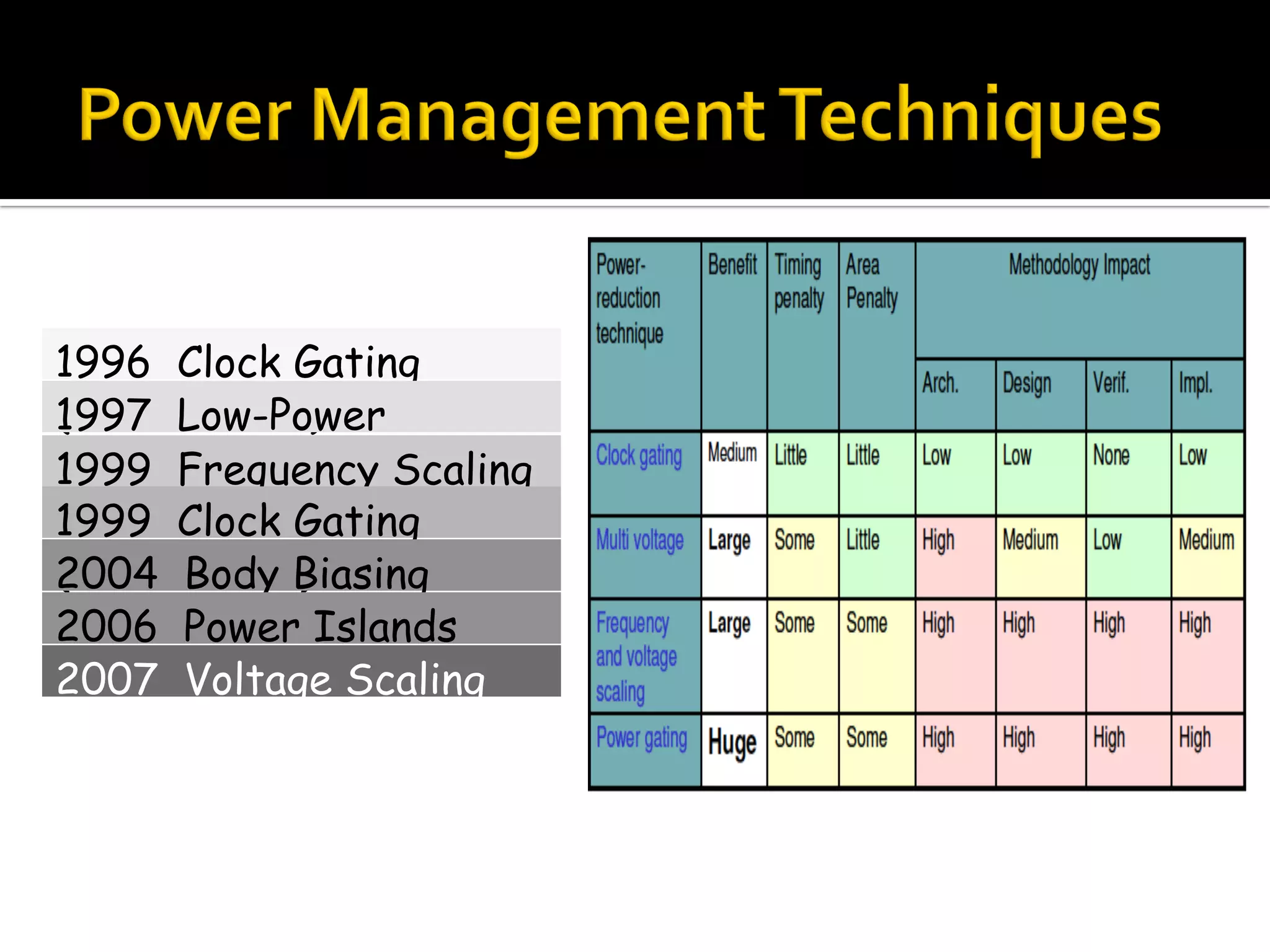
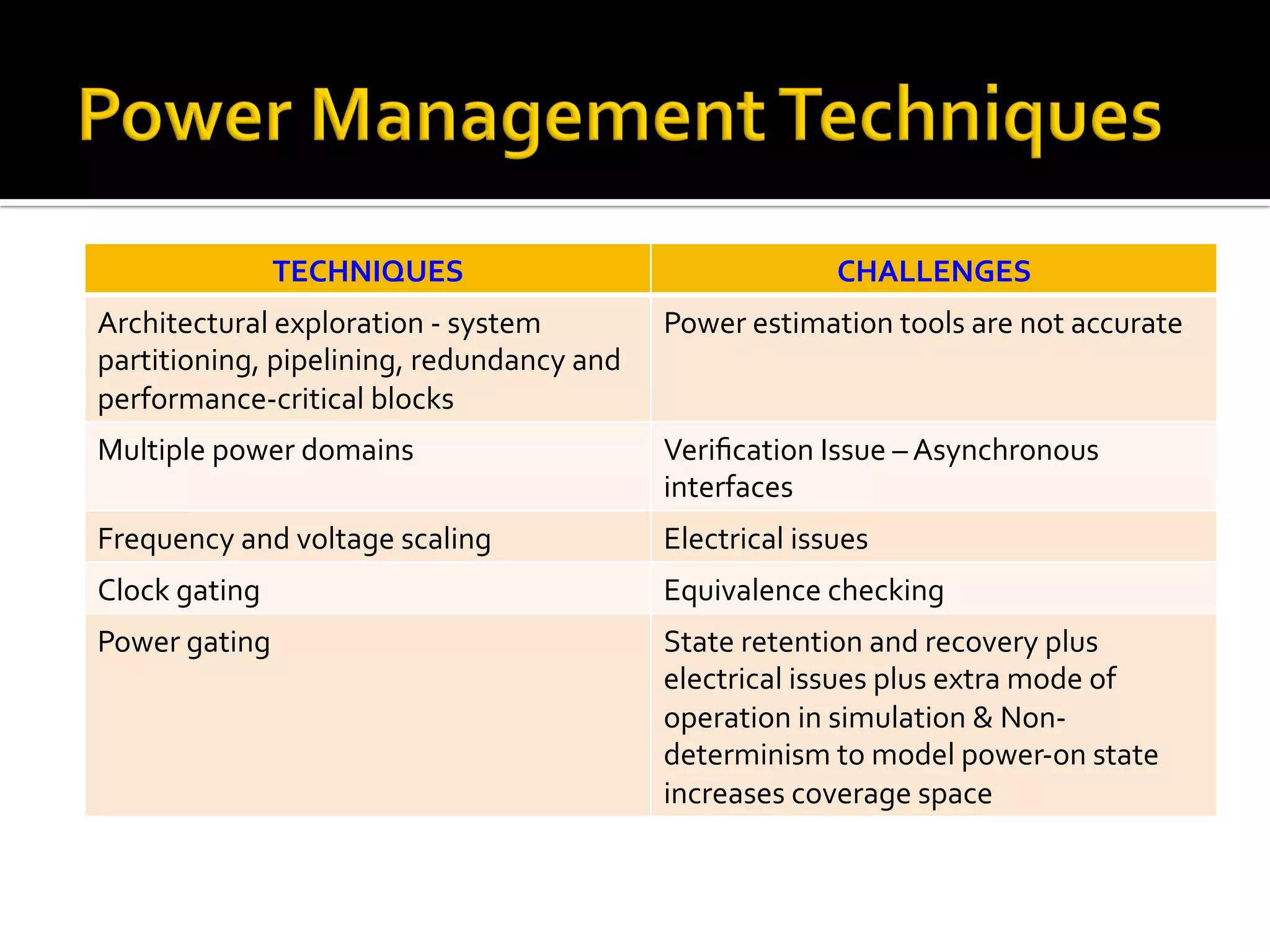
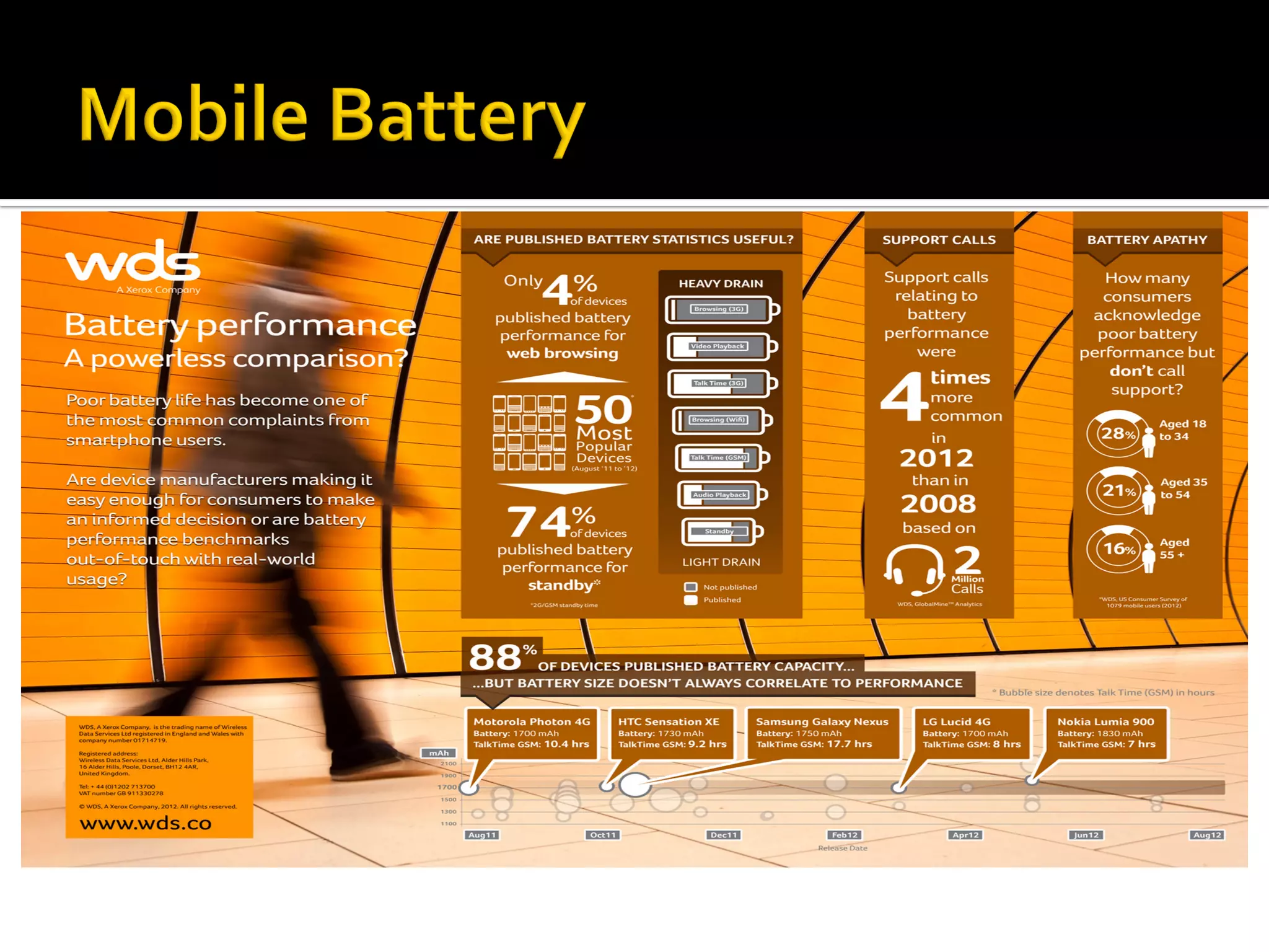
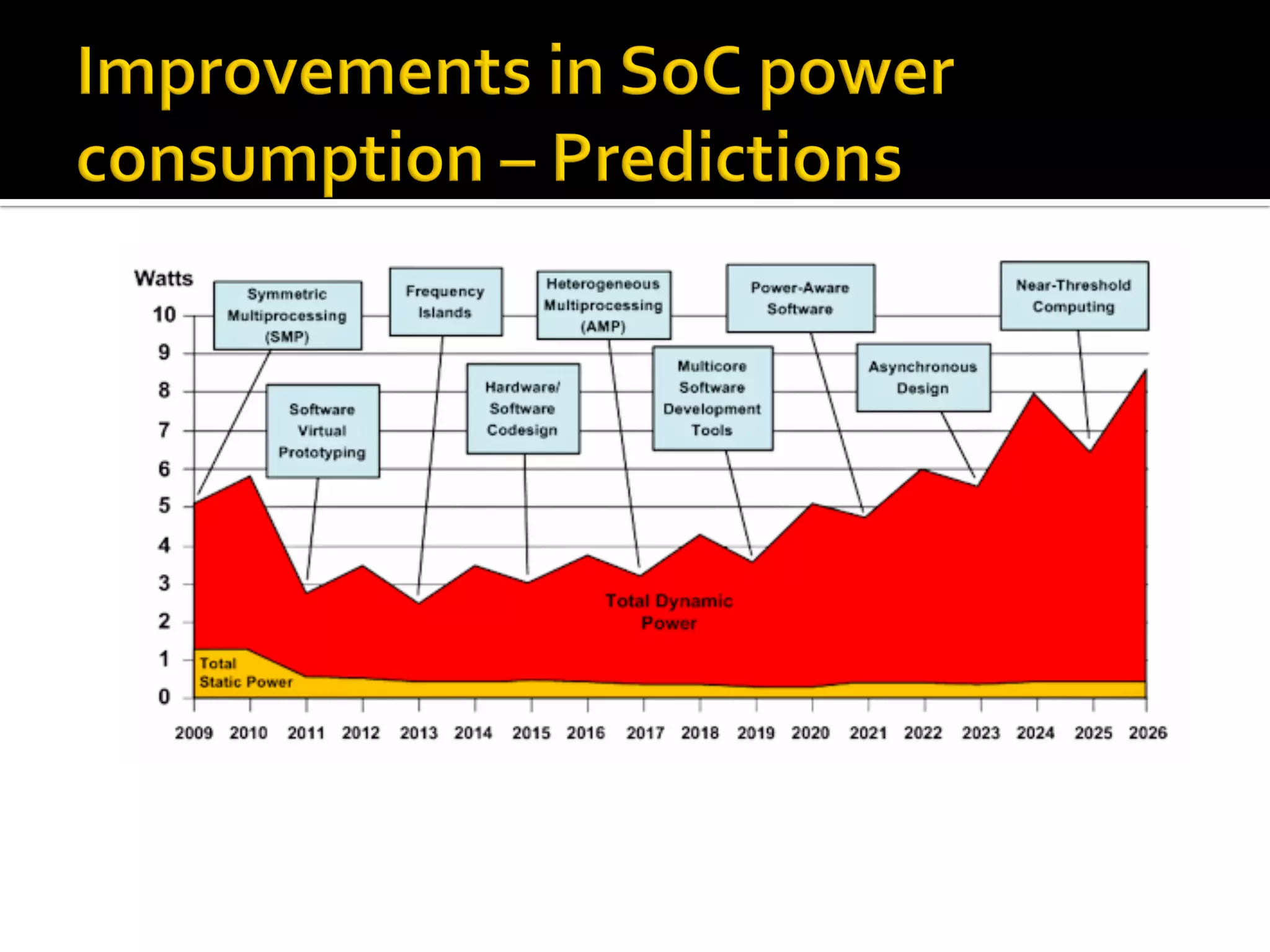
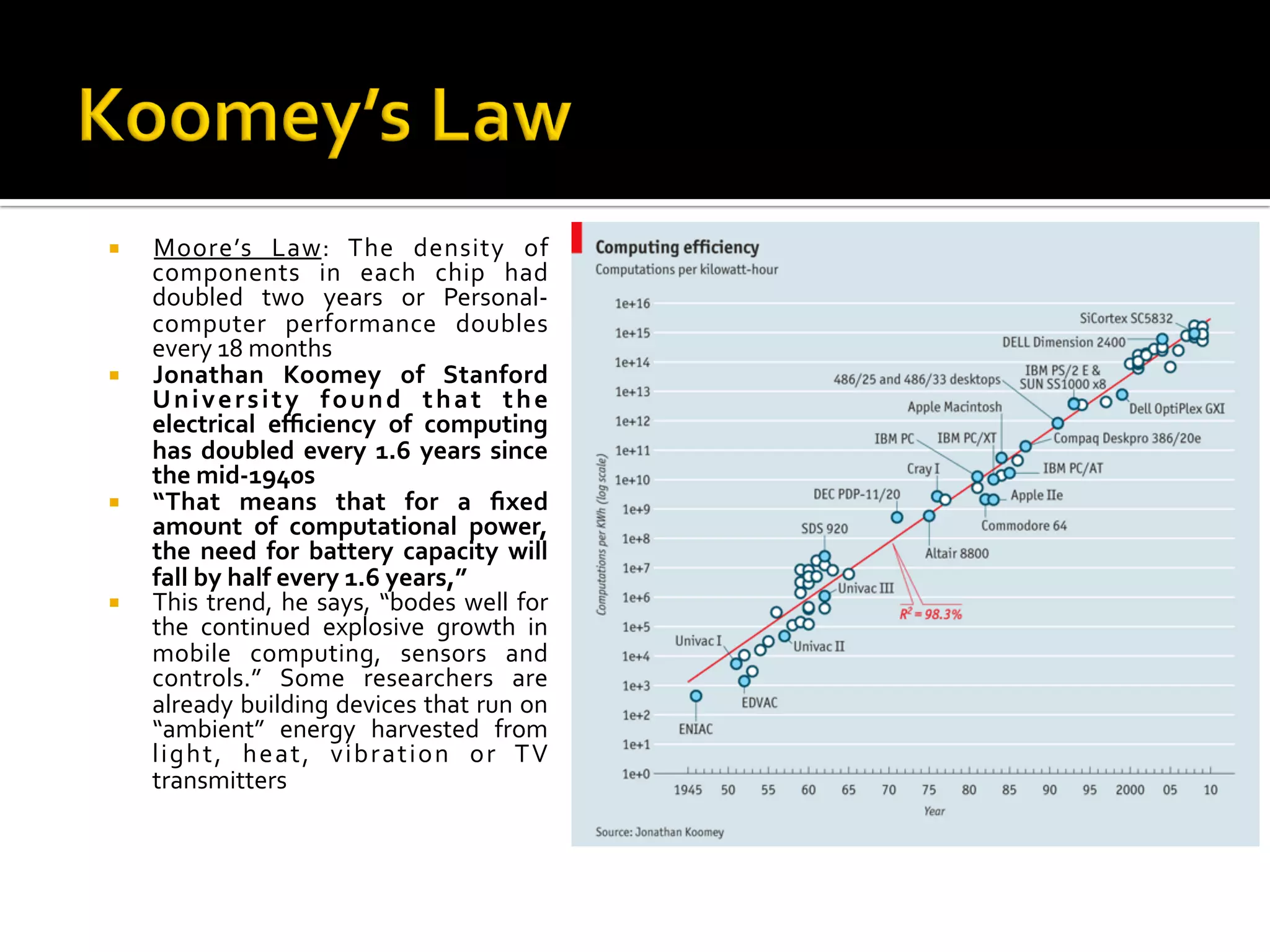
5. • Power forced the technology change to CMOS in the 80’s
• Today, there is no alternative to CMOS
1950 1960 1970 1980 1990 2000 2010
0
14
12
10
8
6
4
2
Vacuum IBM 360
IBM 370 IBM 3033
Fujitsu M380
IBM 3081
IBM 4381
CDC Cyber 205
IBM 3090
Fujitsu M-780
IBM 3090S
NTT
Fujitsu VP2000
IBM ES9000
IBM RY4
IBM RY6
IBM RY5
IBM RY7
IBM GP
Pulsar
Apache
Merced
Pentium II(DSIP)
Mckinley
T-Rex
Pentium 4
Year of Announcement
Bipolar
CMOS
Source: Roger Schmidt, IBM Corp
ModuleHeatFlux(Watts/cm2)
Squadrons
Prescott
Jayhawk
Requirement
6.
7. ¡ Portability: Battery life,
Increased functionality
and Heat generation
¡ Huge server farms
¡ Environmental awareness
Our world is mobile and connected!
The image cannot be displayed. Your computer may not have enough memory to open the image, or the image may have been
corrupted. Restart your computer, and then open the file again. If the red x still appears, you may have to delete the image and
then insert it again.
Design for Low Power is the solution
8. ¡ E n e r g y e ffi c i e n t
infrastructure
¡ To deliver more functionality
in the same footprint
¡ G a i n s f r o m p r o c e s s
migration diminishing, what
can be done as the demand
for performance continues
to increase?
11. ¡ Low power design techniques
§ Effectiveness
§ Effect/tradeoff with other design parameters like
area (cost), performance, reliability,
manufacturability etc.
¡ Power modeling and estimation
§ Accuracy of the models
§ Time for estimation
14. System Level
• System partitioning
• Busses/Memory/IO devices /
interface
• Choice of components
• Coding
• System states (sleep/snooze
etc)
• DVS/DFS/..
Algorithm Level
• Choice of algorithm (operation count
etc.)
• Word length choices
• Module interfaces
• Implementation technology
• SW: Processor selection
• HW: ASIC/FPGA/..
• Behavioral synthesis constraints and
trade-off
RTL
• Pipelining/retiming
• Module selection
• Multiple frequency and voltage
islands
• Reduction in switching activity
through transformations
Gate Level
• Clock gating
• Power gating
• Clock tree optimization
• Logic level transformations to
reduce switching activity
15. Circuit Level
• Transistor sizing
• Power efficient circuits
• Cell design
• Multi-threshold circuits
Device Level
• Multi-oxide devices
• Multiple “cell types” on a single
substrate
• Logic, SRAM, Flash etc.
• Support for many other low power
design techniques (multiple
thresholds, multiple voltages,
multiple frequencies etc.)
17. Abstraction
Level
Design Issues
Tool Requirement Power
Saving
System Level System or subsystem sleep modes
Hardware - software partitioning
Trade-off system performance for power
Fast Trade-off Analysis 10x
Architectural
Level
Set block power budgets
Direct the optimization efforts
Evaluate the power-area-performance
tradeoff
Fast Analysis and automatic
optimization
Up to 50%
Gate Level Increase productivity with automation
Accurate verification of power consumption
Automatic power optimization
Detailed and accurate analysis
Automatic library characterization
for power
Up to 20%
Transistor Level Design for low power - not just verify
Accurate verification of power consumption
Increase designer productivity
Requirements:
Accurate analysis and
comprehensive diagnostics
Robust transistor models
Automatic circuit optimization
Up to 30%
Layout &
Process
Trade off performance and power for device
characteristics
Take power into account in process
development
Up to 20%
19. ¡ Reducing Dynamic Power
§ Reduce Voltage (VDD)
§ Reduce Alpha (Switching Activity) : clock gating, sleep mode
§ Reduce C: small transistors (esp. on clock), short wires
§ f: lowest suitable frequency
¡ Reducing Static Power
§ Reduce Voltage
§ Selectively use ratioed circuits
§ Increase threshold voltage
§ Selectively use low Vt devices
§ Leakage reduction: stacked devices, body bias, low temperature
§ Process technology improvements
20.
21. 2-10X
+ Variable VTH
10-1000X
Sleep Transistors
Multi-VDD
Variable VTH
2-10X
Stack Effect
+ Multi-VTH
Leakage
2.5X
Dynamic or Adaptive
Frequency & Voltage
Scaling
2X
Clock Gating
2.5X
Logic Re-Structuring
Logic Sizing
Reduced VDD, Multi-VDD
Dynamic
& Short
Circuit
Run Time
Non-Active
Modules
Design Time
Variable Throughput/LatencyConstant Throughput/Latency
Source: J. Rabaey, UCB 2005, Synopsys
22. ¡ Design Approach
§ Multi Clock Source
§ Multi Voltage (Multi Vdd)
§ MTCMOS Power Gating (Multi Threshold)
§ Multi Voltage with Power Gating (Multi
Supply)
§ Dynamic Supply Voltage (DVS)
§ Dynamic Voltage Frequency Scaling (DVFS)
§ Adaptive Voltage Scaling (AVS)
¡ Synthesis Approach
§ Clock Gating
§ Multi Vth Optimization
§ Gate Level Power Optimization
¡ Physical Approach
§ Power Integrity
§ Power Gating (Course Grain MTCMOS)
¡ General
§ Reduced Voltage
§ Power Gating
§ Power Gating with Retention (RPG)
§ Transistor Sizing
§ Active Body Bias (ABB)
23. ¡ Connecting 2 power domains at different
voltage levels can cause design issues
§ Timing inaccuracy
§ Signals are not propagated
¡ A level shifter is required
¡ Level Shifter cells
§ have multiple power supplies
§ can be taller than std cells
§ may require special sites for placement Tt0
Tt
Driver
Load
80%
20%
80%
20%
ANDX2ANDX2
VSS
1V 2V
LS
VDD2 VDD1
VSS
IN
OUT
Simplified logic model
VDD1
VSS
OUT
VDD2
IN
VDD1
VSS
Possible Layout Solution
Level Shifters – Voltage Interface Cells
28. EN
Q
D
CLK
always@ (posedge CLK)
if (EN)
Q <= D;
Typical
synthesis
EN
CLK
D Q
gclk
Synthesis
with clock
gating
insertion
Low
activity
High
activity
Power and Area Savings
Dynamic Technique
29. • General clock-gating
§ Reduces dynamic
power
§ Automatic insertion
• Multi-stage clock-gating
§ Gates the clock-
gating cells with
common enable
§ Increased power
savings
§ Hierarchical clock-gating
Uses common enable
and clock group
Reduces redundant
clock gates
Standard Clock-gating
FF
Q
EN
LT
ICGCLK
D
CLK
D
EN
FF
Q
Multi-Stage Clock-gating
ICG
FF
FF
B
C
CLK
A
ICG
FF
FF
B
C
CLK
A
Hierarchical Clock Gating
CLK
FF
FF
FF
FF
FF
FF
ICG
Logic
Block
E
DesignWare Clock Gating
DW_fifo_s2_sf_inst
CLK
ICG
FF
DW_fifo_s2_sf_inst_DW_fifo_s2_sf_8..
Module Clock Gating
FF
C
CLK
CG
A
B FF
FF
C
CLK
ICG
A
B FF
Clock Gating
Dynamic Technique
30. Block A
Block C
• Sleep Mode (“Shutdown”)
§ Disconnect Vdd of Block B
using MTCMOS cell (power
switch)
§ Sleeping block can save
10x-40x leakage power!
• State Retention
§ Vsleep remains active in all
modes of design
§ Retain last known state
• Faster restore to full
function
Block B
Retention Registers
Power switch control
MTCMOS
VirtualVdd
Sleep-mode
VsleepVdd
Leakage Technique
31. a
b
c
a
b
c
f
High Activity Net
a
b
c
f
a
b
c
a
b
c
f
a
n2
b n1
c
d
f
an2a
an2a
an2c
CriticalPath
a
n2
b n1
c
d
f
an2c
an2a
an2a
SizedUp
SizedDown
n1
A
FF1
FFn
...
clk
n1
A
FF1
FFn
...
clk
n1
a
FF1
FFn
...
clk
n2
b
n1
a
FF1
FFn
...
clk
n2
b 1
2 : 1
Mux
6
area = 7
A
B
TR = .7
TR = .3
area = 6
1
2 : 1
Mux
5B
A
TR = .7
TR = .3
f
Cpin = 1.5C1
Cpin = C1
Toggle Rate = .4
Toggle Rate = .8
bb
a
c
d
f
Cpin = 1.5C1
Cpin = C1
Toggle Rate = .8
Toggle Rate =.4
d
b
c
a
f = b(a + c) + cd
f
a
c
c
d
b
f = ab + c (b + d)
f
d
b
b
a
c
Technology Mapping
Buffer Insertion
Pin Swapping
Cell Sizing
Phase Assignment
Factoring
• Power is added to synthesis
cost function
• Can optimize for dynamic,
leakage, and/or total power
• Significant runtime
improvement
§ For designs with path
dependent internal power
§ 25% average improvement
§ 60+ % for larger designs
(200K+ cells)
• Continuing work on runtime
improvements in future
releases
Dynamic Technique
33. CPU Std Cell Peri 1 Peri 2
Time
Energy
Power (Single voltage)
Peri 3
Power (Multi-voltage
w/ power-down)
Dynamic & Leakage
Power Reduction
Power (Multi-voltage)
Array 1
Array
2
Peripheral 2
OFF
Peripheral 1
Peripheral 3
Memory
ARM1176
Memory
Standard
Cells
1.2V nom (500MHz)1.0V nom (200MHz)
Design House achieved 40 percent
power-savings on operating module of
test chip
Dynamic & Leakage Technique
34. Mode
Control
A B
C
Voltage
RegulatorsProgrammable
Dynamic Voltage Scaling
- Voltage areas with fixed,
multiple voltages
- Software controlled
modes
A
1.2 V, 350
MHz
B
1.0 V, 250
MHz
C
1.5 V, 500
MHz
Multi-Voltage
- Voltage areas with fixed,
single voltages
- Level shifters, isolation
cells
- Voltage areas with variable Vdd
- Software controlled modes
Mode
Control
Monitor Monitor
Monitor
A B
C
Voltage
Regulators
Adaptive Voltage Scaling
Dynamic Technique
35. 0.9V0.7V
0.9V
OFF
0.7 – 0.9V
PWR
CTRL
0.7V
0.9V
OFF
0.9V0.9V
0.9V
OFF
0.9V0.7V
0.9V
Multi-Voltage (MV) MTCMOS power
gating (shut down)
Dynamic Voltage
Frequency Scaling
(DVFS)
MV with power
gating
• Advanced Techniques
Clock Gating
Register
Bank
Latch
Enable
Clock
Din
Dout
Clock Gating
Register
Bank
Latch
Enable
Clock
Din
Dout
Multi-Threshold
Delay
LeakageCurrent
Low VTH
Nominal VTH
High VTH
Multi-Threshold
Delay
LeakageCurrent
Low VTH
Nominal VTH
High VTH
36. • Capture dynamic voltage
scaling (DVS/DVFS) and
shutdown scenarios with
Power State Table (PST)
Vdd1 Vdd2 Vdd3
-------------------
PwrState1 0.8V 0.8V 0.8V
PwrState2 0.8V 0.9V off
0.8
MACRO
PDT
Vdd2
U1
U2 U3
PD2
Vdd1
0.9
0.8
Vdd3
a
b
Power State Tables
Dynamic & Leakage Technique
37. Address by Intel CTO Pat Gelsinger)
Gate Leakage Solutions:
High-K + Metal Gate
90nm MOS Transistor
50nm
Silicon
substrate
1.2 nm
SiO2
Gate
Leakage Technique
39. ¡ The idea is:
§ add a switch to the supply of each low Vth cells
§ turn it off when the cell is inactive
§ use MTCMOS (LVth) cells during multi-VTH
optimization
MTCMOS Fine Grain Adv:
• Shut off inactive LVth cells leakage
• Optimum sleep transistor size on a per cell
base
• Accurate delay analysis
• IR analysis is not strictly required
Leakage Technique
LVth
Gate
sleep
VSS
VDD
LVth
Gate
VDD
VSS
A
Y
S
40. 40
• Design Approach
§ Multi Clock Source
§ Multi Voltage (Multi Vdd)
§ MTCMOS Power Gating (Multi Supply)
§ Multi Voltage with Power Gating (Multi Supply)
§ Dynamic Voltage Frequency Scaling (DVFS)
§ Adaptive Voltage Scaling
• Synthesis Approach
§ Clock Gating
§ Multi Vth Optimization
§ Gate Level Power Optimization
• Physical Approach
§ Power Integrity
§ Power Gating (Course Grain Fine Grain MTCMMOS)
Dynamic Technique
Dynamic & Static Technique
Dynamic Technique
Leakage Technique
Dynamic Technique
Dynamic Technique
Leakage Technique
Back bias control
Stack Effect
Leakage Technique
41. 1996 Clock Gating
(Macro Level)1997 Low-Power
Libraries1999 Frequency Scaling
1999 Clock Gating
(Micro Level)2004 Body Biasing
2006 Power Islands
2007 Voltage Scaling
47. Design Task Challenges
Verification • Voltages becomes functional and must be verified
• Correctness of power constructs inserted in implementation
• Equivalence checking
Implementation • Deployment of low-power design techniques
• Optimization across multiple modes and corners
• Achieve best timing, power and area QoR
Sign-off • Analyze timing and power goals in all scenarios
• Ensure power network integrity
Modelling and
Libraries
• Accurate power models
• Accurate power scaling
• Special cells
Overall Design
Flow/Process
• Consistent, single specification of power intent
• Availability of low-power IP and libraries
• Consistency across tools
• Designer productivity
48. ¡ A single format serving
the entire low-power
solution
¡ Extension of logic
specification for low-
power design intent
¡ Consistent semantics
for implementation
and verification
¡ Interoperable between
multi-vendor flows
• AMD
• ARM
• Atrenta
• Azuro
• ChipVision
• FreeScale
• IBM
• Infineon
• LCDM Eng
• LSI Logic
• Magma
• Mentor Graphics
• Nokia
• Nordic Semi
• Novas
• NXP
• Qualcomm
• Si2
• STARC
• STM
• Synchronous DA
• Synopsys
• TI
• Toshiba
• VaST
• Virage Logic
• Xilinx
UPF Participating Companies
49. • Define power intent and logical power
domains including UPF
• Power Switch Exploration, Power Network
Synthesis (PNS) with Voltage Areas
• Power-aware placement, CG, CTS and routing
• Multi-Scenario (MCMM)
• Low-power formal and rule checks
• Power analysis
• Top-down multi-voltage, multi-supply, MVth
synthesis
• Simulate shut-down behavior
Definition
Verification
Synthesis
Physical Implementation
Checking
Signoff
Low Power Device
Physical Implementation
50. Placement
Design Planning
CTS / Route
Synthesis
Timing/Power/IR/EM Sign-Off
• Multi Voltage aware Synthesis
• Clock Gating
• Scan and Level Shifter Insertion
• Voltage Area creation and editing
• Multi Voltage Power Planning
• Power Network Analysis (PNA)
• Multi Threshold Synthesis
• Placement of Isolation cells and level shifters
• Voltage area aware placement optimization
• Routing of Isolation cells and level shifters
• Multi voltage clock-tree synthesis
• Voltage area aware routing and optimization
• Multi-voltage timing, Power/IR-drop analysis
51. ¡ Media hub for all content
¡ Contextually aware
¡ Laptop performance for any
screen
¡ Seamless LTE (4G) connection
to cloud apps and content
¡ Wireless connect to any
screen
¡ Continuously connected
updating your digital life
¡ Augmented reality
¡ Mobile security for payments
and digital identity
52. ¡ 90min voice calling
¡ 60min email
¡ 30min reading web
¡ 30min watching HW-
accelerated video
¡ 50min angry birds or other
games
¡ 90min jogging while listening
to music and logging GPS
coordinates
¡ 10min video recording
¡ 7hrs sleep with music alarm
clock with 3 snooze atleast
¡ OS typically executing ~28
active processes
¡ Apps synchronizing in
background
53. ARM’s big-LITTLE approach where Cortex A7 is focusing on
energy efficiency and Cortex A15 is focusing on performance
54.
55.
56.
57. ¡ 2018 – 2019: Self-driving cars let human drivers relax
behind the wheel
¡ 2019 – 2020: 5G connectivity becomes the norm, replacing
4G; traveling into space becomes a leisure activity;
eyewear comes equipped with tiny displays that project
into the wearer's retina
¡ 2026: Humans hand off household chores to domestic
robots
¡ 2030: Displays can be embedded into human skin and
powered by the blood
¡ 2034: Manned missions to Mars begin
¡ 2036 - 2037: Materials are transported from the surface of
the earth into space using an elevator-like structure
¡ 2037 - 2038: Anti-aging drugs make us all look young and
lovely forever
58.
59. ¡ Moore’s Law: The density of
components in each chip had
doubled two years or Personal-
computer performance doubles
every 18 months
¡ Jonathan Koomey of Stanford
University found that the
electrical efficiency of computing
has doubled every 1.6 years since
the mid-1940s
¡ “That means that for a fixed
amount of computational power,
the need for battery capacity will
fall by half every 1.6 years,”
¡ This trend, he says, “bodes well for
the continued explosive growth in
mobile computing, sensors and
controls.” Some researchers are
already building devices that run on
“ambient” energy harvested from
light, heat, vibration or TV
transmitters
60. All pictures are from flickr.
with either no copyright or
common creatives