This paper presents a novel architecture design for a content addressable memory (CAM) controller IP core incorporating a sequential replacement policy to enhance the match ratio of the CAM memory. The design was modeled in Verilog HDL, prototyped on a Xilinx Spartan FPGA, and evaluated using power and logic analysis tools. The architecture was verified and characterized, showcasing its efficiency and effectiveness in memory management.
![Full Paper
Int. J. on Recent Trends in Engineering and Technology, Vol. 8, No. 2, Jan 2013
A Novel Architecture Design & Characterization of
CAM Controller IP Core with Replacement Policy
Hima Sara Jacob1, Nandakumar.R2, and Arathy.S2
1
NIELIT, VLSI Design Group, Calicut, India
Email: hima.sara24@gmail.com
2
NIELIT, VLSI Design Group, Calicut, India
Email: {nanda24x7, arathysnair89}@gmail.com
Abstract—Content Addressable Memory (CAM) is a special
purpose Random Access Memory device that can be accessed
by searching for data content. This paper describes a novel
architecture design and characterization of a reusable soft IP
core for CAM controller with sequential replacement policy,
so as to improve the match ratio of the CAM memory. The
proposed design was modeled using Verilog HDL and also
prototyped in Xilinx® SPARTAN family FPGA.The power
analysis was done using XPower® analyzer and the hardware
test result was obtained by ChipScope® Pro logic analyzer.
Index Terms—Content Addressable Memory, IP Core, Match
ratio, Sequential Replacement policy, Associative memory,
Power analysis, Logic analysis.
I. INTRODUCTION
A type of memory commonly used in many types of
switching circuits is a Content Addressable Memory
(CAM).Compared to a Random Access memory (RAM), a
Content Addressable Memory (CAM) has a unique method
of accessing data words within the memory. In a Random
Access memory, during a read operation an address is
supplied that uniquely identifies one location within the
memory. The memory responds with a data word stored in
the addressed memory location. The Content Addressable
memory is a special purpose Random Access Memory device
that can be accessed by searching for data content. For this
purpose, it is addressed by associating the input data,
simultaneously with all the stored words and produces output
signals to indicate the match condition between the input
data and the stored words. This operation is referred to as
association or interrogation and this type of memory is also
known as Associative memory [2].
In this era of fast processors and processors with many
cores, there is a requirement for faster and bigger memories.
But today the speed of memories is not able to match up with
the speed of processors. So there is the need for fast memory
controllers. Memory controller is used to control the memory
through interface. The controller is expected to synchronize
the data transfer between the processor on one side of the
controller and the memory on the other side. To achieve this,
the controller has to accept the requests from the processor
side and convert them to a form suitable to the memory
andexecute the requests [7].
Replacement policies determine which data item(s) should
be deleted from the memory when the free space is insufficient
for accommodating an item[6].It is one of the factors that
15
© 2013 ACEEE
DOI: 01.IJRTET.8.2.28
determine the hit rate .There are different types of cache
replacement policies [4], [5], [6].
In this paper a novel architecture design of a CAM
Controller core withsequential replacement policy isdescribed
[4]. Sequential replacement policy is used to improve the
“match ratio” of the CAM memory and it consumes only
little power [4]. The CAM memory targeted in this design is
Content-Addressable Memory version 6.1 by Xilinx® [1].The
CAM core is a fully verified memory unit that uses content
matching rather than addresses. The core enables faster data
searches as compared to other memory implementations and
offers parallel content compares to find a valid address. The
width, depth, memory type and other optional features of the
CAM core can be customized to fit wide variety of
applications. The CAM used here is 256x16 and the memory
type is Block RAM. Sincethe memory type is Block RAM,
the write operation takes two clock cycles latency and read
operation has one clock cycle latency [1].The match address
type is binary encoded .In the CAM memory there is a priority
encoder, which is used to select the match address with
highest priority. It can be either lowest or highest resolution.
And here lowest match address resolution is selected.
Memory initialization isdone by adding a table that contains
the initial contents of the memory [1].
The paper is organized as follows: The principle of
operation of the controller is referred in section II; section III
describes the design methodology of the controller with
sequential replacement policy, and section IV describes the
implementation and results. Conclusion is given in section V.
II. PRINCIPLE OF OPERATION
The various stages of the controller can be explained by
a Finite State Machine (FSM), as shown in Figure 1.
The controller typically has four stages (i) RESET (ii) IDLE
(iii) WRITE (iv) READ. The reset is an active low signal and
when reset the entire controller and the memory will be in the
RESET state. When the reset is active high the controller will
be in the IDLE state.
When we give the cmd (command) “00” when the
controller is in the IDLE state then the controller will remain
in the IDLE state itself. When we give the cmd “01” the
controller will be in the WRITE state. We can give the address
location and the data input to write to the specified location
in the memory. When the cmd is “10” the controller will be in
the READ state and we can give the data input to perform](https://image.slidesharecdn.com/28-140215035900-phpapp01/85/A-Novel-Architecture-Design-Characterization-of-CAM-Controller-IP-Core-with-Replacement-Policy-1-320.jpg)
![Full Paper
Int. J. on Recent Trends in Engineering and Technology, Vol. 8, No. 2, Jan 2013
A Novel Architecture Design & Characterization of
CAM Controller IP Core with Replacement Policy
Hima Sara Jacob1, Nandakumar.R2, and Arathy.S2
1
NIELIT, VLSI Design Group, Calicut, India
Email: hima.sara24@gmail.com
2
NIELIT, VLSI Design Group, Calicut, India
Email: {nanda24x7, arathysnair89}@gmail.com
Abstract—Content Addressable Memory (CAM) is a special
purpose Random Access Memory device that can be accessed
by searching for data content. This paper describes a novel
architecture design and characterization of a reusable soft IP
core for CAM controller with sequential replacement policy,
so as to improve the match ratio of the CAM memory. The
proposed design was modeled using Verilog HDL and also
prototyped in Xilinx® SPARTAN family FPGA.The power
analysis was done using XPower® analyzer and the hardware
test result was obtained by ChipScope® Pro logic analyzer.
Index Terms—Content Addressable Memory, IP Core, Match
ratio, Sequential Replacement policy, Associative memory,
Power analysis, Logic analysis.
I. INTRODUCTION
A type of memory commonly used in many types of
switching circuits is a Content Addressable Memory
(CAM).Compared to a Random Access memory (RAM), a
Content Addressable Memory (CAM) has a unique method
of accessing data words within the memory. In a Random
Access memory, during a read operation an address is
supplied that uniquely identifies one location within the
memory. The memory responds with a data word stored in
the addressed memory location. The Content Addressable
memory is a special purpose Random Access Memory device
that can be accessed by searching for data content. For this
purpose, it is addressed by associating the input data,
simultaneously with all the stored words and produces output
signals to indicate the match condition between the input
data and the stored words. This operation is referred to as
association or interrogation and this type of memory is also
known as Associative memory [2].
In this era of fast processors and processors with many
cores, there is a requirement for faster and bigger memories.
But today the speed of memories is not able to match up with
the speed of processors. So there is the need for fast memory
controllers. Memory controller is used to control the memory
through interface. The controller is expected to synchronize
the data transfer between the processor on one side of the
controller and the memory on the other side. To achieve this,
the controller has to accept the requests from the processor
side and convert them to a form suitable to the memory
andexecute the requests [7].
Replacement policies determine which data item(s) should
be deleted from the memory when the free space is insufficient
for accommodating an item[6].It is one of the factors that
15
© 2013 ACEEE
DOI: 01.IJRTET.8.2.28
determine the hit rate .There are different types of cache
replacement policies [4], [5], [6].
In this paper a novel architecture design of a CAM
Controller core withsequential replacement policy isdescribed
[4]. Sequential replacement policy is used to improve the
“match ratio” of the CAM memory and it consumes only
little power [4]. The CAM memory targeted in this design is
Content-Addressable Memory version 6.1 by Xilinx® [1].The
CAM core is a fully verified memory unit that uses content
matching rather than addresses. The core enables faster data
searches as compared to other memory implementations and
offers parallel content compares to find a valid address. The
width, depth, memory type and other optional features of the
CAM core can be customized to fit wide variety of
applications. The CAM used here is 256x16 and the memory
type is Block RAM. Sincethe memory type is Block RAM,
the write operation takes two clock cycles latency and read
operation has one clock cycle latency [1].The match address
type is binary encoded .In the CAM memory there is a priority
encoder, which is used to select the match address with
highest priority. It can be either lowest or highest resolution.
And here lowest match address resolution is selected.
Memory initialization isdone by adding a table that contains
the initial contents of the memory [1].
The paper is organized as follows: The principle of
operation of the controller is referred in section II; section III
describes the design methodology of the controller with
sequential replacement policy, and section IV describes the
implementation and results. Conclusion is given in section V.
II. PRINCIPLE OF OPERATION
The various stages of the controller can be explained by
a Finite State Machine (FSM), as shown in Figure 1.
The controller typically has four stages (i) RESET (ii) IDLE
(iii) WRITE (iv) READ. The reset is an active low signal and
when reset the entire controller and the memory will be in the
RESET state. When the reset is active high the controller will
be in the IDLE state.
When we give the cmd (command) “00” when the
controller is in the IDLE state then the controller will remain
in the IDLE state itself. When we give the cmd “01” the
controller will be in the WRITE state. We can give the address
location and the data input to write to the specified location
in the memory. When the cmd is “10” the controller will be in
the READ state and we can give the data input to perform](https://image.slidesharecdn.com/28-140215035900-phpapp01/75/A-Novel-Architecture-Design-Characterization-of-CAM-Controller-IP-Core-with-Replacement-Policy-1-2048.jpg)
![Full Paper
Int. J. on Recent Trends in Engineering and Technology, Vol. 8, No. 2, Jan 2013
Figure 1: Finite State Machine for Controller
search operation to determine whether the data is present in
a location within the memory. If the data is present in any of
the memory location, then the corresponding address where
the data resides will be present at the output.The output
signals to indicate the match condition will also be asserted.
If the data is not present in any of the memory locations,
then the replacement block simply increments an address
counter sequentially to points to the location of the new
entry [4].The search input data will be written to the memory
location pointed by the address counter and the
corresponding address will be present at the output. The
controller is responsible for migrating the CAM through all
the states as explained in [1].
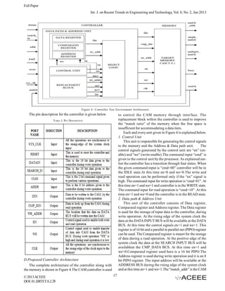
Figure 2: Block diagram
The MATCH_ADDRESS BUS indicates the address that
matches the contents of the CMP_DATA_BUS.Status signals are “busy”, “match”, “single_match” and
“multiple_match”.The “busy” signal will remain asserted
during a write operation and will be low during read operation. The “match” signal will be asserted when the data on
the CMP_DATA_BUS matches data in one or more locations
in the CAM. When more than one match is present in the
CAM “multiple_match” signal is asserted and when there is
only one match “single_match” signal is asserted. During
read operation when the data is not present in any of the
memory locations, then the “match” signal will be low. At
that time the replacement block will carry out the replacement
of the data in a sequential manner starting from the first location.
III. DESIGN METHODOLOGY
A. Introduction
The CAM controller is designed to work with Xilinx®
CAM version 6.1.It has a user interface on one side and the
memory on the other side. The controller architecture consists
of Control unit, Data path & Address unit, a built in
Replacement block to improve the match ratio of the memory
and a Select logic.
C. Pin Description
The Input/output diagram for the controller is shown in
Figure 3.The output ports from the controller are given as
input ports to the memory.
All the pins in the Input/output diagram of the controller
are described in Table I. The direction and the description of
the pins are also given.
B. Block Diagram
The CAM controller is used to control the CAM memory
through interface. The block diagram for the controller along
with the CAM memory is shown in Figure 2.
The controller consists of Control unit, Data path &
Address unit, Replacement block and a Select logic. The
CONTROL SIGNALS from the control unit are given to the
memory and also to the Data path & Address unit. The DATA
INPUT and the SEARCH INPUT to the controller is 16 bit.
The ADDRESS is 8 bit. The CONTROL INPUT is the user
command to the controller and it is of 2 bit. The sys_clk
(system clock) and reset signal is also given to the controller.
The DATA BUS and CMP_DATA_BUS from thecontroller to
the memory is 16 bit. The ADDRESS BUS is 8 bit. The control
signals to the memory and the Data path & Address unit are
“en” (enable) and “we” (write enable) signals.
© 2013 ACEEE
DOI: 01.IJRTET.8.2.28
Figure 3: Input/output diagram for the Controller
16](https://image.slidesharecdn.com/28-140215035900-phpapp01/85/A-Novel-Architecture-Design-Characterization-of-CAM-Controller-IP-Core-with-Replacement-Policy-2-320.jpg)
![Full Paper
Int. J. on Recent Trends in Engineering and Technology, Vol. 8, No. 2, Jan 2013
B. Synthesis Result
Table II shows the power analysis done and Table III
shows the device utilization result.
address where matching data resides. The “match”signal
indicates that at least one location in the CAM contains the
same data as the DATA BUS. The “single_match” signal
indicates the existence of matching data in one location of
the CAM. The “multiple_match” signal indicates the
existence of matching data in more than one locations of the
CAM. The “busy” signal indicates that a write operation is
currently being executed.
3. Replacement Block
This unit is responsible for determining which data item(s)
should be deleted from the memory when the free space is
insufficient for accommodating a data item. It is an important
factor that improves the match ratio of the memory. A
sequential replacement policy is used here.This type of
replacement policy consumes only little power [4]. When the
controller is in the read state the data at the SEARCH INPUT
BUS will be available at the CMP_DATA BUS .The memory
locations will be searched simultaneously for the data. If the
data is not present in any of the memory locations then the
“match” signal will be low. Then the replacement block will
be active. The replacement block simply increments an address
counter sequentially to points to the location of the new
entry [4]. Then the search input data will be written to that
location. To perform this replacement the “en” and the “we”
signal should be high.
4. Select Logic
This unit is responsible for selecting either the outputs
from the replacement block or the outputs from the control
unit and data path & address unit. The outputs from the
replacement block are selected if the data that is searched for
is not present in any of the memory locations. At this time the
“S0” signal will be high. The outputs from the control unit
and data path & address unit will be selected when the data
that is searched for is present in any of the memory locations
and at this time the “S0 signal will be low.
TABLE II. POWER ANALYSIS R EPORT
TABLE III. DEVICE UTILIZATION R EPORT
IV. IMPLEMENTATION AND RESULTS
The hardware test result was obtained using Chip Scope Pro®
logic analyzer and the logic analysis for the write, read and
replacement operation is shown in Figure 6, Figure 7 and
Figure 8.
The design program for the controller with replacement
policy for the CAM v 6.1 of Xilinx® was simulated functionally
verified and synthesized using Xilinx ISE® design suite. The
target device is SPARTAN® 3AN FPGA by Xilinx® [3].
A. Simulation Results
The simulation result for the controller along with the
memory is shown in Figure 5.
Figure 6: Hardware test result for write operation
Figure 5: Simulation result
© 2013 ACEEE
DOI: 01.IJRTET.8.2.28
18](https://image.slidesharecdn.com/28-140215035900-phpapp01/85/A-Novel-Architecture-Design-Characterization-of-CAM-Controller-IP-Core-with-Replacement-Policy-4-320.jpg)
![Full Paper
Int. J. on Recent Trends in Engineering and Technology, Vol. 8, No. 2, Jan 2013
consumption.This work is believed to serve as a good bench
mark for selecting an optimum controller core for the CAM
memory to improve the match ratio.The proposed design has
been tested by implementing the design on SPARTAN 3AN
FPGA board which uses XC3S700AN device.The future work
includes adding a Built-in self testing module to the present
architecture [8].
REFERENCES
[1] Xilinx DS253 Content Addressable Memory v 6.1,Datasheet
available online at http://www.xilinx.com/support/
documentation/cam_ds253.pdf.
[2] A.G Hanlon,”Content Addressable and Assocoative Memory
Systems-A Survey,” IEEE Trans. on Electronic Computers
vol EC-15,no.4,August,1966.
[3]Xilinx,Spartan-3A/3AN FPGA Starter Kit Board User Guide
available online at www.xilinx.com/support/documentation/
boards and kits/ug334.pdf.
[4] Kostas Pagiamtzis, Ali, Ali Sheikholeslami, “Using Cache to
Reduce Power in Content-Addressable Memories (CAMs),”
IEEE CustomIntegrated Circuits Conference, 2005.
[5] Mohammad ShihabulHaque, Jorgen Peddersen, Andhi
Janapsatya, Sri Parameswaran, “DEW: A Fast Level 1 Cache
Simulation Approach for Embedded Processors with FIFO
Replacement Policy,” Design, Automation & Test in Europe
Conference & Exhibition, 2010.
[6] JianliangXu, QinglongHu, Wang-Chien Lee, DikLun Lee,
“Performance Evaluation of an Optimal Cache Replacement
Policy for Wireless Data Dissemination,”IEEE Trans. on
Knowledge and Data Engineering.vol.16, Jan.2004.
[7] MohdWajid, Shahank SB, “Architecture for Faster RAM
Controller Design with Inbuilt Memory,” Second International
Conference on Computational Intelligence, Communication
Systems and Networks, 2010.
[8] Kun-Jin Lin,Cheng-Wen Wu, “Testing Content-Addressable
Memories Using Functional Fault Models and March-Like
Test Algorithms,” IEEE Trans.on Computer Aided Design of
Integrated Circuits and Systems, vol.19 no.5,May,2000.
Figure 7: Hardware test result for read operation
Figure 8: Hardware test result for replacement operation
V. CONCLUSION
Content Addressable Memory (CAM) is a special purpose
Random Access Memory (RAM) device that can be accessed
by searching for data content. The architecture of a custom
controller with replacement policy for the Content
Addressable Memory was designed,prototyped and
characterized for resourse utilization and power
© 2013 ACEEE
DOI: 01.IJRTET.8.2. 28
19](https://image.slidesharecdn.com/28-140215035900-phpapp01/85/A-Novel-Architecture-Design-Characterization-of-CAM-Controller-IP-Core-with-Replacement-Policy-5-320.jpg)