Downloaded 1,806 times

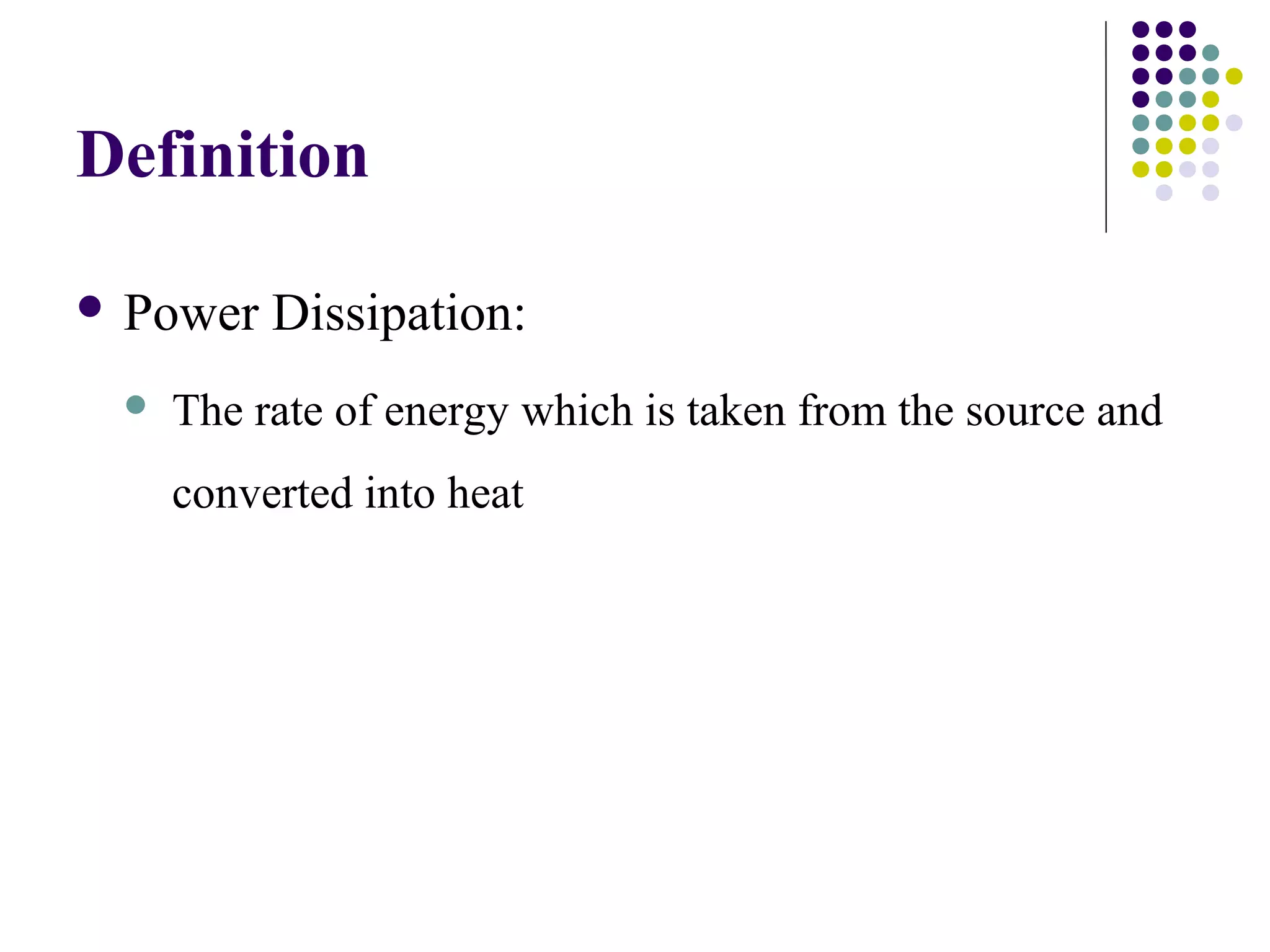
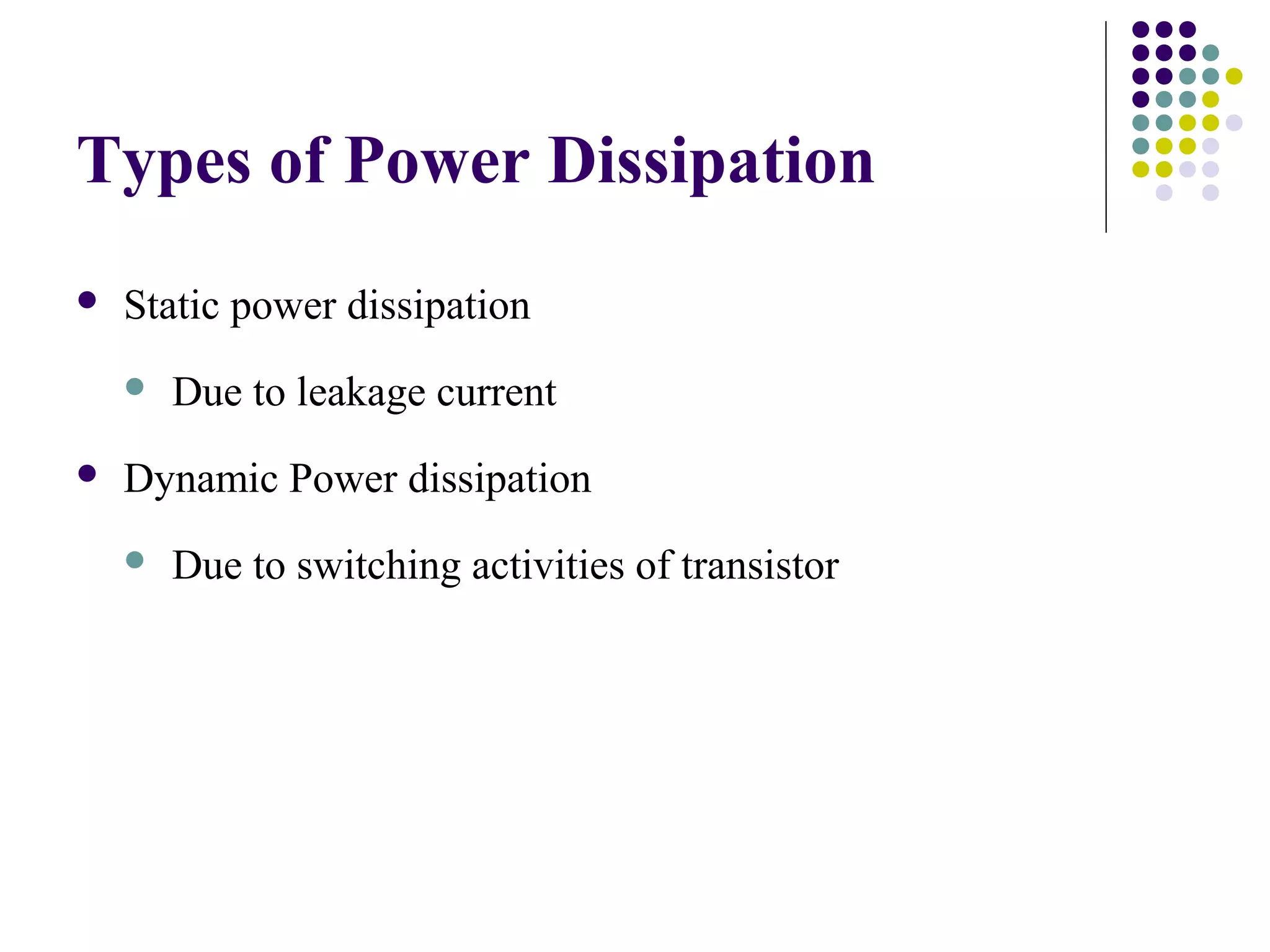
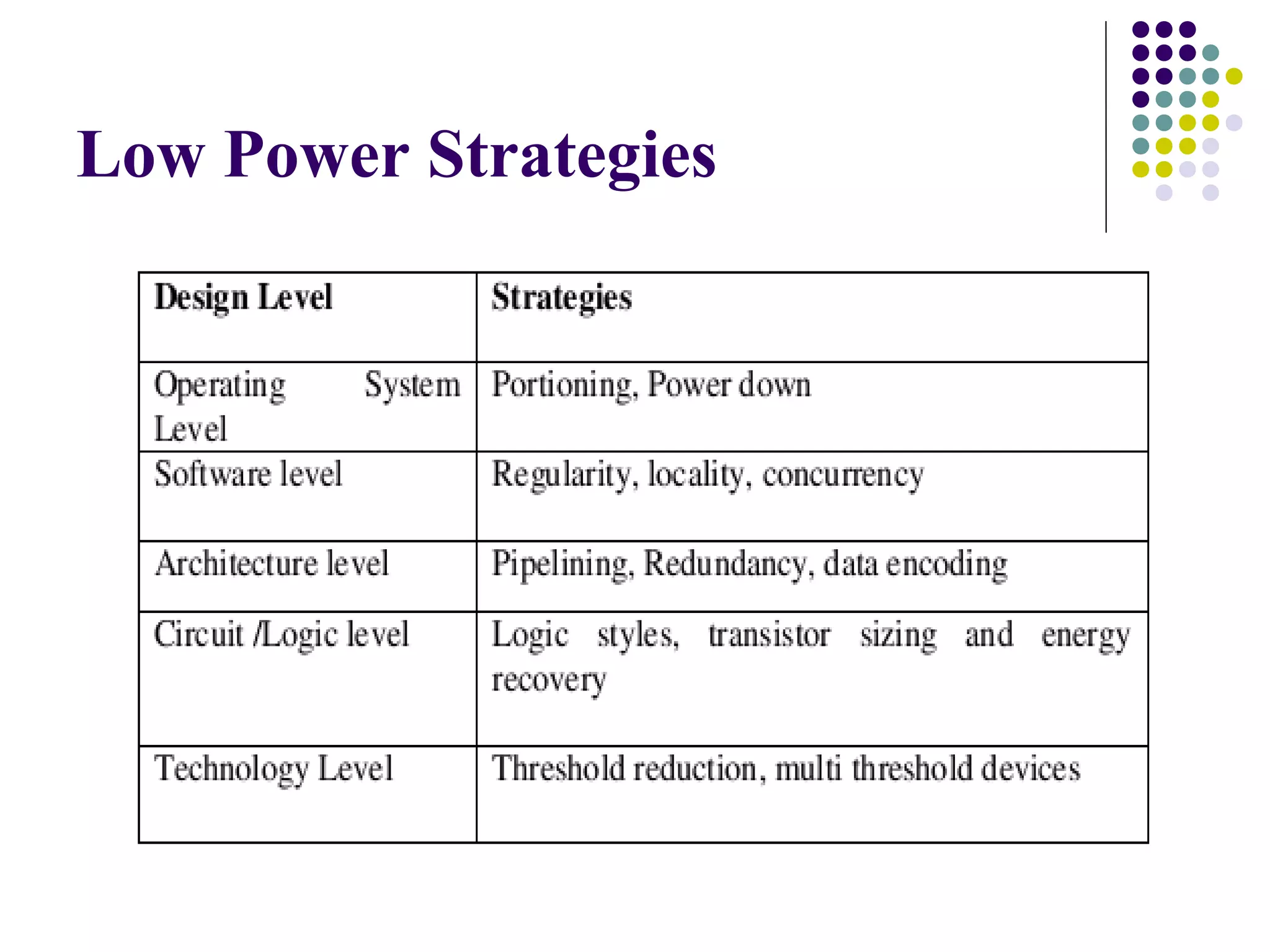
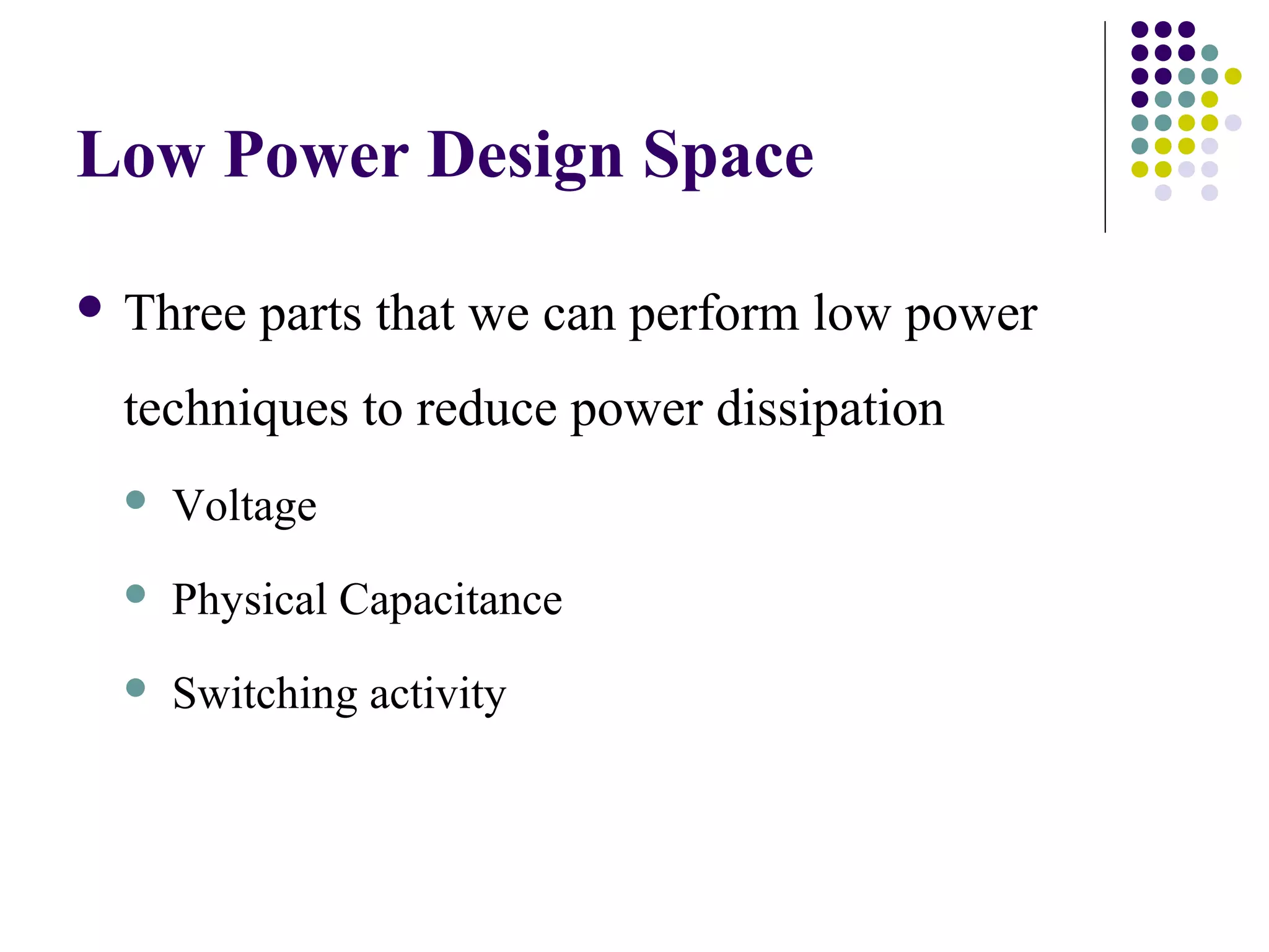
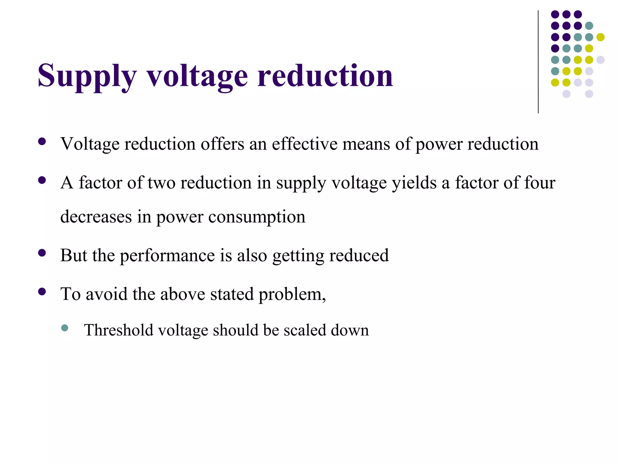
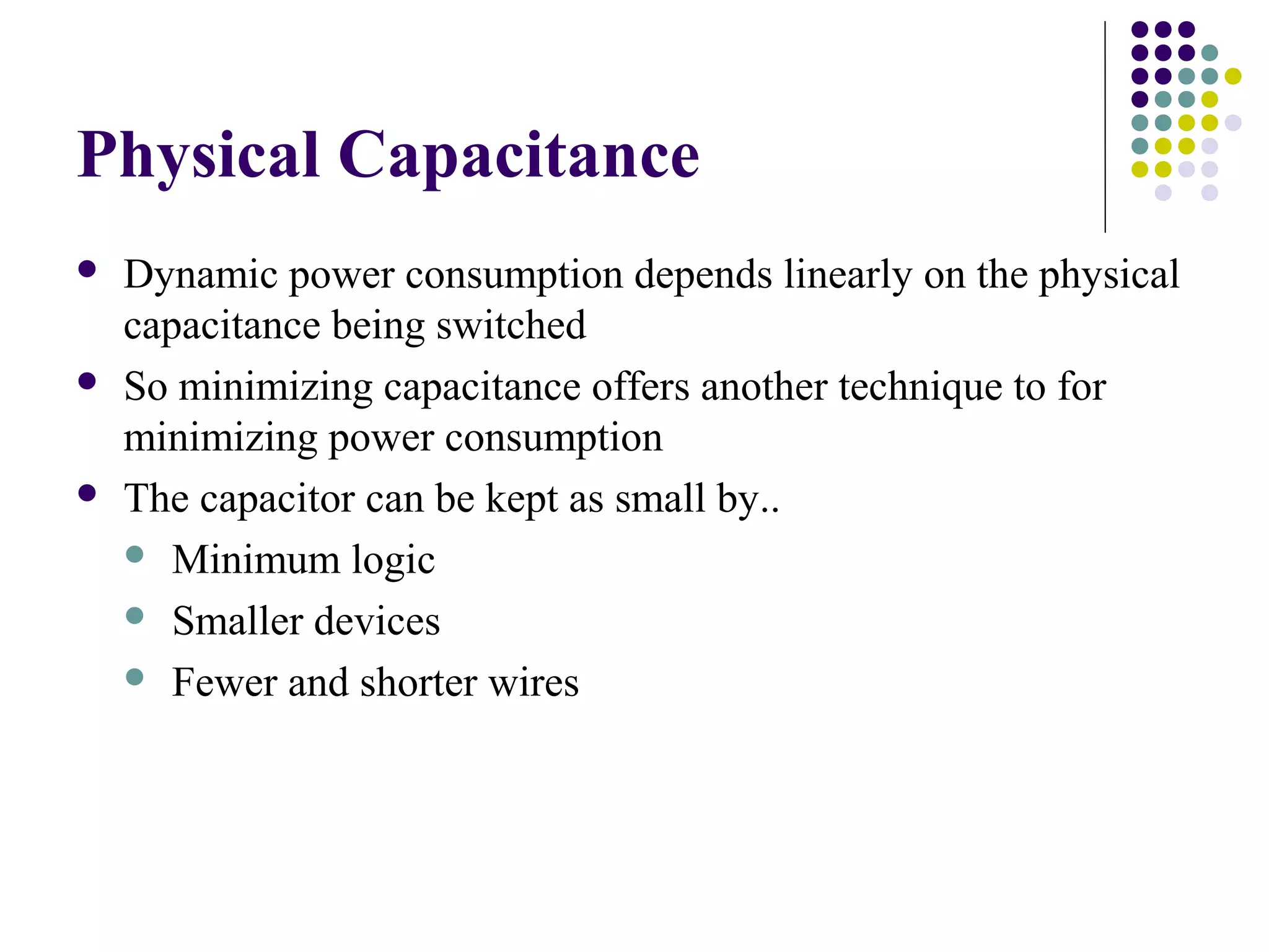
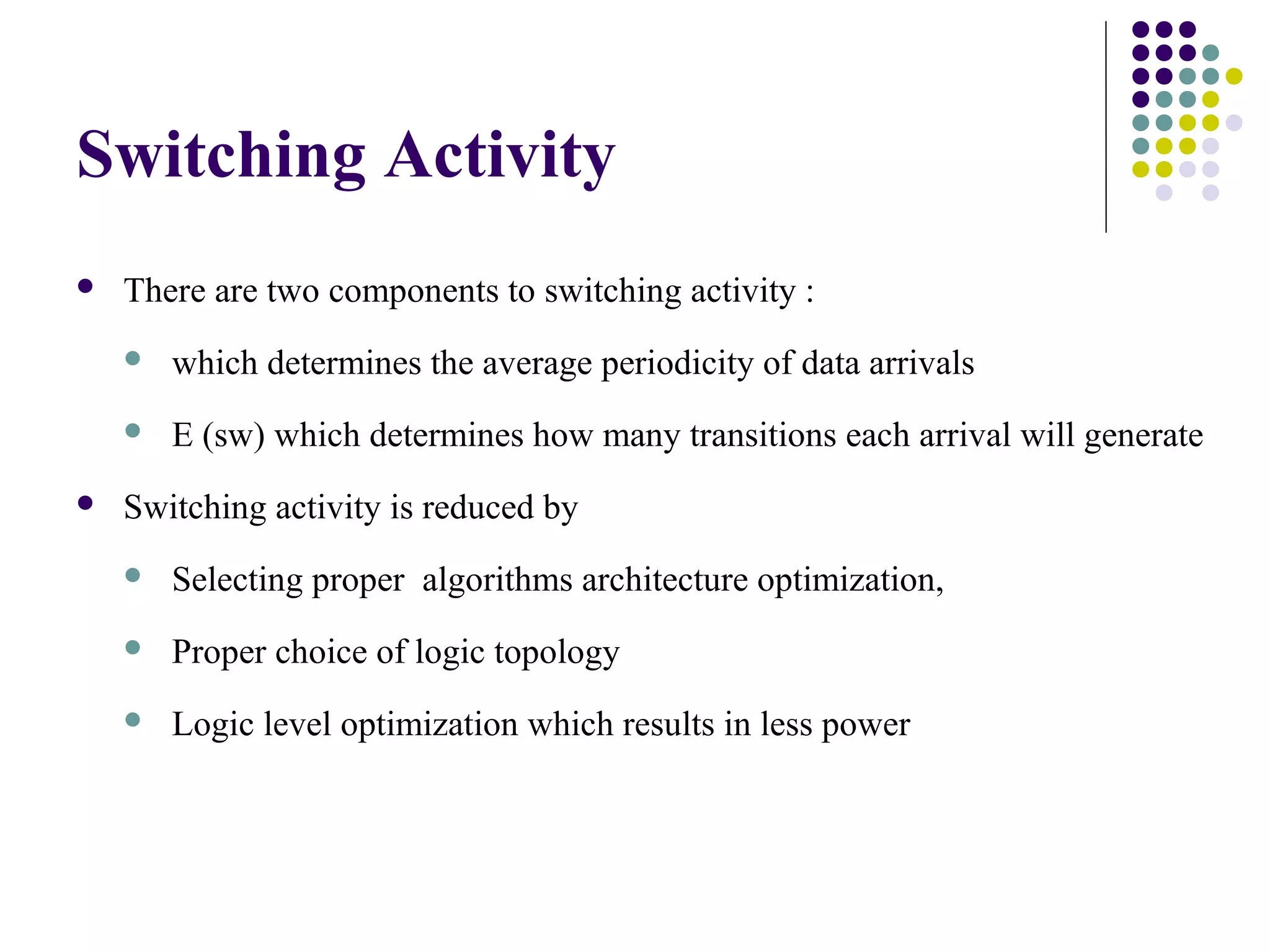
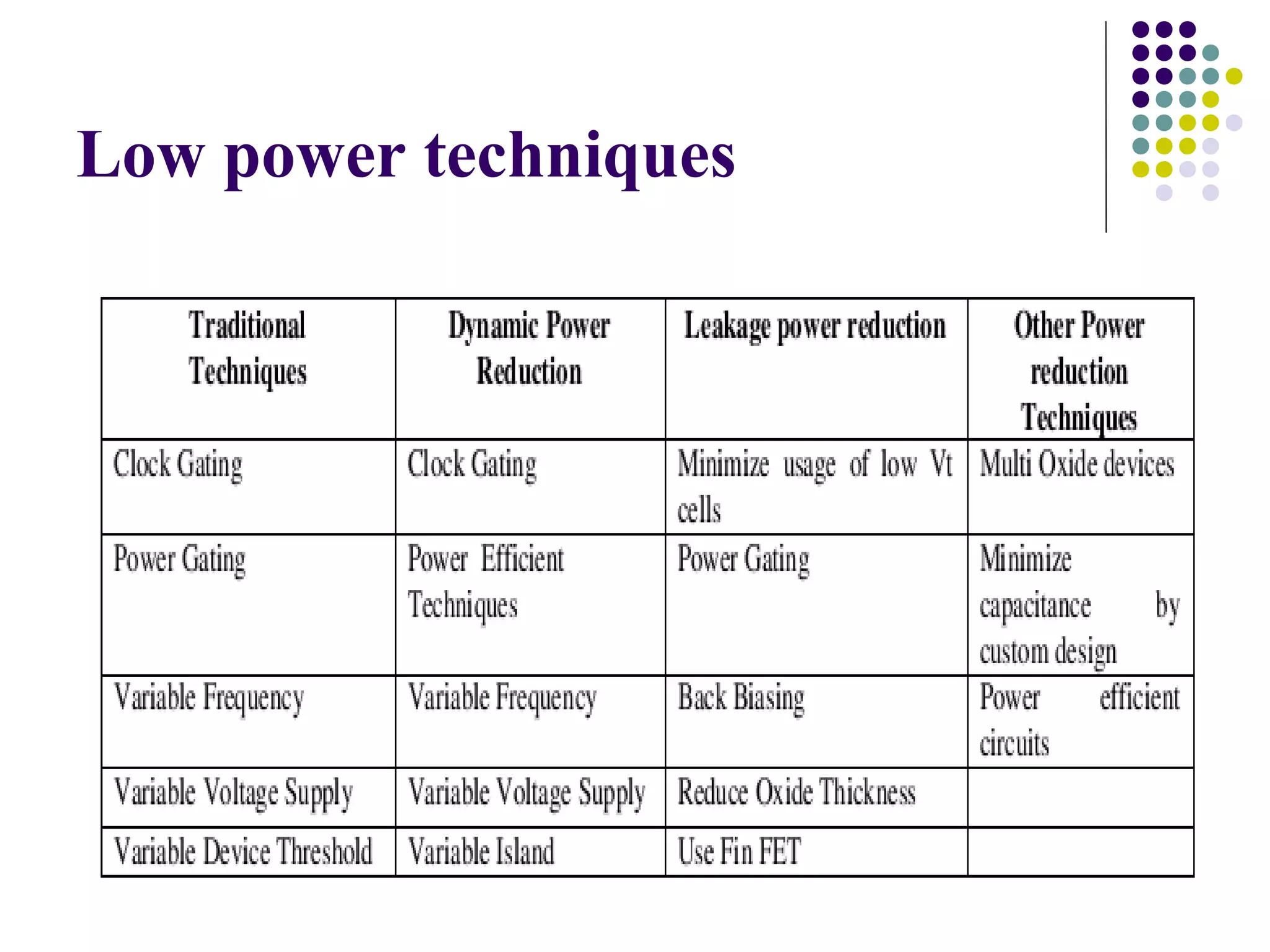
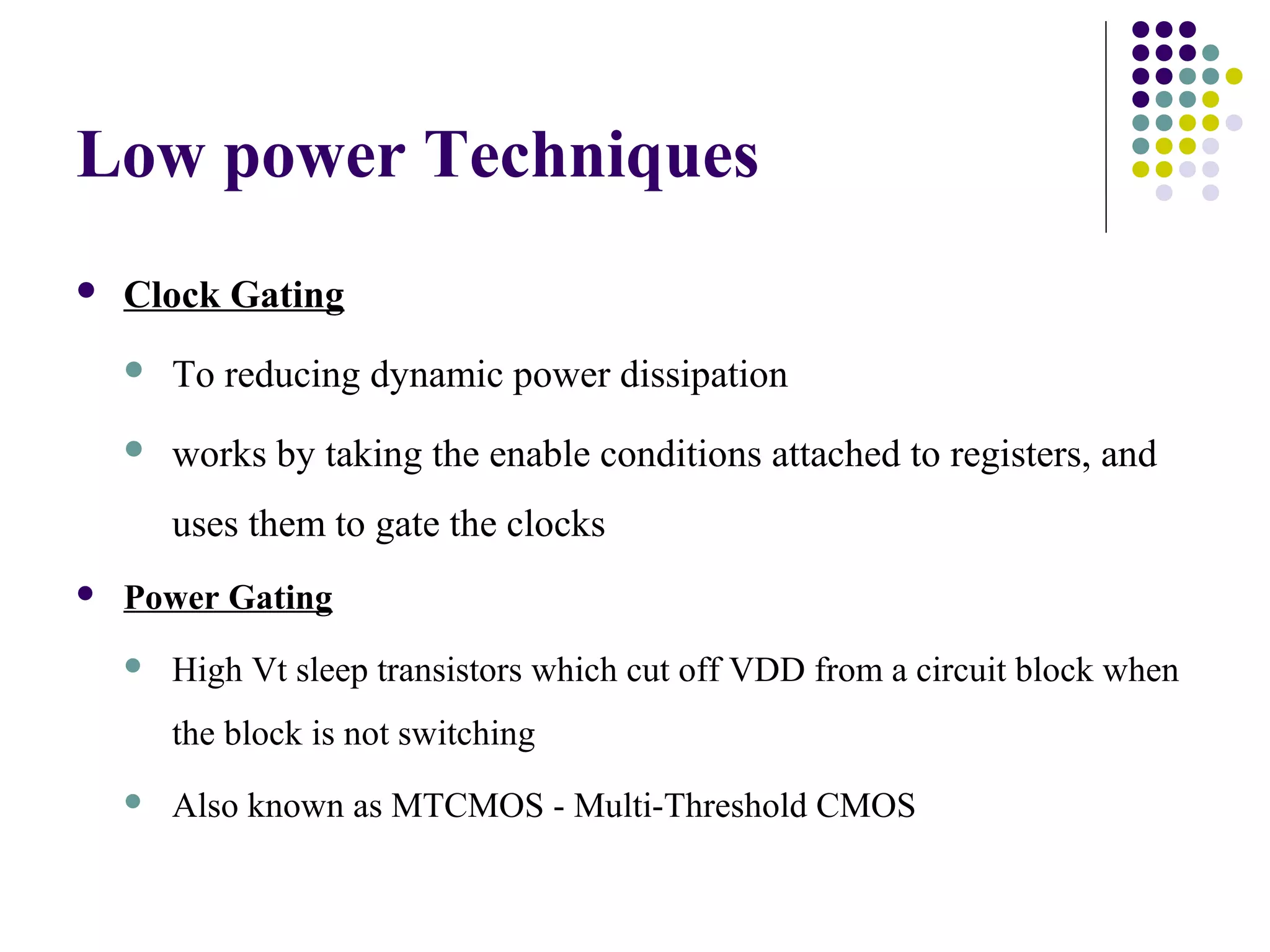
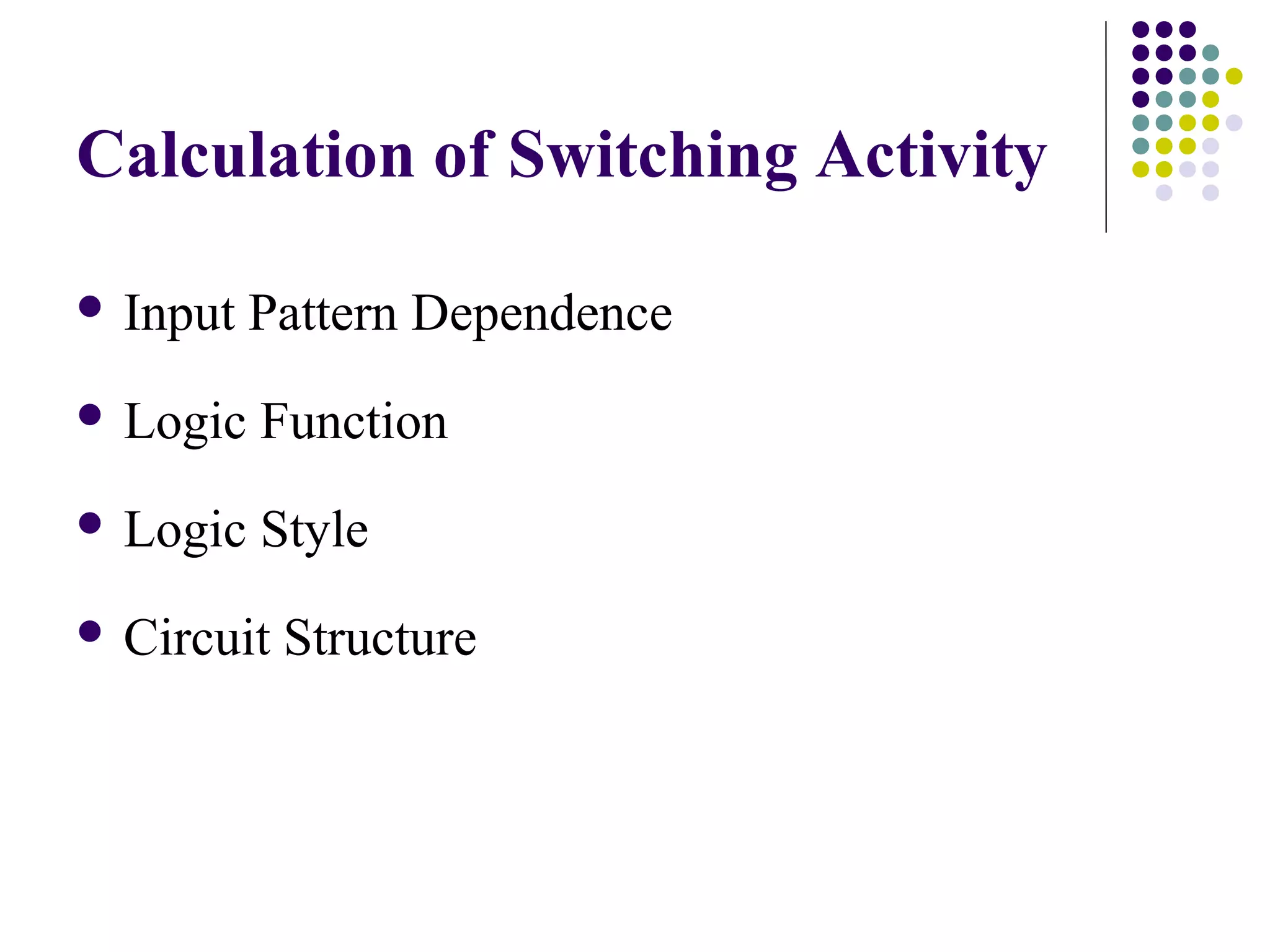
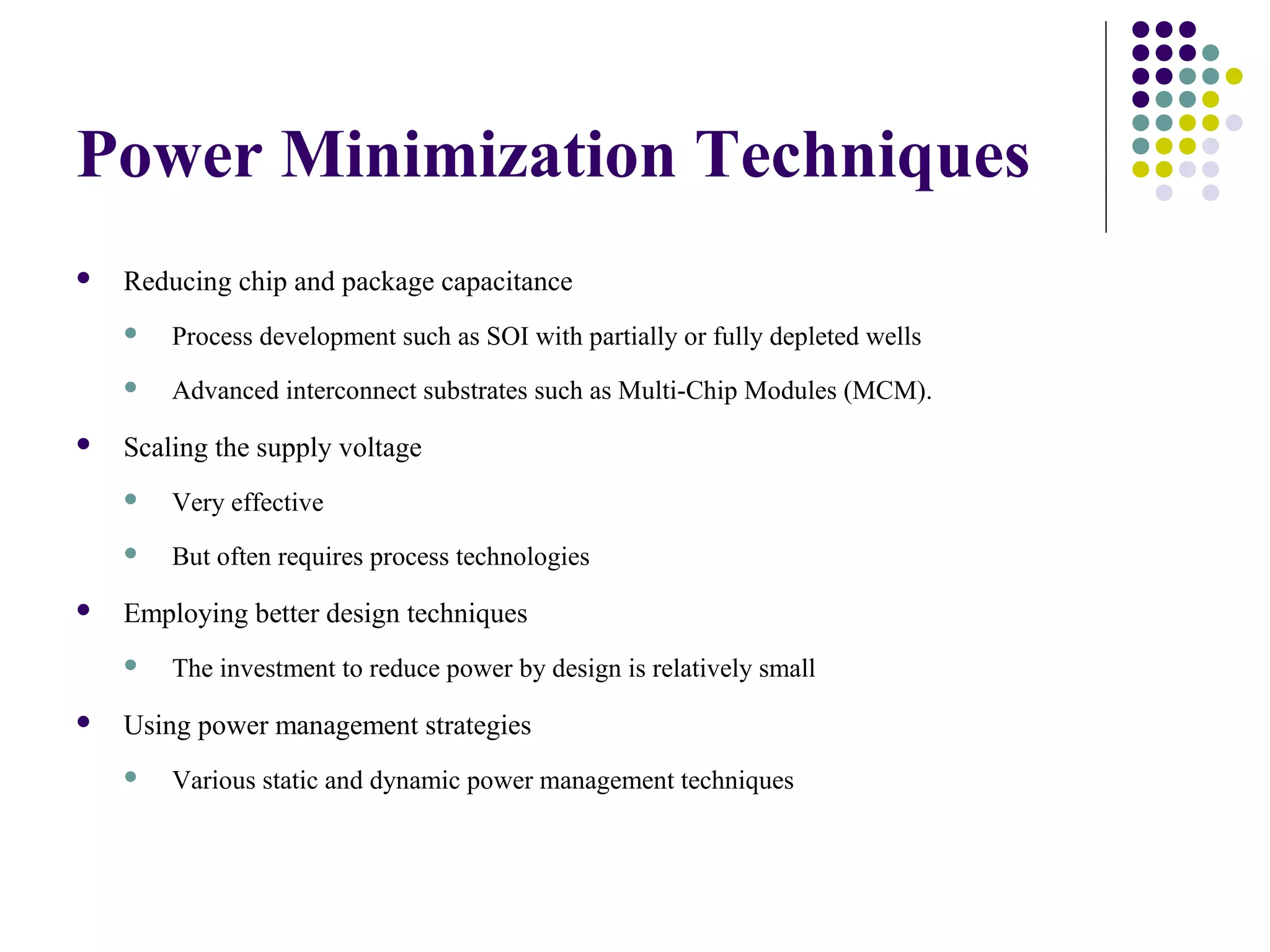
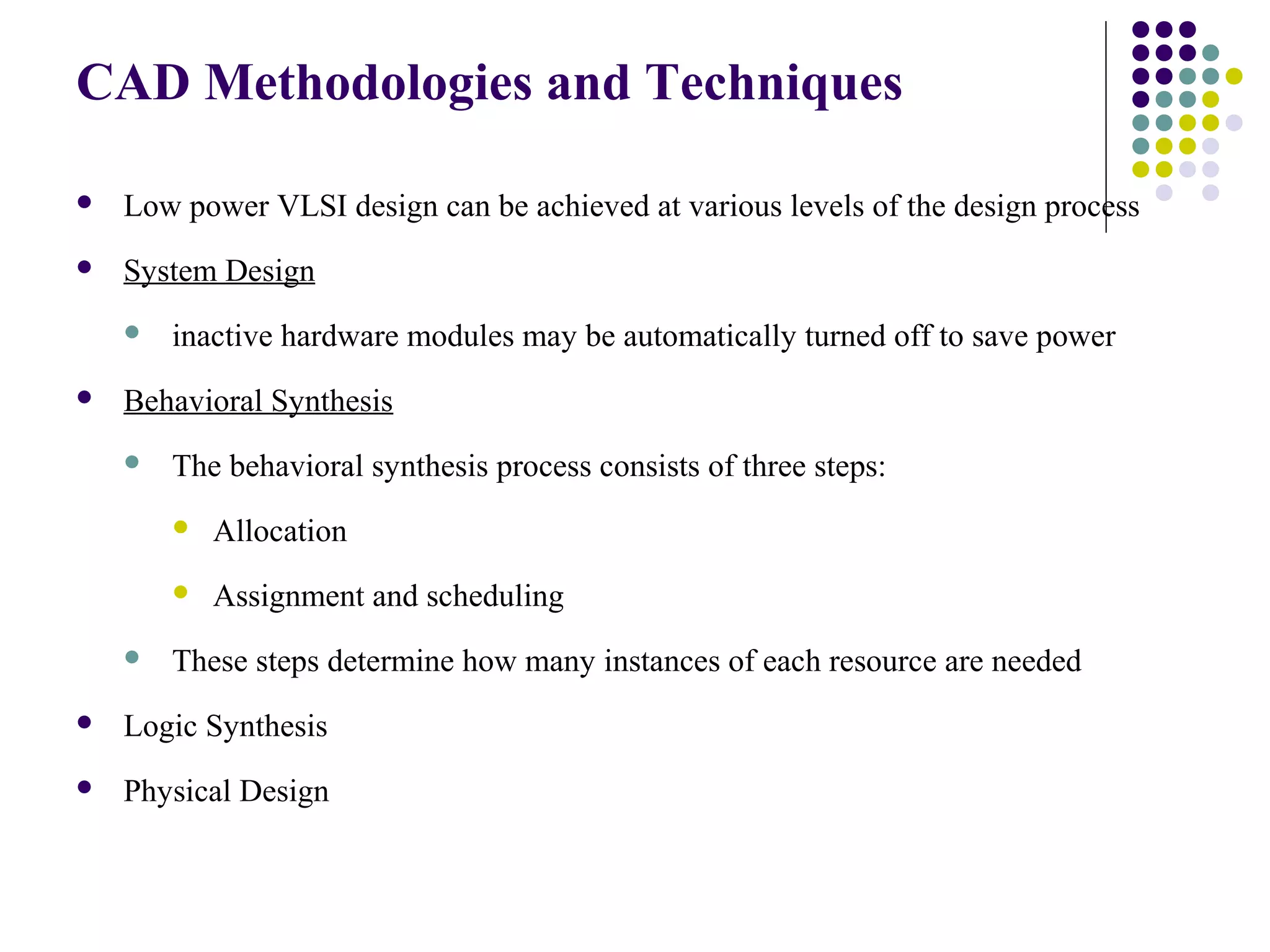
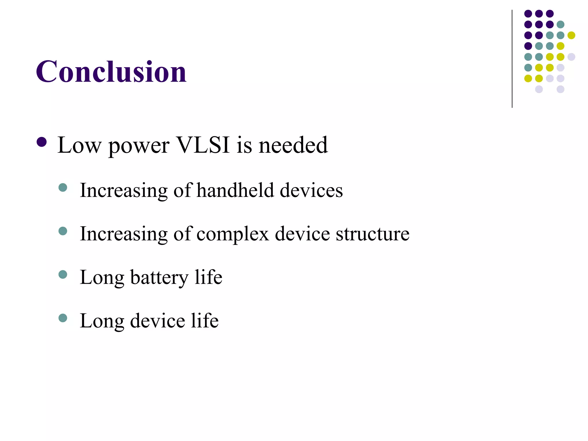


This document discusses low power VLSI design. It defines power dissipation as being either static, from leakage current, or dynamic, from transistor switching activities. The key strategies for low power design are reducing supply voltage, physical capacitance, and switching activity. Specific techniques mentioned include clock gating, power gating, reducing chip capacitance, scaling voltage, better design methods, and power management. The document also discusses calculating and minimizing switching activity and using CAD tools at different design levels.