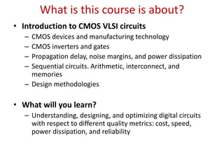
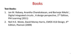
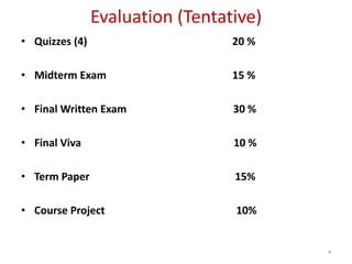
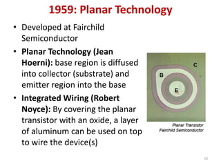
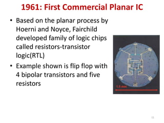
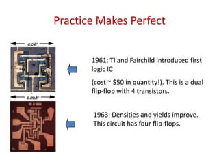
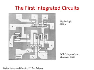
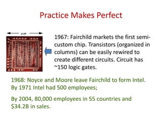
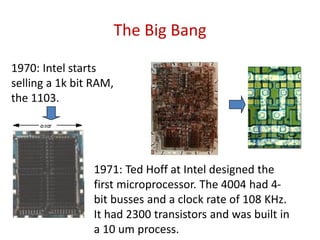
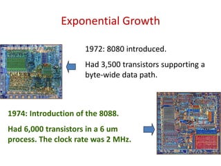
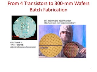
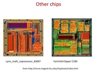
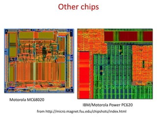
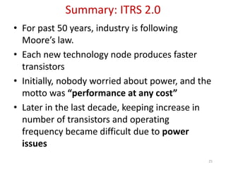
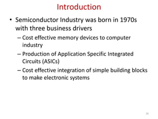
VLSI Design
(Course Code: EEL3320)
Lectures 1-3:
Introduction : Evolution of Design
Course Instructor:
Shree Prakash Tiwari, Ph.D.
Email: sptiwari@iitj.ac.in
Webpage: http://home.iitj.ac.in/~sptiwari/
Indian Institute of Technology Jodhpur, Year 2023
1
Note: The information provided in the slides are taken mainly form two text books of VLSI
Design(Jan M. Rabaey, .. & Neil H. Weste, …), ITRS 2.0, and other resources from internet, for
teaching/academic use only
What is this course is about?
• Introduction to CMOS VLSI circuits
– CMOS devices and manufacturing technology
– CMOS inverters and gates
– Propagation delay, noise margins, and power dissipation
– Sequential circuits. Arithmetic, interconnect, and
memories
– Design methodologies
• What will you learn?
– Understanding, designing, and optimizing digital circuits
with respect to different quality metrics: cost, speed,
power dissipation, and reliability
Books
Text Books:
1. Jan M. Rabaey, Anantha Chandrakasan, and Borivoje Nikolic´,
Digital integrated circuits , A design perspective, 2nd Edition,
PHI Learning (2011)
2. Neil H.E. Weste, David Money Harris, CMOS VLSI Design, 4th
Edition, Pearson (2009)
3
Evaluation (Tentative)
• Quizzes (4) 20 %
• Midterm Exam 15 %
• Final Written Exam 30 %
• Final Viva 10 %
• Term Paper 15%
• Course Project 10%
4
Brief History
The First Computer: Babbage Difference Engine (1832)
•Executed basic operations
(add, sub, mult, div) in arbitrary
sequences
•Operated in two-cycle
sequence, “Store”, and “Mill”
(execute)
•Included features like
pipelining to make it faster.
•Complexity: 25,000 parts.
The Electrical Solution
•More cost effective
•Early systems used relays to make simple logic devices
•Still used today in some train safety systems
•The Vacuum Tube
•Originally used for analog processing
•Later, complete digital computers realized
High Point of Tubes: The ENIAC (Electronic Numerical Integrator And
Computer)
•18,000 vacuum tubes
•80 ft long, 8.5 ft high, several feet wide
ENIAC - The first electronic computer (1946)
Dawn of the Transistor Age
1951: Shockley develops junction
transistor which can be
manufactured in quantity.
1947: Bardeen and Brattain
create point-contact transistor
w/two PN junctions. Gain = 18
Evolution of IC
9
Bardeen, Brattain, and
Shockley (Seated) @ Bell
Laboratories, 1948. The Nobel
prize was given in 1956.
First Point contact
Transistor (1947, Bell
Labs) with Germanium
semiconductor, and
two gold contacts
separated by 50
micron.
First IC, Developed
independently by
J. Kilby (Texas Instruments) and
R. Noyce, J. Hoerni (Fairchild
Semiconductor), 1958.
Co-recipient of
Nobel prize
in physics in 2000
1959: Planar Technology
• Developed at Fairchild
Semiconductor
• Planar Technology (Jean
Hoerni): base region is diffused
into collector (substrate) and
emitter region into the base
• Integrated Wiring (Robert
Noyce): By covering the planar
transistor with an oxide, a layer
of aluminum can be used on top
to wire the device(s)
10
1961: First Commercial Planar IC
• Based on the planar process by
Hoerni and Noyce, Fairchild
developed family of logic chips
called resistors-transistor
logic(RTL)
• Example shown is flip flop with
4 bipolar transistors and five
resistors
11
Practice Makes Perfect
1961: TI and Fairchild introduced first
logic IC
(cost ~ $50 in quantity!). This is a dual
flip-flop with 4 transistors.
1963: Densities and yields improve.
This circuit has four flip-flops.
13
The First Integrated Circuits
Bipolar logic
1960’s
ECL 3-input Gate
Motorola 1966
Digital Integrated Circuits, 2nd Ed., Rabaey.
Practice Makes Perfect
1967: Fairchild markets the first semi-
custom chip. Transistors (organized in
columns) can be easily rewired to
create different circuits. Circuit has
~150 logic gates.
1968: Noyce and Moore leave Fairchild to form Intel.
By 1971 Intel had 500 employees;
By 2004, 80,000 employees in 55 countries and
$34.2B in sales.
The Big Bang
1970: Intel starts
selling a 1k bit RAM,
the 1103.
1971: Ted Hoff at Intel designed the
first microprocessor. The 4004 had 4-
bit busses and a clock rate of 108 KHz.
It had 2300 transistors and was built in
a 10 um process.
Exponential Growth
1972: 8080 introduced.
Had 3,500 transistors supporting a
byte-wide data path.
1974: Introduction of the 8088.
Had 6,000 transistors in a 6 um
process. The clock rate was 2 MHz.
From 4 Transistors to 300-mm Wafers
Batch Fabrication
17
What is a VLSI IC?
VERY LARGE SCALE Integration
A circuit that has 10k ~ 1Bln
transistors on a single chip
•Still growing as number of
transistors on chip
quadruple every 24 months
(Moore’s law!)
Technique where many
circuit components and the
wiring that connects them
are manufactured
simultaneously on a
compact chip (die)
INTEGRATED CIRCUIT
Today
Many disciplines have contributed to the current state of the art in
VLSI Design:
•Solid State Physics
•Materials Science
•Lithography and fab
•Device modeling
•Circuit design and
layout
•Architecture design
•Algorithms
•CAD tools
To come up with chips like:
Pentium 4
– Introduction date: November
20, 2000
• 1.4 GHz clock
• fabricated in 180 nm process,
• 42 mln transistors)
– In 2002 (2 GHz in 130 nm, 55
mln transistors)
– In 2005 (3.8 GHz in 90 nm, 125
mln transistors)
– Typical Use: Desktops and
entry-level workstations
•In 2006
•143 mm2
•3 GHZ operation
•65 nm CMOS
technology
•291 mln transistors
Intel Core 2 Microprocessor
Other chips
from http://micro.magnet.fsu.edu/chipshots/index.html
cyrix_math_coprocessor_83S87 Fairchild Clipper C100
Other chips
from http://micro.magnet.fsu.edu/chipshots/index.html
Motorola MC68020
IBM/Motorola Power PC620
International Technology Roadmap for
Semiconductors(ITRS)
• ITRS is a set of reports and documents produced by a group
of semiconductor industry experts.
• These experts are representative of the sponsoring
organisations which include the Semiconductor Industry
Associations of the United States, Europe, Japan, South
Korea and Taiwan.
24
Ref. ITRS 2.0, 2015
Summary: ITRS 2.0
• For past 50 years, industry is following
Moore’s law.
• Each new technology node produces faster
transistors
• Initially, nobody worried about power, and the
motto was “performance at any cost”
• Later in the last decade, keeping increase in
number of transistors and operating
frequency became difficult due to power
issues
25
Introduction
• Semiconductor Industry was born in 1970s
with three business drivers
– Cost effective memory devices to computer
industry
– Production of Application Specific Integrated
Circuits (ASICs)
– Cost effective integration of simple building blocks
to make electronic systems
26
Moore’s Law
• In 1965, Gordon Moore noted that the
number of transistors on a chip doubled every
18 to 24 months.
• He made a prediction that semiconductor
technology will double its effectiveness every
18 months
27
The Ever Shrinking Transistor
28
Using 45 nm technology, ≈ 400 transistors fit on a red blood cell!
Moore’s law in Microprocessors
4004
8008
8080
8085 8086
286
386
486
Pentium® proc
P6
0.001
0.01
0.1
1
10
100
1000
1970 1980 1990 2000 2010
Year
Transistors
(MT)
2X growth in 1.96 years!
Transistors on Lead Microprocessors double every 2 years
Courtesy, Intel
Die Size Growth
4004
8008
8080
8085
8086
286
386
486 Pentium ® proc
P6
1
10
100
1970 1980 1990 2000 2010
Year
Die
size
(mm)
~7% growth per year
~2X growth in 10 years
Die size grows by 14% to satisfy Moore’s Law
Courtesy, Intel
Power dissipation warning in 2000
5KW
18KW
1.5KW
500W
4004
8008
8080
8085
8086
286
386
486
Pentium® proc
0.1
1
10
100
1000
10000
100000
1971 1974 1978 1985 1992 2000 2004 2008
Year
Power
(Watts)
Did this really happen?
Courtesy, Intel
Power density
4004
8008
8080
8085
8086
286
386
486
Pentium® proc
P6
1
10
100
1000
10000
1970 1980 1990 2000 2010
Year
Power
Density
(W/cm2)
Hot Plate
Nuclear
Reactor
Rocket
Nozzle
Power density too high to keep junctions at low temp
Courtesy, Intel
New devices
such as Tunnel
FETs !!!
No Moore’s Law in future!!
33
Digital Cellular Market
(Phones Shipped)
1996 1997 1998 1999 2000
Units 48M 86M 162M 260M 435M
Cell
Phones
Not Only Microprocessors
iPod
Video games
Analog
Baseband
Digital Baseband
(DSP + MCU)
Power
Management
Small
Signal RF
Power
RF
iTablet
Today’s Electronic Products:
Result of Heterogeneous Integration
35
Example: IoT Driver
36
Challenges in Digital Design
“Microscopic Problems”
• Ultra-high speed design
• Interconnect
• Noise, Crosstalk
• Reliability, Manufacturability
• Power Dissipation
• Clock distribution.
Everything Looks a Little Different
“Macroscopic Issues”
• Time-to-Market
• Millions of Gates
• High-Level Abstractions
• Reuse & IP: Portability
• Predictability
• etc.
…and There’s a Lot of Them!
Design Abstraction Levels
n+
n+
S
G
D
+
DEVICE
CIRCUIT
GATE
MODULE
SYSTEM
What next
Summary
• VLSI Design will be continuing for next many
years
• Proper understanding and Training for CMOS
and VLSI is required
• Research for new device designs and materials
is necessary
• Exploratory work should also be encouraged
for new technologies
40

L1,2,3.pdf

  • 1.
    VLSI Design (Course Code:EEL3320) Lectures 1-3: Introduction : Evolution of Design Course Instructor: Shree Prakash Tiwari, Ph.D. Email: sptiwari@iitj.ac.in Webpage: http://home.iitj.ac.in/~sptiwari/ Indian Institute of Technology Jodhpur, Year 2023 1 Note: The information provided in the slides are taken mainly form two text books of VLSI Design(Jan M. Rabaey, .. & Neil H. Weste, …), ITRS 2.0, and other resources from internet, for teaching/academic use only
  • 2.
    What is thiscourse is about? • Introduction to CMOS VLSI circuits – CMOS devices and manufacturing technology – CMOS inverters and gates – Propagation delay, noise margins, and power dissipation – Sequential circuits. Arithmetic, interconnect, and memories – Design methodologies • What will you learn? – Understanding, designing, and optimizing digital circuits with respect to different quality metrics: cost, speed, power dissipation, and reliability
  • 3.
    Books Text Books: 1. JanM. Rabaey, Anantha Chandrakasan, and Borivoje Nikolic´, Digital integrated circuits , A design perspective, 2nd Edition, PHI Learning (2011) 2. Neil H.E. Weste, David Money Harris, CMOS VLSI Design, 4th Edition, Pearson (2009) 3
  • 4.
    Evaluation (Tentative) • Quizzes(4) 20 % • Midterm Exam 15 % • Final Written Exam 30 % • Final Viva 10 % • Term Paper 15% • Course Project 10% 4
  • 5.
    Brief History The FirstComputer: Babbage Difference Engine (1832) •Executed basic operations (add, sub, mult, div) in arbitrary sequences •Operated in two-cycle sequence, “Store”, and “Mill” (execute) •Included features like pipelining to make it faster. •Complexity: 25,000 parts.
  • 6.
    The Electrical Solution •Morecost effective •Early systems used relays to make simple logic devices •Still used today in some train safety systems •The Vacuum Tube •Originally used for analog processing •Later, complete digital computers realized High Point of Tubes: The ENIAC (Electronic Numerical Integrator And Computer) •18,000 vacuum tubes •80 ft long, 8.5 ft high, several feet wide
  • 7.
    ENIAC - Thefirst electronic computer (1946)
  • 8.
    Dawn of theTransistor Age 1951: Shockley develops junction transistor which can be manufactured in quantity. 1947: Bardeen and Brattain create point-contact transistor w/two PN junctions. Gain = 18
  • 9.
    Evolution of IC 9 Bardeen,Brattain, and Shockley (Seated) @ Bell Laboratories, 1948. The Nobel prize was given in 1956. First Point contact Transistor (1947, Bell Labs) with Germanium semiconductor, and two gold contacts separated by 50 micron. First IC, Developed independently by J. Kilby (Texas Instruments) and R. Noyce, J. Hoerni (Fairchild Semiconductor), 1958. Co-recipient of Nobel prize in physics in 2000
  • 10.
    1959: Planar Technology •Developed at Fairchild Semiconductor • Planar Technology (Jean Hoerni): base region is diffused into collector (substrate) and emitter region into the base • Integrated Wiring (Robert Noyce): By covering the planar transistor with an oxide, a layer of aluminum can be used on top to wire the device(s) 10
  • 11.
    1961: First CommercialPlanar IC • Based on the planar process by Hoerni and Noyce, Fairchild developed family of logic chips called resistors-transistor logic(RTL) • Example shown is flip flop with 4 bipolar transistors and five resistors 11
  • 12.
    Practice Makes Perfect 1961:TI and Fairchild introduced first logic IC (cost ~ $50 in quantity!). This is a dual flip-flop with 4 transistors. 1963: Densities and yields improve. This circuit has four flip-flops.
  • 13.
    13 The First IntegratedCircuits Bipolar logic 1960’s ECL 3-input Gate Motorola 1966 Digital Integrated Circuits, 2nd Ed., Rabaey.
  • 14.
    Practice Makes Perfect 1967:Fairchild markets the first semi- custom chip. Transistors (organized in columns) can be easily rewired to create different circuits. Circuit has ~150 logic gates. 1968: Noyce and Moore leave Fairchild to form Intel. By 1971 Intel had 500 employees; By 2004, 80,000 employees in 55 countries and $34.2B in sales.
  • 15.
    The Big Bang 1970:Intel starts selling a 1k bit RAM, the 1103. 1971: Ted Hoff at Intel designed the first microprocessor. The 4004 had 4- bit busses and a clock rate of 108 KHz. It had 2300 transistors and was built in a 10 um process.
  • 16.
    Exponential Growth 1972: 8080introduced. Had 3,500 transistors supporting a byte-wide data path. 1974: Introduction of the 8088. Had 6,000 transistors in a 6 um process. The clock rate was 2 MHz.
  • 17.
    From 4 Transistorsto 300-mm Wafers Batch Fabrication 17
  • 18.
    What is aVLSI IC? VERY LARGE SCALE Integration A circuit that has 10k ~ 1Bln transistors on a single chip •Still growing as number of transistors on chip quadruple every 24 months (Moore’s law!) Technique where many circuit components and the wiring that connects them are manufactured simultaneously on a compact chip (die) INTEGRATED CIRCUIT
  • 19.
    Today Many disciplines havecontributed to the current state of the art in VLSI Design: •Solid State Physics •Materials Science •Lithography and fab •Device modeling •Circuit design and layout •Architecture design •Algorithms •CAD tools To come up with chips like:
  • 20.
    Pentium 4 – Introductiondate: November 20, 2000 • 1.4 GHz clock • fabricated in 180 nm process, • 42 mln transistors) – In 2002 (2 GHz in 130 nm, 55 mln transistors) – In 2005 (3.8 GHz in 90 nm, 125 mln transistors) – Typical Use: Desktops and entry-level workstations
  • 21.
    •In 2006 •143 mm2 •3GHZ operation •65 nm CMOS technology •291 mln transistors Intel Core 2 Microprocessor
  • 22.
  • 23.
  • 24.
    International Technology Roadmapfor Semiconductors(ITRS) • ITRS is a set of reports and documents produced by a group of semiconductor industry experts. • These experts are representative of the sponsoring organisations which include the Semiconductor Industry Associations of the United States, Europe, Japan, South Korea and Taiwan. 24 Ref. ITRS 2.0, 2015
  • 25.
    Summary: ITRS 2.0 •For past 50 years, industry is following Moore’s law. • Each new technology node produces faster transistors • Initially, nobody worried about power, and the motto was “performance at any cost” • Later in the last decade, keeping increase in number of transistors and operating frequency became difficult due to power issues 25
  • 26.
    Introduction • Semiconductor Industrywas born in 1970s with three business drivers – Cost effective memory devices to computer industry – Production of Application Specific Integrated Circuits (ASICs) – Cost effective integration of simple building blocks to make electronic systems 26
  • 27.
    Moore’s Law • In1965, Gordon Moore noted that the number of transistors on a chip doubled every 18 to 24 months. • He made a prediction that semiconductor technology will double its effectiveness every 18 months 27
  • 28.
    The Ever ShrinkingTransistor 28 Using 45 nm technology, ≈ 400 transistors fit on a red blood cell!
  • 29.
    Moore’s law inMicroprocessors 4004 8008 8080 8085 8086 286 386 486 Pentium® proc P6 0.001 0.01 0.1 1 10 100 1000 1970 1980 1990 2000 2010 Year Transistors (MT) 2X growth in 1.96 years! Transistors on Lead Microprocessors double every 2 years Courtesy, Intel
  • 30.
    Die Size Growth 4004 8008 8080 8085 8086 286 386 486Pentium ® proc P6 1 10 100 1970 1980 1990 2000 2010 Year Die size (mm) ~7% growth per year ~2X growth in 10 years Die size grows by 14% to satisfy Moore’s Law Courtesy, Intel
  • 31.
    Power dissipation warningin 2000 5KW 18KW 1.5KW 500W 4004 8008 8080 8085 8086 286 386 486 Pentium® proc 0.1 1 10 100 1000 10000 100000 1971 1974 1978 1985 1992 2000 2004 2008 Year Power (Watts) Did this really happen? Courtesy, Intel
  • 32.
    Power density 4004 8008 8080 8085 8086 286 386 486 Pentium® proc P6 1 10 100 1000 10000 19701980 1990 2000 2010 Year Power Density (W/cm2) Hot Plate Nuclear Reactor Rocket Nozzle Power density too high to keep junctions at low temp Courtesy, Intel New devices such as Tunnel FETs !!!
  • 33.
    No Moore’s Lawin future!! 33
  • 34.
    Digital Cellular Market (PhonesShipped) 1996 1997 1998 1999 2000 Units 48M 86M 162M 260M 435M Cell Phones Not Only Microprocessors iPod Video games Analog Baseband Digital Baseband (DSP + MCU) Power Management Small Signal RF Power RF iTablet
  • 35.
    Today’s Electronic Products: Resultof Heterogeneous Integration 35
  • 36.
  • 37.
    Challenges in DigitalDesign “Microscopic Problems” • Ultra-high speed design • Interconnect • Noise, Crosstalk • Reliability, Manufacturability • Power Dissipation • Clock distribution. Everything Looks a Little Different “Macroscopic Issues” • Time-to-Market • Millions of Gates • High-Level Abstractions • Reuse & IP: Portability • Predictability • etc. …and There’s a Lot of Them!
  • 38.
  • 39.
  • 40.
    Summary • VLSI Designwill be continuing for next many years • Proper understanding and Training for CMOS and VLSI is required • Research for new device designs and materials is necessary • Exploratory work should also be encouraged for new technologies 40