
Recommended
More Related Content
What's hot
What's hot (20)
Viewers also liked
Viewers also liked (20)
Similar to Lect2 up150 (100325)
Similar to Lect2 up150 (100325) (20)
More from aicdesign
More from aicdesign (20)
Lect2 up150 (100325)
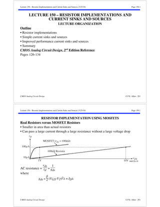
- 1. Lecture 150 – Resistor Implementations and Current Sinks and Sources (3/25/10) Page 150-1 LECTURE 150 – RESISTOR IMPLEMENTATIONS AND CURRENT SINKS AND SOURCES LECTURE ORGANIZATION Outline • Resistor implementations • Simple current sinks and sources • Improved performance current sinks and sources • Summary CMOS Analog Circuit Design, 2nd Edition Reference Pages 126-134 CMOS Analog Circuit Design © P.E. Allen - 201 Lecture 150 – Resistor Implementations and Current Sinks and Sources (3/25/10) Page 150-2 RESISTOR IMPLEMENTATION USING MOSFETS Real Resistors versus MOSFET Resistors • Smaller in area than actual resistors • Can pass a large current through a large resistance without a large voltage drop vDS 060526-10 iD 100μA 1V MOSFET (rds = 100kΩ) 100kΩ Resistor 10μA 10V AC resistance = vds id = 1 gds where gds 2 (VGS-VT)2 = ID CMOS Analog Circuit Design © P.E. Allen - 201
- 2. Lecture 150 – Resistor Implementations and Current Sinks and Sources (3/25/10) Page 150-3 MOS Diode as a Resistor AC and DC resistance: DC resistance = VDS ID = VT ID + 2 ID Small-Signal Load (AC resistance): + D vds - id S 060526-11 rds D = G D = G S S G + vgs gmvgs S - AC resistance = vds id = 1 gm+gds 1 gm where gm = (VGS-VT) = 2ID CMOS Analog Circuit Design © P.E. Allen - 201 Lecture 150 – Resistor Implementations and Current Sinks and Sources (3/25/10) Page 150-4 Use of the MOSFET to Implement a Floating Resistor In many applications, it is useful to implement a resistance using a MOSFET. First, consider the simple, single MOSFET implementation. RAB = L K’W(VGS-VT) VBias RAB A B A B Fig. 4.2-9 100μA 60μA 20μA -20μA -60μA -100μA VGS=2V VGS=3V VGS=4V VGS=5V VGS=10V VGS=9V VGS=8V VGS=7V VGS=6V -1V -0.6V -0.2V 0.2V 0.6V 1V Fig. 4.2-95 CMOS Analog Circuit Design © P.E. Allen - 201
- 3. Lecture 150 – Resistor Implementations and Current Sinks and Sources (3/25/10) Page 150-5 Cancellation of Second-Order Voltage Dependence – Parallel MOSFETs Circuit: M1 iAB iAB VC A B A RAB B M2 + - vAB Assume both devices are non-saturated iD1 = ß1 vAB2 2 (vAB+VC-VT)vAB- iD2 = ß2 vAB2 2 (VC-VT)vAB- iAB = iD1 + iD2 = ß + - vAB2 2 VC vAB2 2 +(VC-VT)vAB- vAB2+(VC-VT)vAB- iAB = 2ß(VC - VT)vAB RAB= 1 2ß(VC-VT) vAB 060526-12 CMOS Analog Circuit Design © P.E. Allen - 201 Lecture 150 – Resistor Implementations and Current Sinks and Sources (3/25/10) Page 150-6 Parallel MOSFET Performance Voltage-Current Characteristic: Vc=7V 2mA 1mA -1mA W=15u L=3u VBS=-5.0V 6V 5V 4V 3V -2 -1 0 1 2 VDS 0 I(VSENSE) -2mA Fig. 4.1-11 SPICE Input File: NMOS parallel transistor realization M1 2 1 0 5 MNMOS W=15U L=3U M2 2 4 0 5 MNMOS W=15U L=3U .MODEL MNMOS NMOS VTO=0.75, KP=25U, +LAMBDA=0.01, GAMMA=0.8 PHI=0.6 VC 1 2 E1 4 0 1 2 1.0 VSENSE 10 2 DC 0 VDS 10 0 VSS 5 0 DC -5 .DC VDS -2.0 2.0 .2 VC 3 7 1 .PRINT DC I(VSENSE) .PROBE .END CMOS Analog Circuit Design © P.E. Allen - 201
- 4. Lecture 150 – Resistor Implementations and Current Sinks and Sources (3/25/10) Page 150-7 SIMPLE CURRENT SINKS AND SOURCES Ideal Current Sinks and Sources What is an ideal current sink or source? v 060527-01 i Io + − v i Io • Current is fixed at a value of Io • Voltage can be any value from + to - • Be careful when using a current sink or source to replace a MOSFET sink/source in simulation CMOS Analog Circuit Design © P.E. Allen - 201 Lecture 150 – Resistor Implementations and Current Sinks and Sources (3/25/10) Page 150-8 Characterization of MOSFET Sinks and Sources A sink/source is characterized by two quantities: • rout - a measure of the “flatness” of the current sink/source (its independence of voltage) • VMIN - the min. across the sink or source for which the current is no longer constant NMOS Current Sink: VGG vDS = v 0601527-02 VDD VGG i v + - iDS= i VMIN VGG-VT0 Io 0 0 Slope = 1/rout VDD VDD Io i v + - rout = 1 diD/dvDS = 1+VDS D 1 ID and VMIN = VDS(sat) = VGS - VT0 = VGG - VT0 Note: The NMOS current sink can only have positive values of v. CMOS Analog Circuit Design © P.E. Allen - 201
- 5. Lecture 150 – Resistor Implementations and Current Sinks and Sources (3/25/10) Page 150-9 PMOS Current Source VGG vSD = v 0601527-03 VDD + VGG - Io i + - v iSD= i VMIN VGG-|VT0| 0 0 Slope = 1/rout VDD VDD Io i v CMOS Analog Circuit Design © P.E. Allen - 201 Lecture 150 – Resistor Implementations and Current Sinks and Sources (3/25/10) Page 150-10 Gate-Source Voltage Components It is important to note that the gate-source voltage consists of two parts as illustrated below: 10W/L W/L 0.1W/L vGS Provide Current Fig. 280-03 VT ID VGS iD 0 0 Enhance Channel VGS = VT0 + VON = Part to enhance the channel + Part to cause current flow where VON = VDS(sat) = VGS - VT0 VMIN=VON=VDS(sat)= 2ID K’(W/L) for the simple current sink. Note that VMIN can be reduced by using large values of W/L. CMOS Analog Circuit Design © P.E. Allen - 201
- 6. Lecture 150 – Resistor Implementations and Current Sinks and Sources (3/25/10) Page 150-11 Simulation of a Simple MOS Current Sink 120 100 80 60 40 20 0 Slope = 1/Rout Vmin VGS1 = 1.126V iOUT + vOUT - 10μm 1μm 0 1 2 3 4 5 iOUT (μA) vOUT (Volts) Comments: VMIN is too large - desire VMIN to approach zero, at least approach VCE(sat) Slope too high - desire the characteristic to be flat implying very large output resistance (KN’ = 110μA/V2, VT = 0.7Vand = 0.04V-1) rds = 250k CMOS Analog Circuit Design © P.E. Allen - 201 Lecture 150 – Resistor Implementations and Current Sinks and Sources (3/25/10) Page 150-12 How is VGG Implemented? The only voltage source assumed available is VDD. Therefore, VGG, can be implemented in many ways with the example below being one way. VDD i v R + - VBias=VGG + - 0601527-04 VDD VGG i v + - Better and more stable implementations of VGG will be shown later. CMOS Analog Circuit Design © P.E. Allen - 201
- 7. Lecture 150 – Resistor Implementations and Current Sinks and Sources (3/25/10) Page 150-13 IMPROVED PERFORMANCE CURRENT SINKS Improving the Performance of the Simple NMOS Current Sink The simple NMOS current sink shown previously had two problems. 1.) The value of VMIN may be too large. 2.) The output resistance (250k) was too small. How can the designer solve these problems? 1.) The first problem can be solved by increasing the W/L value of the NMOS transistor. VMIN = VON = VDS(sat) = 2ID K’(W/L) In the simulation shown previously, VMIN = 2·100μA 110μA/V2·10 = 0.426V We could decrease this to 0.1V with a W/L = 182. 2.) How can the small output resistance be increased? Answer is feedback. CMOS Analog Circuit Design © P.E. Allen - 201 Lecture 150 – Resistor Implementations and Current Sinks and Sources (3/25/10) Page 150-14 Blackman’s Formula for Finding the Resistance at a Port with Feedback† Blackman’s formula to find the resistance at a port X, is based on the following circuit: The resistance seen looking into port X is given as, Rx = Rx(k=0) 1+RR(portshorted) 1+RR(portopened) The return ratio, RR, is found by changing the dependent source to an independent source as shown: Therefore, the return ratio is defined as, RR = - vc vc' = - ic ic' The key is to find a feedback circuit that when we calculate the RR, it is non-zero when port X is shorted and zero when port X is opened. In this case, the resistance at port X is Rx = Rx(k=0)[1 + RR(port shorted)] † R.B. Blackman, “Effect of Feedback on Impedance,” Bell Sys. Tech.J., Vol. 23, pp. 269-277, October 1943. CMOS Analog Circuit Design © P.E. Allen - 201
- 8. Lecture 150 – Resistor Implementations and Current Sinks and Sources (3/25/10) Page 150-15 Identification of the Proper Type of Feedback For the port X, the circuit variables associated with the input port should be able to be expressed as, Input Variable to Port X = Signal variable to the circuit – Feedback variable where the variables can be voltage or current. 1.) Series feedback (variables are voltage): RR(Vx = 0) 0 RR(Ix = 0) = 0 (Vin is disconnected from Vfb) 2.) Shunt feedback (variables are current): RR(Vx = 0) = 0(Iin is disconnected from Ifb) RR(Ix = 0) 0 We see that for series feedback RR(port opened) will be zero and for shunt feedback that RR(port shorted) will be zero. CMOS Analog Circuit Design © P.E. Allen - 201 Lecture 150 – Resistor Implementations and Current Sinks and Sources (3/25/10) Page 150-16 Increasing the Output Resistance of the Simple Current Sink Choosing series feedback, we select the following circuit to boost the output resistance of the simple current sink: Assume that we can neglect the bulk effect and find the input resistance by 1.) small-signal analysis and 2.) return ratio method. 1.) Small-signal Analysis: vx = (ix + gmvs)rds + ixR vx = (ix + gmixR)rds + ixR = ix(1 + R + gmrdsR) Rx = vx ix = 1 + R + gmrdsR gmrdsR 2.) Return Ratio: Rx(k=0) = Rx(gm=0) = rds + R RR(vx = 0) = - vc vc' = gm rdsR rds+R
- 10. RR(ix = 0) = 0 Rx = (rds + R) 1+gm rdsR rds+R
- 12. = 1 + R + gmrdsR gmrdsR CMOS Analog Circuit Design © P.E. Allen - 201
- 13. Lecture 150 – Resistor Implementations and Current Sinks and Sources (3/25/10) Page 150-17 Cascode Current Sink Replacing R with the simple current sink leads to a practical implementation shown as: iOUT + vOUT - M2 M1 VGG2 VGG1 gm2vgs2 gmbs2vbs2 gm1vgs1 rds1 vgs1 =vg2 = vb2 = 0 Small signal output resistance: Noting that vgs1 = vg2 = vb2 = 0 and writing a loop equation we get, vout = (iout - gm2vgs2 - gmbs2vbs2)rds2 + rds1iout However, vgs2 = 0 - vs2 = -ioutrds1 and vbs2 = 0 - vs2 = -ioutrds1 Therefore, vout = iout[rds1 + rds2 + gm2rds1rds2 + gmbs2rds1rds2] or rout = vout iout = rds1 + rds2 + gm2rds1rds2 + gmbs2rds1rds2 gm2rds1rds2 rds2 iout + vout + vs2 - Fig. 280-11 A general principle is beginning to emerge: The output resistance of a cascode circuit R x (Common source voltage gain of the cascoding transistor) - CMOS Analog Circuit Design © P.E. Allen - 201 Lecture 150 – Resistor Implementations and Current Sinks and Sources (3/25/10) Page 150-18 Design of VGG1 and VGG2 vOUT(min) = VDS1(sat)+VDS2(sat) 060527-06 VGG2 VGG1 M2 + − VGS2 + VDS2 ≥VDS2(sat) − + − VDS1= VDS1(sat) 1.) VGG1 is selected to provide the desired current. M1 is assumed to be in saturation. 2.) VGG2 is selected to keep VDS1 as small as possible and still be in saturation. VGG2 = VDS1(sat) + VGS2 = VDS1(sat) + VT + VDS2(sat) If W1/L1 = W2/L2, then VGG2 = 2VDS(sat) + VT = 2VON + VT Thus, for the previous NMOS current sink, VGG2 would be equal to, VGG2 = 2(0.426) + 0.7 = 1.552V CMOS Analog Circuit Design © P.E. Allen - 201
- 14. Lecture 150 – Resistor Implementations and Current Sinks and Sources (3/25/10) Page 150-19 Simulation of the Cascode CMOS Current Sink Example Use the model parameters KN’=110μA/V2, VT = 0.7 and N = 0.04V-1 to calculate (a) the small-signal output resistance for the simple current sink if IOUT = 100μA and (b) the small-signal output resistance for the cascode current sink with IOUT = 100μA. Assume that all W/L values are 1. 120 100 80 60 40 20 Vmin 0 iOUT (μA) Slope = 1/Rout All W/Ls are 10μm/1μm VGG2 = 1.552V VGG1 = 1.126V iOUT + vOUT - Solution (a) Using = 0.04 V-1 and IOUT = 100μA gives rds1 = 250k = rds2. (b) Ignoring the bulk effect, we find that gm1 = gm2 = 469μS which gives rout = (250k)(469μS)(250k) = 29.32M. 0 1 2 3 4 5 vOUT (Volts) Fig. 280-12 CMOS Analog Circuit Design © P.E. Allen - 201 Lecture 150 – Resistor Implementations and Current Sinks and Sources (3/25/10) Page 150-20 High-Swing Cascode Current Sink This current sink achieves the smallest possible VMIN. Since VON = 2ID K’(W/L) , then if L/W of M4 is quadrupled, then VON is doubled. VMIN = 2VON. Example iOUT VMIN 0 2VON vOUT 060527-07 + vOUT - M2 + VT+VON - M1 1/1 1/1 VDD VDD M3 VT+2VON 1/1 1/4 M4 iOUT + VON - + VON - + - + - VT+VON Use the cascode current sink configuration above to design a current sink of 100μA and a VMIN = 1V. Assume the device parameters of Table 3.1-2. Solution With VMIN = 1V, choose VON = 0.5V. Assuming M1 and M2 are identical gives WL = 2·IOUT K’·VON 2 = 2·100x10-6 110x10-6x0.25 = 7.27 W1 L1 = W2 L2 = W3 L3 = 7.27 and W4 L4 = 1.82 CMOS Analog Circuit Design © P.E. Allen - 201
- 15. Lecture 150 – Resistor Implementations and Current Sinks and Sources (3/25/10) Page 150-21 Improved High-Swing Cascode Current Sink Because the drain-source voltages of the matching transistors, M1 and M3 are not equal, iOUT IREF. To circumvent this problem the cascode current sink shown is utilized: R1 R2 1/4 VDD VDD M4 + VT+2VON Note that the drain-source voltage of M1 and M3 are identical causing iOUT to be a replication of IREF. Design Procedure 1.) Since VMIN = 2VON = 2VDS(sat), let VON = 0.5VMIN. 2.) VON = 2IREF K’(W/L) W1 L1 = W2 L2 = - W3 L3 = M5 1/1 + VT - + - VON - W5 L5 M3 1/1 = 1/1 + VT+VON + - VT+VON 2IREF K’VON M2 M1 1/1 2 = + vOUT - - iOUT 060527-08 + VON - + VON - 8IREF K’VMIN 2 3.) W4 L4 = 2IREF K’(VGS4-VT)2 = 2IREF K’(2VON)2 = IREF 2K’VON 2 CMOS Analog Circuit Design © P.E. Allen - 201 Lecture 150 – Resistor Implementations and Current Sinks and Sources (3/25/10) Page 150-22 Signal Flow in Transistors The last example brings up an interesting and important point. This point is illustrated by the following question, “How does IREF flow into the M3-M5 combination of transistors since there is no path to the gate of M5?” Consider how signals flow in transistors: Output Only D G - + + + S + + Output Only C B - + + + E + + Fig. 4.3-12B Input Only Input Only Answer to the above question: As VDD increases (i.e. the circuit begins to operate), IREF cannot flow into the drain of M5, so it flows through the path indicated by the arrow to the gate of M3. It charges the stray capacitance and causes the gate-source voltage of M3 to increase to the exact value necessary to cause IREF to flow through the M3-M5 combination. VDD M5 M3 + - IREF VT +2VON Fig. 4.3-12A VGS3 CMOS Analog Circuit Design © P.E. Allen - 201
- 16. Lecture 150 – Resistor Implementations and Current Sinks and Sources (3/25/10) Page 150-23 Example 150-1 - Design of a Minimum VMIN Current Sink Assume IREF = 100μA and design a cascode current sink with a VMIN = 0.3V using the following parameters: VTO=0.7, KP=110U, LAMBDA=0.04, GAMMA=0.4, PHI=0.7 Solution From the previous equations, we get W1 W2 W3 W5 L1 = L2 = L3 = L5 = 8IREF K’VMIN2 = 8·100 110·(0.3V)2 = 80.8 and W4 L4 = IREF 2K’VON2 = 100 2·110·0.152 = 20.2 Simulation Results: 120 100 80 60 40 20 0 VMIN 0 1 2 3 4 5 vOUT(V) iOUT(μA) Fig. 290-06 Low Vmin Cascade Current Sink - Method No. 2 M1 5 1 0 0 MNMOS W=81U L=1U M2 2 3 5 5 MNMOS W=81U L=1U M3 4 1 0 0 MNMOS W=81U L=1U M4 3 3 0 0 MNMOS W=20U L=1U M5 1 3 4 4 MNMOS W=81U L=1U .MODEL MNMOS NMOS VTO=0.7 KP=110U +LAMBDA=0.04 GAMMA=0.4 PHI=0.7 VDD 6 0 DC 5V IIN1 6 1 DC 100U IIN2 6 3 DC 100U VOUT 2 0 DC 5.0 .OP .DC VOUT 5 0 0.05 .PRINT DC ID(M2) .END CMOS Analog Circuit Design © P.E. Allen - 201 Lecture 150 – Resistor Implementations and Current Sinks and Sources (3/25/10) Page 150-24 Self-Biased Cascode Current Sink† The VT + 2VON bias voltage is developed through a series resistor. Design procedure: Same as the previous except R = VON IREF = VMIN 2IREF For the previous example, R = 0.3V 2·100μA = 1.5k If the reference current is small, R can become large. IREF VDD VT+2VON R iOU + VON - VT+VON + M3 M4 M1 M2 VT - + VON - + VON - Fig. 290- † T.L. Brooks and A.L. Westwick, “A Low-Power Differential CMOS Bandgap Reference,” Proc. of IEEE Inter. Solid-State Circuits Conf., Feb. 1994, pp. 248-249. CMOS Analog Circuit Design © P.E. Allen - 201
- 17. Lecture 150 – Resistor Implementations and Current Sinks and Sources (3/25/10) Page 150-25 MOS Regulated Cascode Sink† iOUT + vOUT VDD M3 A M4 M5 M7 M6 IREF VO1 IREF M1 M2 IREF - Increasing vGS3 VGS3(norm) VDS3(sat) vDS3 Fig. 290-08 VGS3(max) iD3 VDS3(min) Comments: • Achieves very high output resistance by increasing the loop gain (return-ratio) due to the M4-M5 inverting amplifier. LG = gm3rds2 gm4 gds4+gds5 gm3rds2gm4rds4 2 If rds4rds5, then rout rds3gm3rds2gm4rds4 2 • M3 maintains “constant” current even though it is no longer in the saturation region. † E. Sackinger and W. Guggenbuhl, “A Versatile Building Block: The CMOS Differential Difference Amplifier,” IEEE J. of Solid-State Circuits, vol. SC-22, no. 2, pp. 287-294, April 1987. CMOS Analog Circuit Design © P.E. Allen - 201 Lecture 150 – Resistor Implementations and Current Sinks and Sources (3/25/10) Page 150-26 Regulated Cascode Current Sink - Continued Small signal model: Solving for the output resistance: iout = gm3vgs3 + gds3(vout-vgs4) But vgs4 = ioutrds2 and vgs3 G3=D4=D5 + - rds5 rds4 rds2 gm4vgs4 gm3vgs3 rds3 D2= S3= G4 + vgs4 - iout D3 S2 = G2= S4 Fig. 290-09 vgs3 = vg3 - vs3 = -gm4(rds4||rds5)vgs4 - vgs4 = -rds2[1 + gm4(rds4||rds5)]iout iout = -gm3rds2[1 + gm4(rds4||rds5)]iout + gds3vout - gds3rds2iout vout = rds3[1 + gm3rds2 + gds3rds2 + gm3rds2gm4(rds4||rds5)]iout rout = vout iout = rds3[1 + gm3rds2 + gds3rds2 + gm3rds2gm4(rds4||rds5)] rds3gm3rds2gm4(rds4||rds5) + vout - If IREF = 100μA, all W/Ls are 10μm/1μm we get rds = 0.25M and gm = 469μS which gives rout (0.25M)(469μS)(0.25M)(469μS)(0.125M) = 1.72G CMOS Analog Circuit Design © P.E. Allen - 201
- 18. Lecture 150 – Resistor Implementations and Current Sinks and Sources (3/25/10) Page 150-27 Can 1G Output Resistance Really be Achieved? No, because of substrate currents. Substrate currents are caused by impact ionization due to high electric fields cause an impact which generates a hole-electron pair. The electrons flow out the drain and the holes flow into the substrate causing a substrate current flow. Illustration: VG VT Polysilicon B S p+ Depletion Region n+ A n+ Free electron Fixed Atom p- substrate VD VDS(sat) Fig130-7 Free hole Maximum output resistance 500M-1G CMOS Analog Circuit Design © P.E. Allen - 201 Lecture 150 – Resistor Implementations and Current Sinks and Sources (3/25/10) Page 150-28 Model of Substrate Current Flow Substrate current: iDB = K1(vDS - vDS(sat))iDe-[K2/(vDS-vDS(sat))] where K1 and K2 are process-dependent parameters (typical values: K1 = 5V-1 and K2 = 30V) Schematic model: D G S iDB B Fig130-8 Small-signal model: gdb = iDB vDB = K2 IDB VDS-VDS(sat) 1nS This conductance will prevent the realization of high-output resistance current sinks/sources such as the regulated cascode current sink. CMOS Analog Circuit Design © P.E. Allen - 201
- 19. Lecture 150 – Resistor Implementations and Current Sinks and Sources (3/25/10) Page 150-29 Minimizing the VMIN of the Regulated Cascode Current Sink VMIN: Without the use of the VO1 battery shown, VMIN is pretty bad. It is, VMIN = VGS4 + VDS3(sat) = VT + 2VON Minimizing VMIN: If VO1 = VT , then VMIN = 2VON. This is accomplished by the following circuit: If VGS4A - VGS4B = VDS2(sat) = VON, then VMIN = 2VON VDD VDD VDD M3 ID4A IB M4A M4B + + VGS4AVGS4B - - IB M1 M2 + iOUT VDS2 vOUT IREF+IB - IREF +IB + - + VDS2 - Fig. 290-10 2ID4 KN’(W4A/L4A) - 2IB KN’(W4B/L4B) = 2IB+2IREF KN’(W2/L2 or ID4 W4A/L4A - IB W4B/L4B = IB+IREF W2/L2 A number of solutions exist. For example, let IB = IREF. This gives ID4A = 5.824IREF assuming all W/L ratios are identical. CMOS Analog Circuit Design © P.E. Allen - 201 Lecture 150 – Resistor Implementations and Current Sinks and Sources (3/25/10) Page 150-30 Example 150-2 - Design of a Minimum VMIN Regulated Cascode Current Sink Design a regulated cascode current sink for 100μA and minimum voltage of VMIN = 0.3V. Solution Let the W/L ratios of M1 through M5 be equal and let IB = 10μA. Therefore, 2·100μA VMIN = 0.3V = VON3 + VON2 = 110μA/V2(W/L) + 2·110μA 110μA/V2(W/L) = 2·100μA 110μA/V2(W/L) 1+ 1.1 Therefore, 0.3V = 2·100μA 110μA/V2(W/L)(2.049) WL = 2·100μA·2.0492 110μA/V20.32 = 84.8 85. With IB = 10μA, then ID4A = 10+ 110 2 = 186μA +5V +5V +5V 110μA 186μA 10μA M3 M4A M4B 85/1 85/1 10μA M1 M2 + iOUT 85/1 vOUT 110μA - 85/1 85/1 Fig. 290-11 CMOS Analog Circuit Design © P.E. Allen - 201
- 20. Lecture 150 – Resistor Implementations and Current Sinks and Sources (3/25/10) Page 150-31 Comparison of the MOS Cascode and Regulated Cascode Current Sink Close examination in the knee area reveals interesting differences. Simulation results: 110 105 100 95 90 85 80 MOS Cascode Regulated MOS Cascode BJT Cascode 0 0.1 0.2 0.3 0.4 0.5 vOUT (V) iOUT (μA) Fig. 290-12 Comments: • The regulated cascode current is smaller than the cascode current because the drain-source voltages of M1 and M2 are not equal. • The regulated cascode current sink has a smaller VMIN due to the fact that M3 can have a drain-source voltage smaller than VDS(sat) CMOS Analog Circuit Design © P.E. Allen - 201 Lecture 150 – Resistor Implementations and Current Sinks and Sources (3/25/10) Page 150-32 SUMMARY Summary of Both BJT and MOS Current Sinks/Sources Current Sink/Source rOUT VMIN Simple MOS Current Sink rds = 1 D VDS(sat) = VON Simple BJT Current Sink ro = VA C VCE(sat) 0.2V Cascode MOS gm2rds2rds1 2VON Cascode BJT Fro 2VCE(sat) Regulated Cascode Current Sink rds3gm3rds2gm4(rds4||rds5) VT +VON Minimum VMIN Regulated rds3gm3rds2gm4(rds4||rds5) VON Cascode Current Sink Resistor Implementations • MOSFET resistors may use less area than actual resistors • Linearity is the primary issue for MOSFET resistor realizations CMOS Analog Circuit Design © P.E. Allen - 201