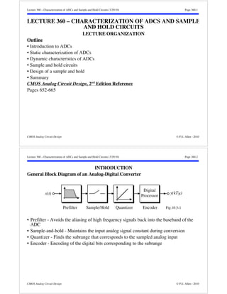
The document discusses characterization of analog-to-digital converters (ADCs) and sample and hold circuits. It introduces ADCs and their components. Static characterization of ADCs includes parameters like resolution, quantization noise, offset error, gain error, integral nonlinearity, and differential nonlinearity. Dynamic characteristics depend on comparators and sample/hold circuits. Sample/hold circuits must precisely sample signals within the clock period and hold the value for conversion. Open-loop sample/hold circuits are faster but less accurate than feedback circuits. Settling time calculations show higher resolution ADCs require more time for buffers to settle within accuracy limits.
Using Distortion Shaping Technique to Equalize ADC THD Performance Between ATEsPete Sarson, PH.D
This paper describes how using a phase switching technique can produce a low distortion signal from an Arbitrary Waveform Generator (AWG), and how this technique aligns the performance of the AWGs between testers, to evaluate the Total Harmonic Distortion (THD) performance of Analogue-to-Digital Converters (ADCs). Once a device has been characterized and correlated to the bench, the test engineer needs to start the release procedure in getting the device into a production ready state. One major issue that a test engineer faces is the difference in ADC THD performance test results using the same Automated Test Equipment (ATE) manufacture testers (AWGs). This paper will then show how the Gauge Repeatability and Reproducibility (GRR) between testers can be produced more easily allowing less stringent guard-bands to guarantee the performance of those devices that have performance criteria close to the device specification. This work will also go some way to proving previous papers’ works on distortion shaping testing to enhance the spectral performance of Arbitrary Waveform Generators.
Sonora DIRECTV TAMP6-T12 6-input Satellite Trunk Amplier wtih Auto GainWired At Home, LLC
The Sonora DIRECTV TAMP6-T12 6-Input Trunk Amp provides an automatic gain controlled output that is user adjustable from -15dBm to -24dBm at 2150 MHz. The Slope if field selected from either 12dB or 8dB.
http://www.wiredathome.com/satellite-tv-accessories/satellite-amplifiers/sonora-tamp6-t12-directv-6-input-trunk-amplifier-with-power-supply/
A 420uW 100GHz-GBW CMOS Programmable-Gain Amplifier Leveraging the Cross-Coup...aiclab
Cross-coupled pairs are certainly among the most widely adopted fundamental circuits still in use today. This elegant device arrangement yields broadband positive feedback with high gain and low power, desirable features both in analog and digital applications [1]. Its small signal properties are consistently leveraged in oscillators, impedance negators and to boost gain of transconductors, while the bistable behavior is exploited in static latches and memory cells. Traditionally, the regeneration capability is leveraged in the design of sense amplifiers and high-speed comparators. In this work, we investigated the performance of the cross-coupled pair for discrete-time linear amplification and we show that its regeneration feature proves to be attractive for implementing Programmable-Gain Amplifiers (PGAs).
Study and implementation of comparator in cmos 50 nm technologyeSAT Journals
Abstract This paper describes the comparator circuits used in FLASH Analog to digital converter (ADC). The performance of FLASH ADC is greatly influenced by the choice of comparator. In this paper, first a single ended “Threshold Inverter Quantizer” (TIQ) is presented. The TIQ comparator is based on a CMOS inverter cell, in which voltage transfer characteristics (VTC) are changed by systematic transistor sizing. However, TIQ comparator is very sensitive to power supply noise. Another comparator circuit presented in this paper is “Two stage open loop comparator”. It is implemented in 50 nm CMOS Technology. Pre-simulation of comparator is done in LT-Spice and post layout simulation is done in Microwind 3.1. Keywords: CMOS, Comparator, TIQ (Threshold Inverter Quantizer), LT-Spice.
Analog-to-Digital Converter (ADC) is an integral part of high-speed signal processing applications. This paper discusses about 10-bit SAR based ADC that enables very low power consumption and sampling rate as high as 165 MSPS.
A NEW APPROACH TO DESIGN LOW POWER CMOS FLASH A/D CONVERTERVLSICS Design
In the present paper, a 4-bit flash analog to digital converter for low power SoC application is presented. CMOS inverter has been used as a comparator and by adjusting the ratio of channel width and length, the switching threshold of the CMOS inverter is varied to detect the input analog signal. The simulation results show that this proposed 4-bit flash ADC consumes about 12.4 mW at 200M sample/s with 3.3V supply voltage in TSMC 0.35 µm process. Compared with the traditional flash ADC, this proposed method can reduce about 78% in power consumption.