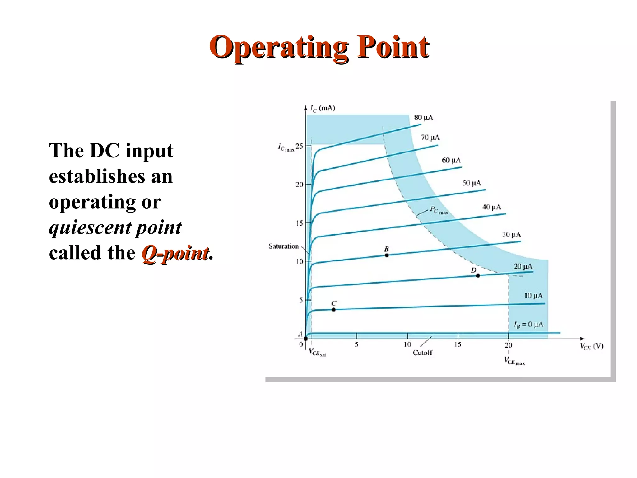
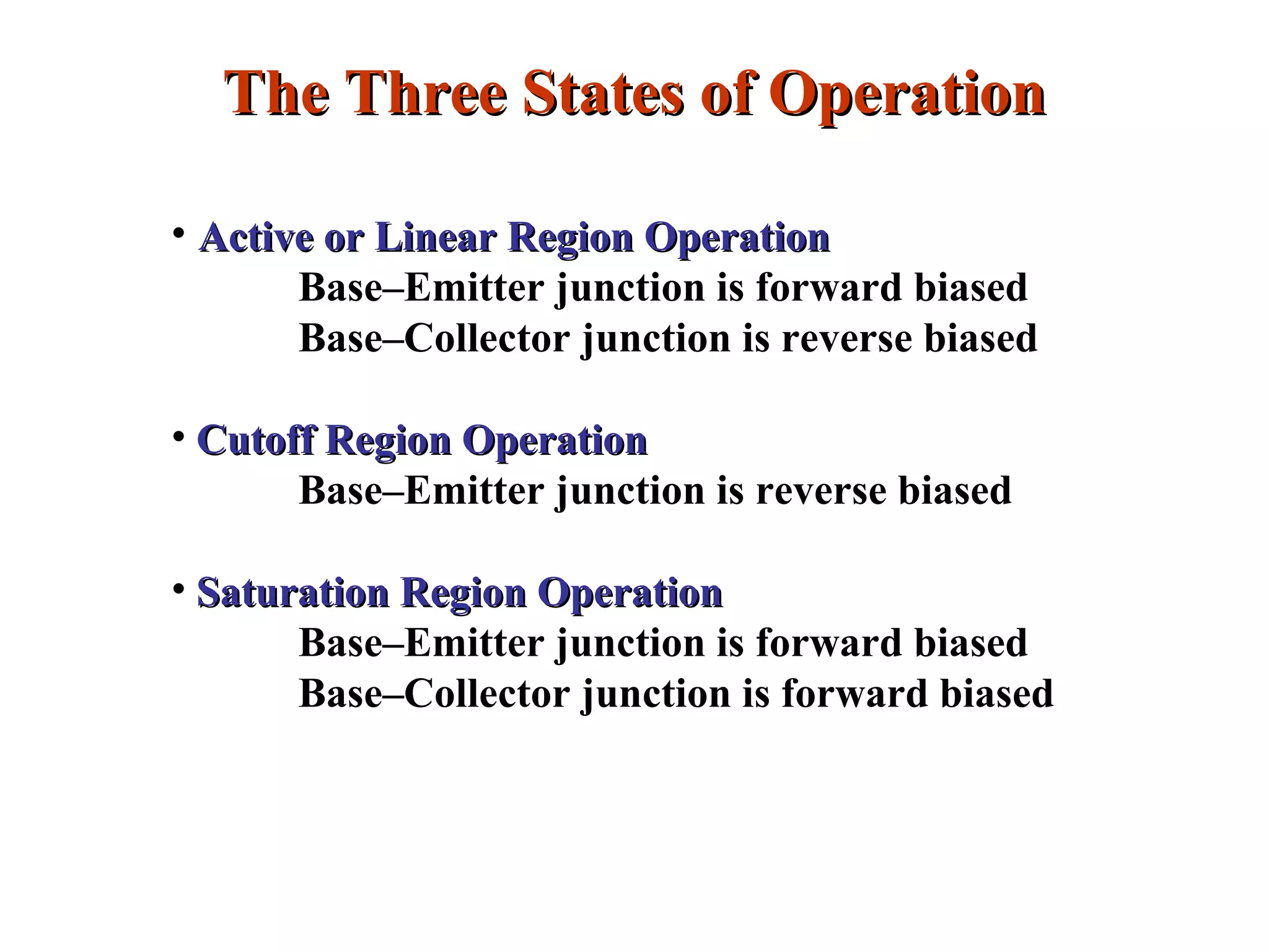
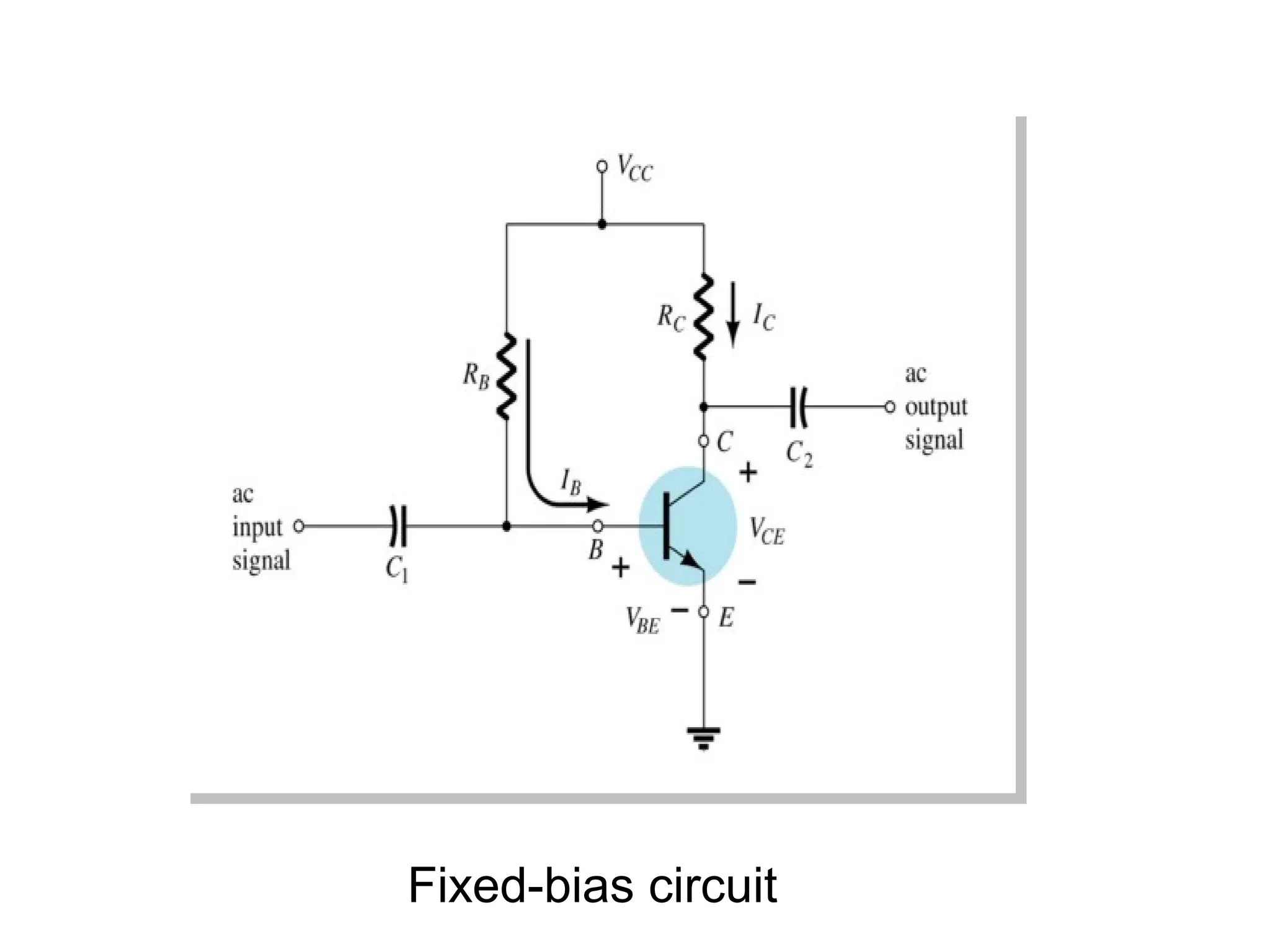
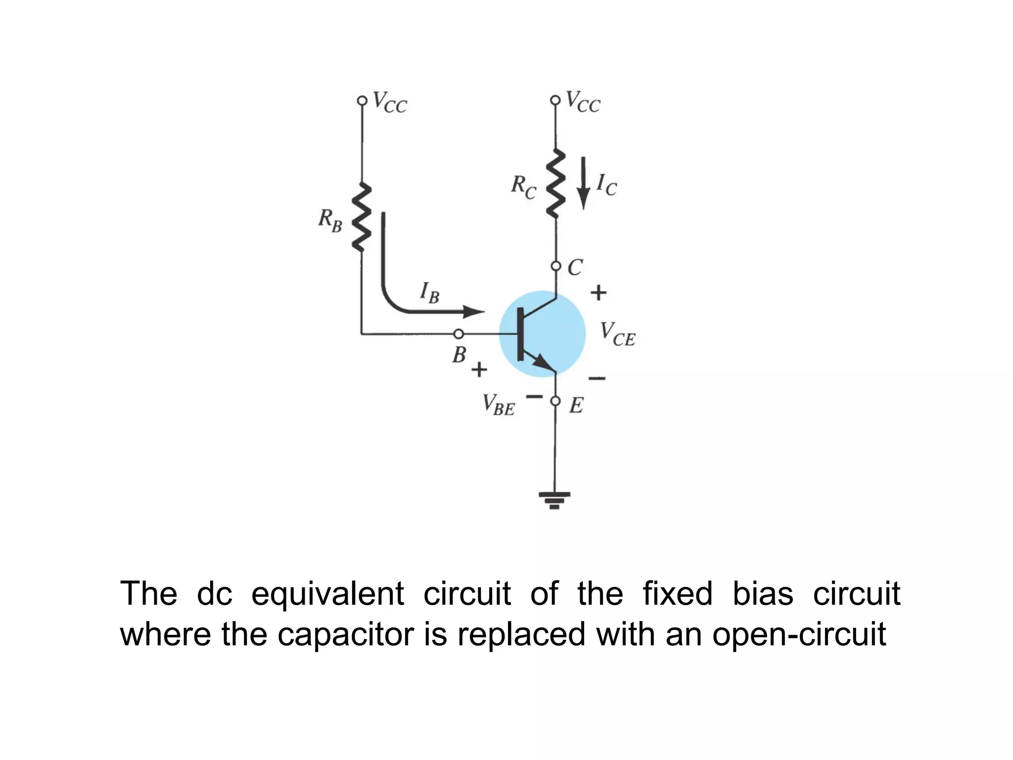
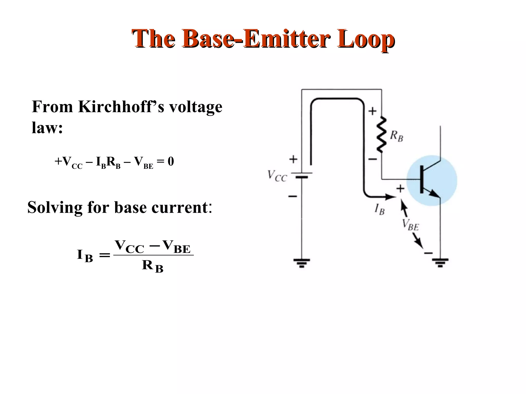
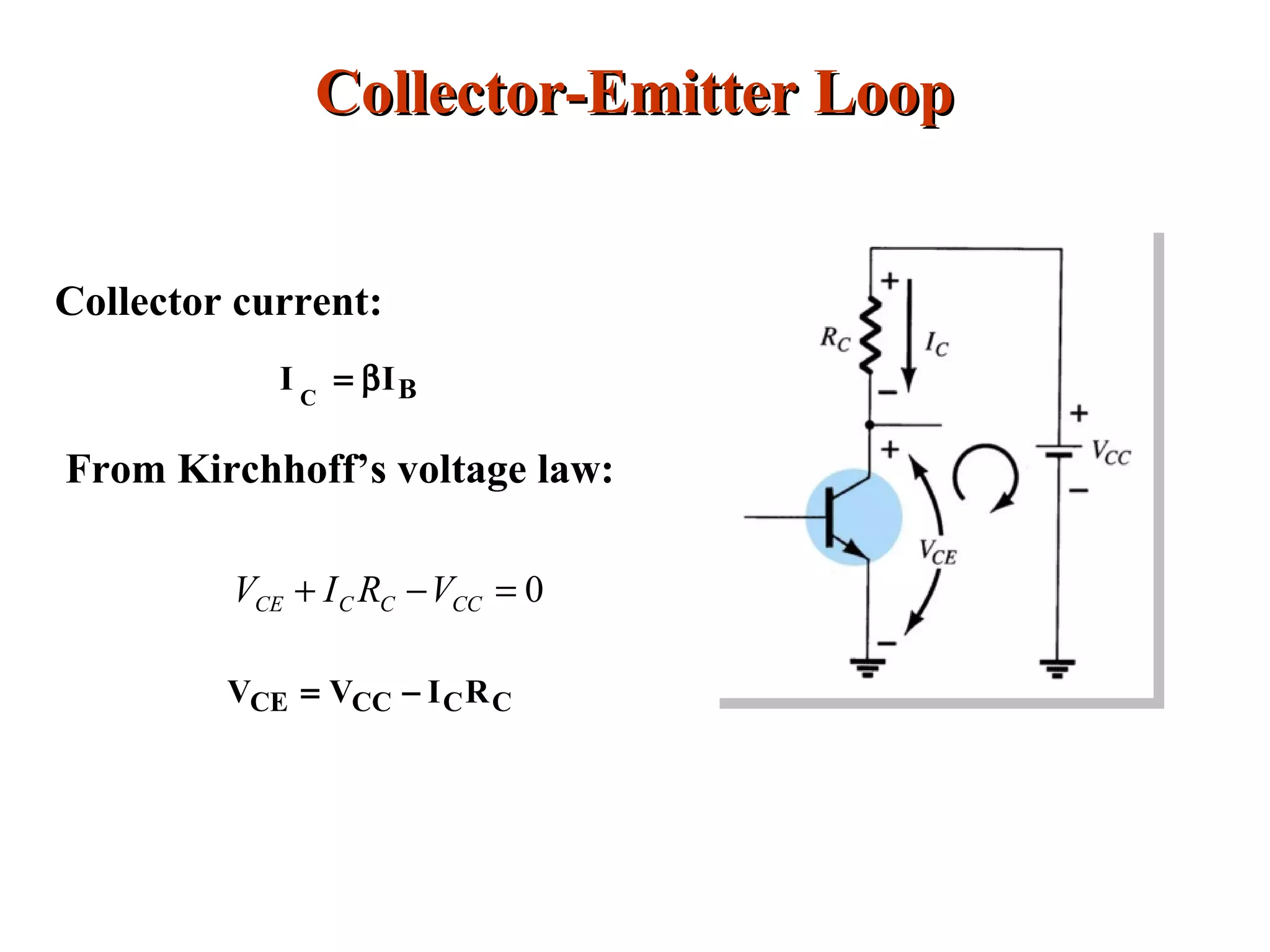
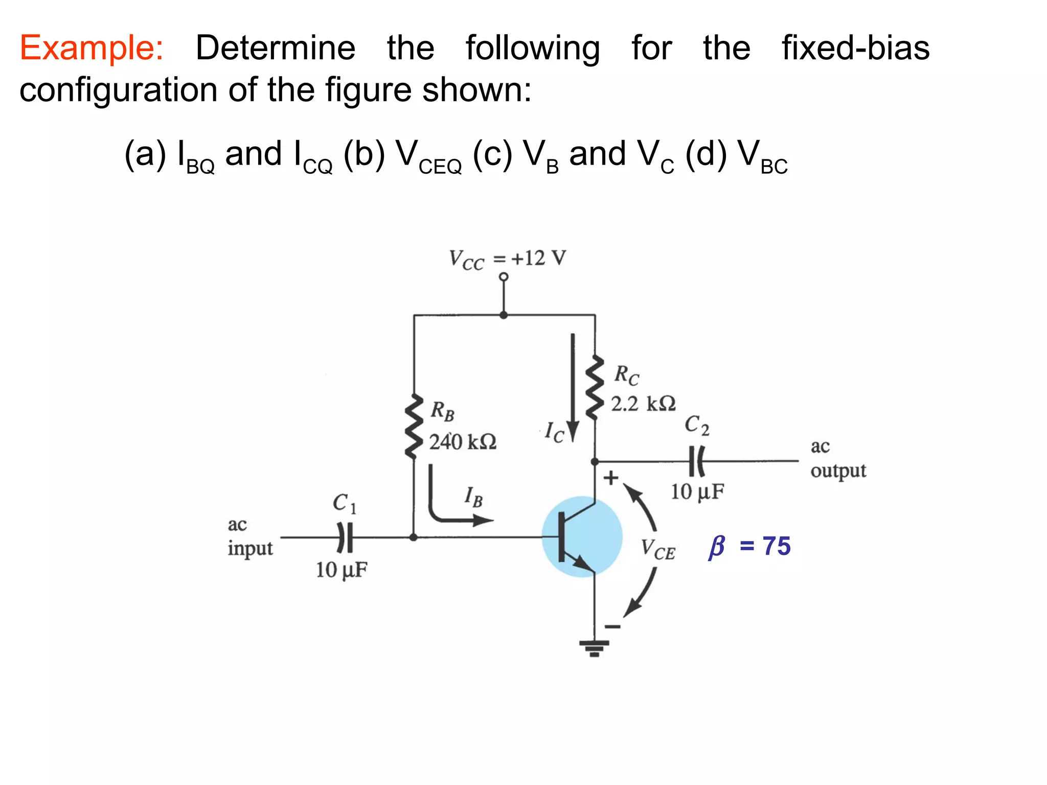
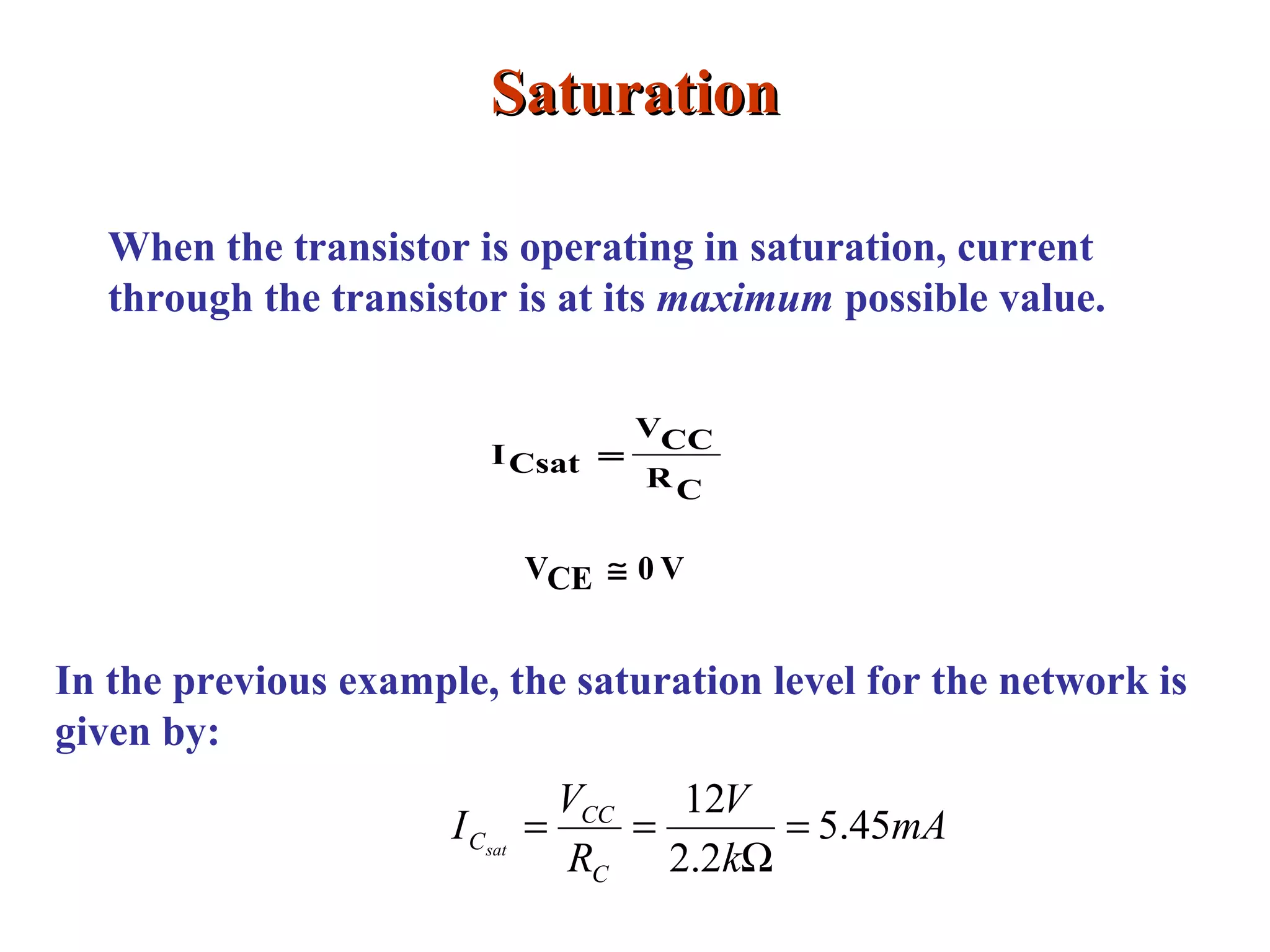
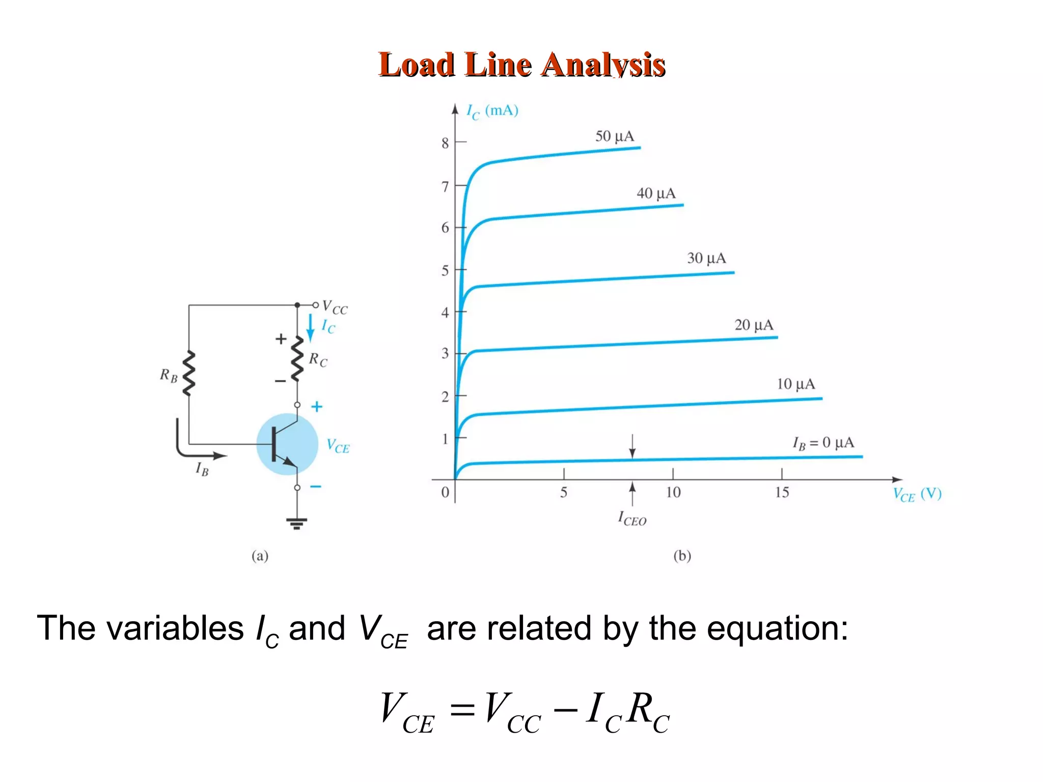
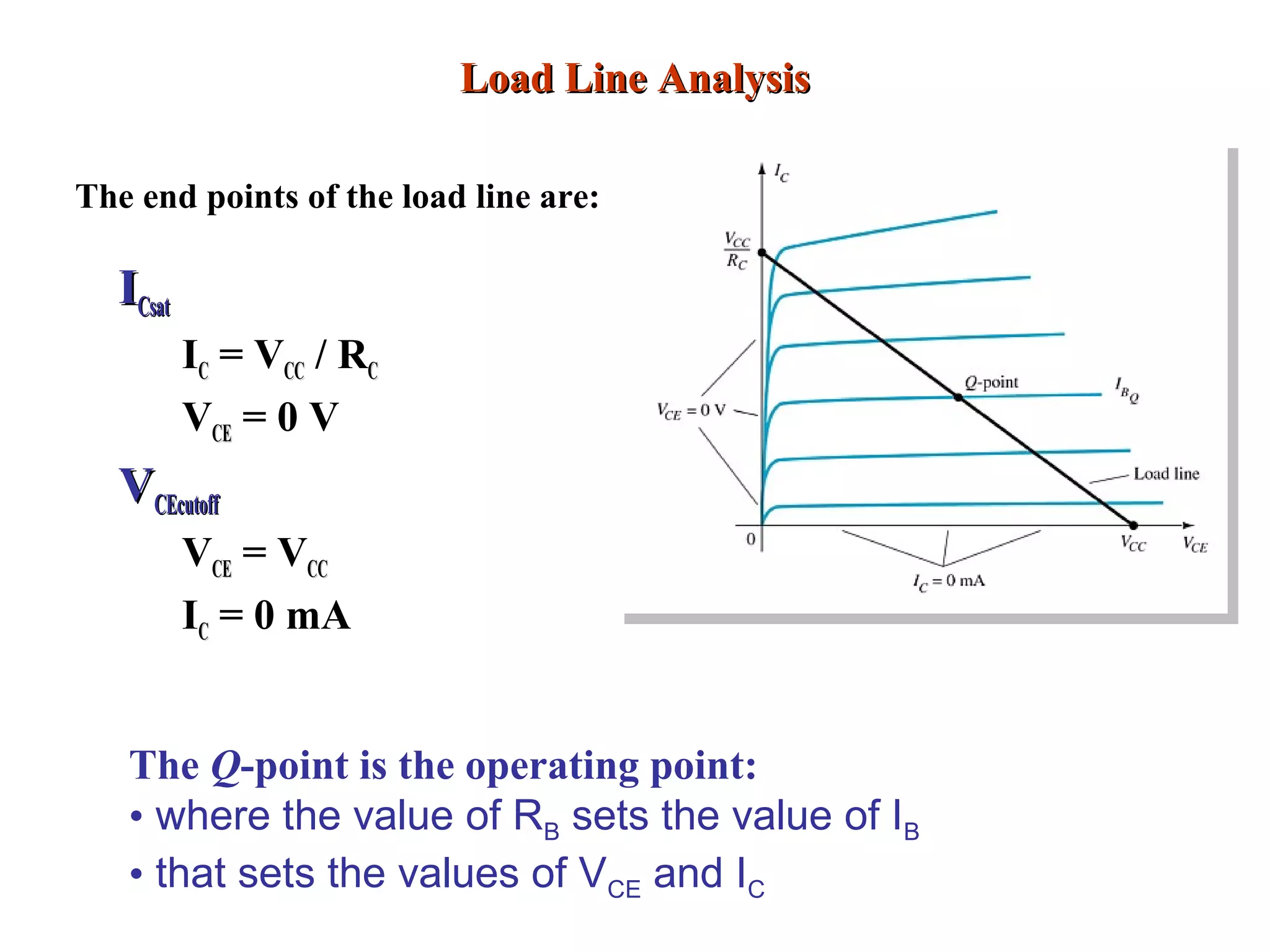
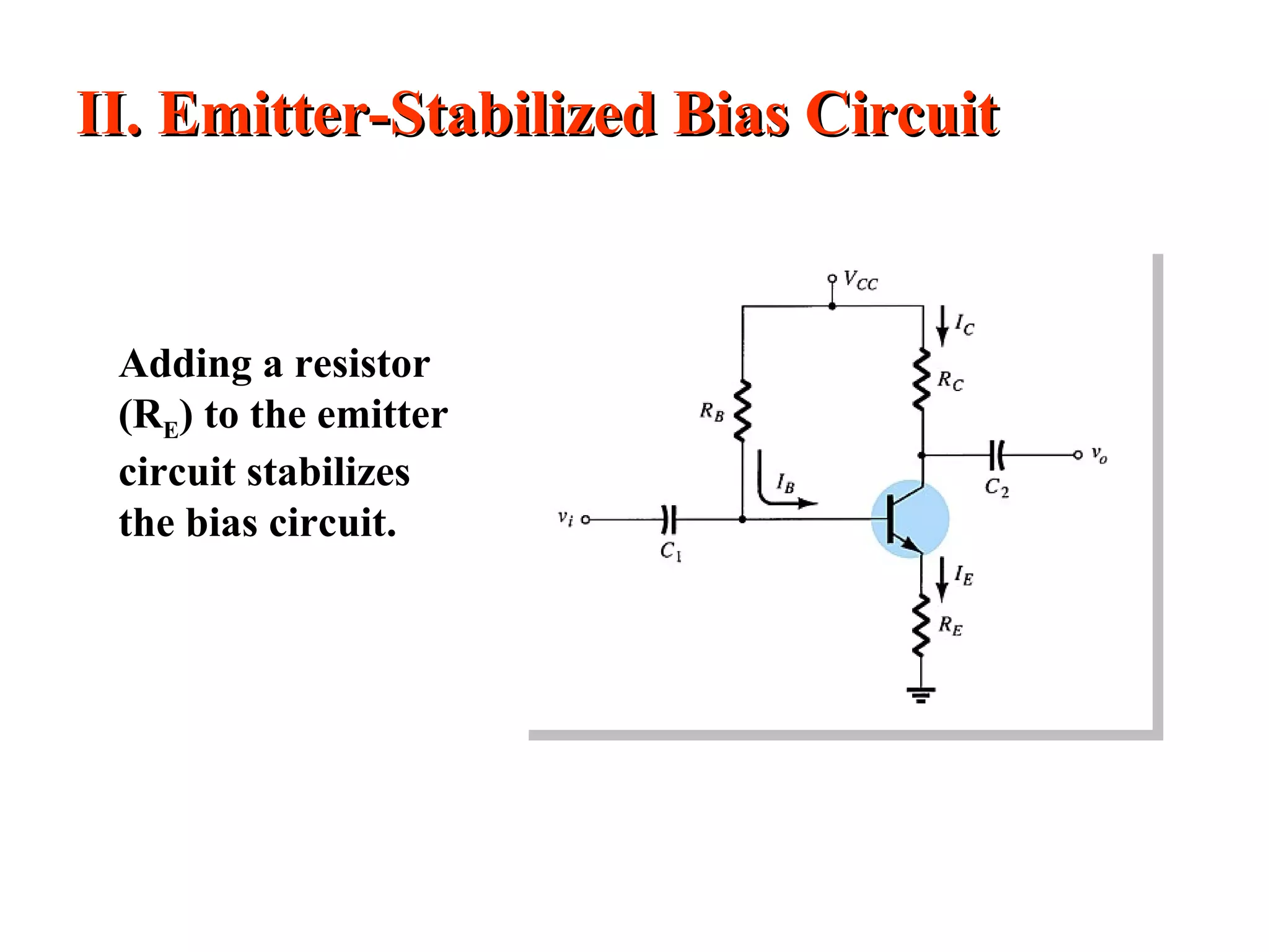
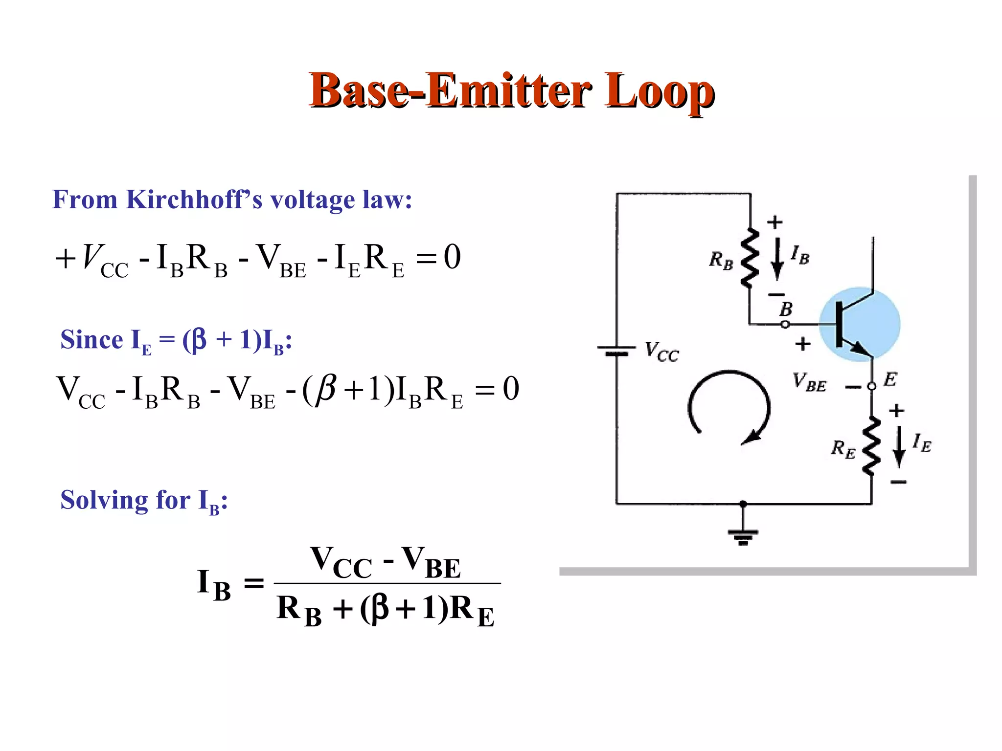
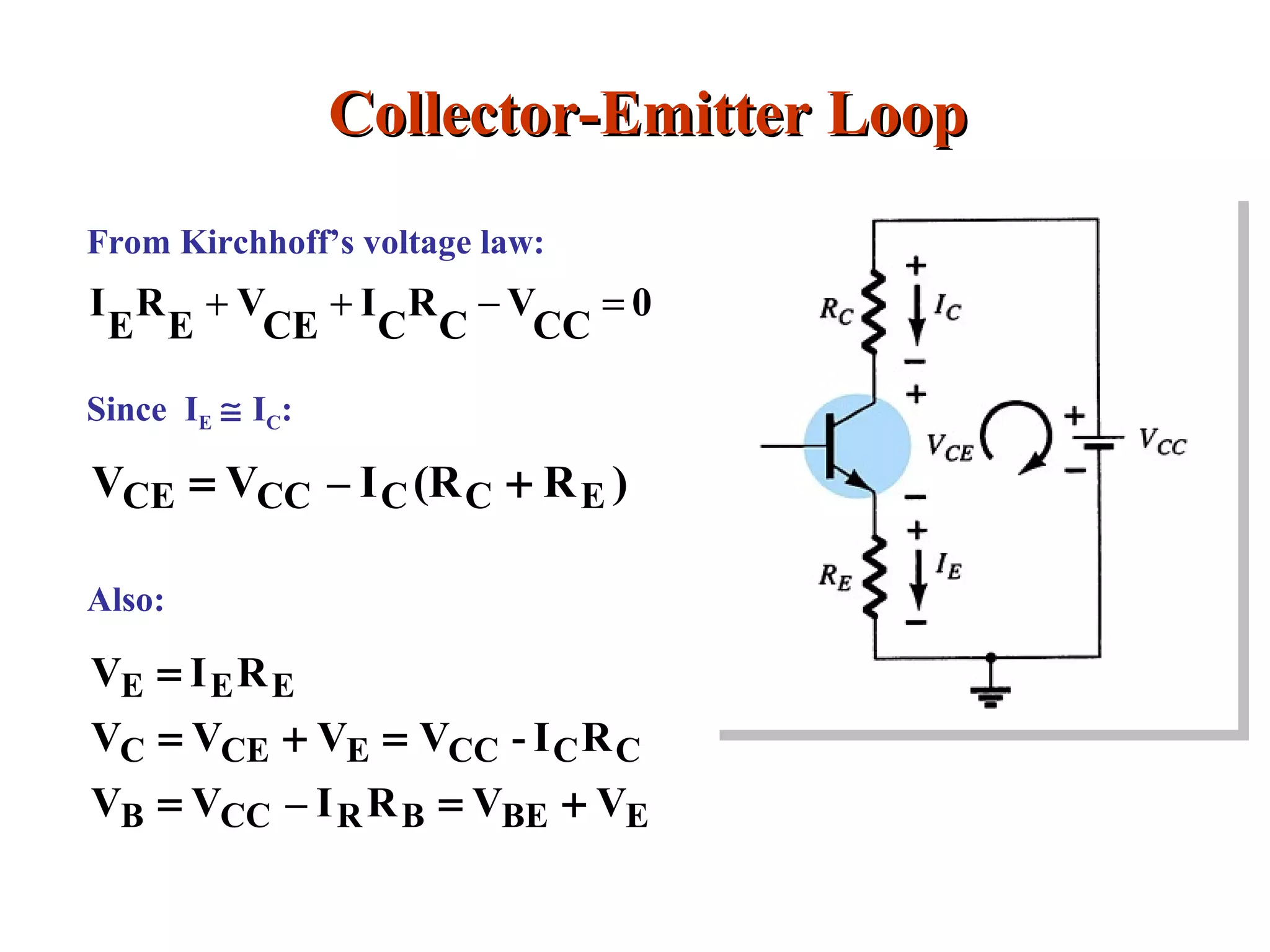
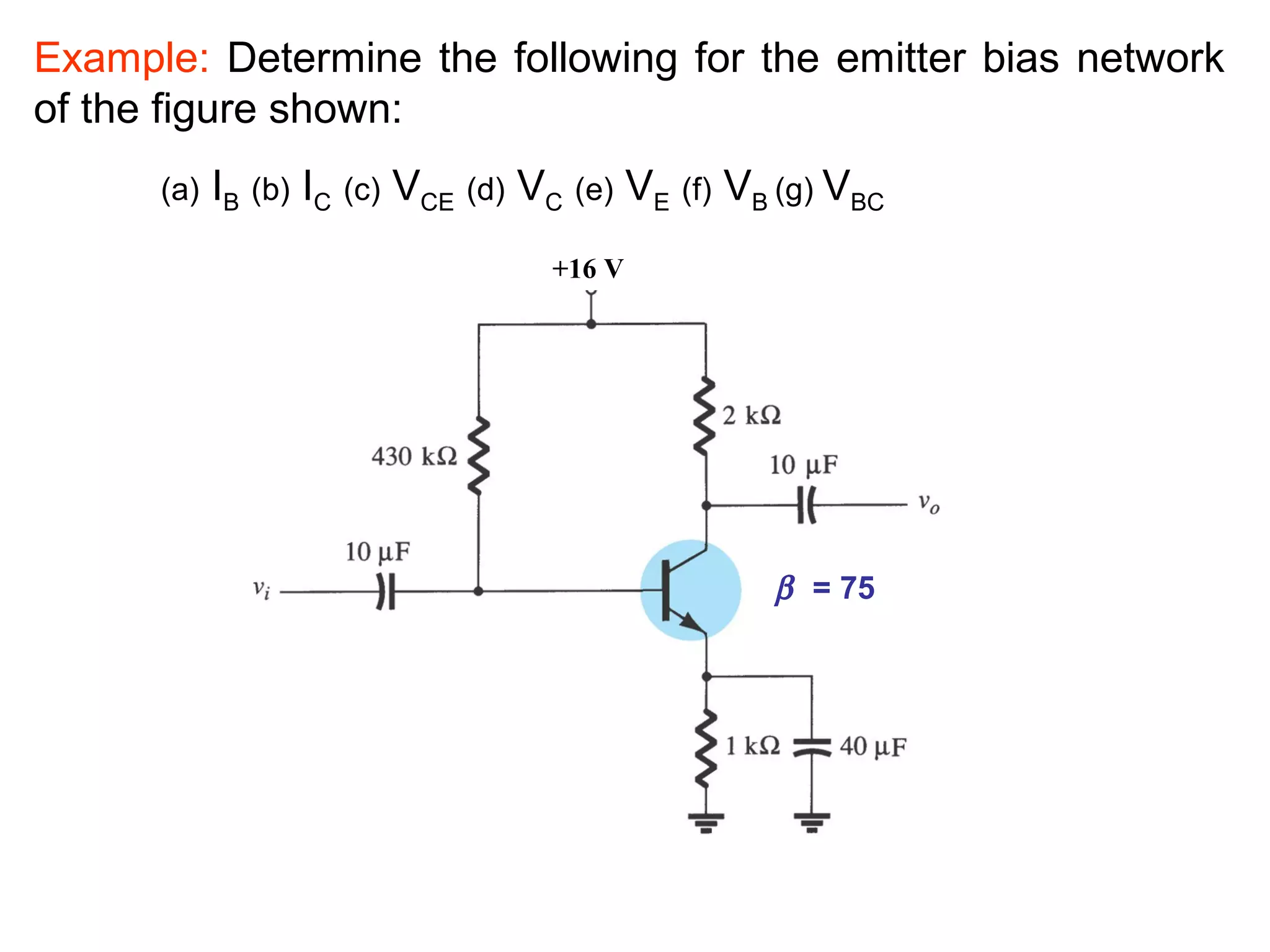
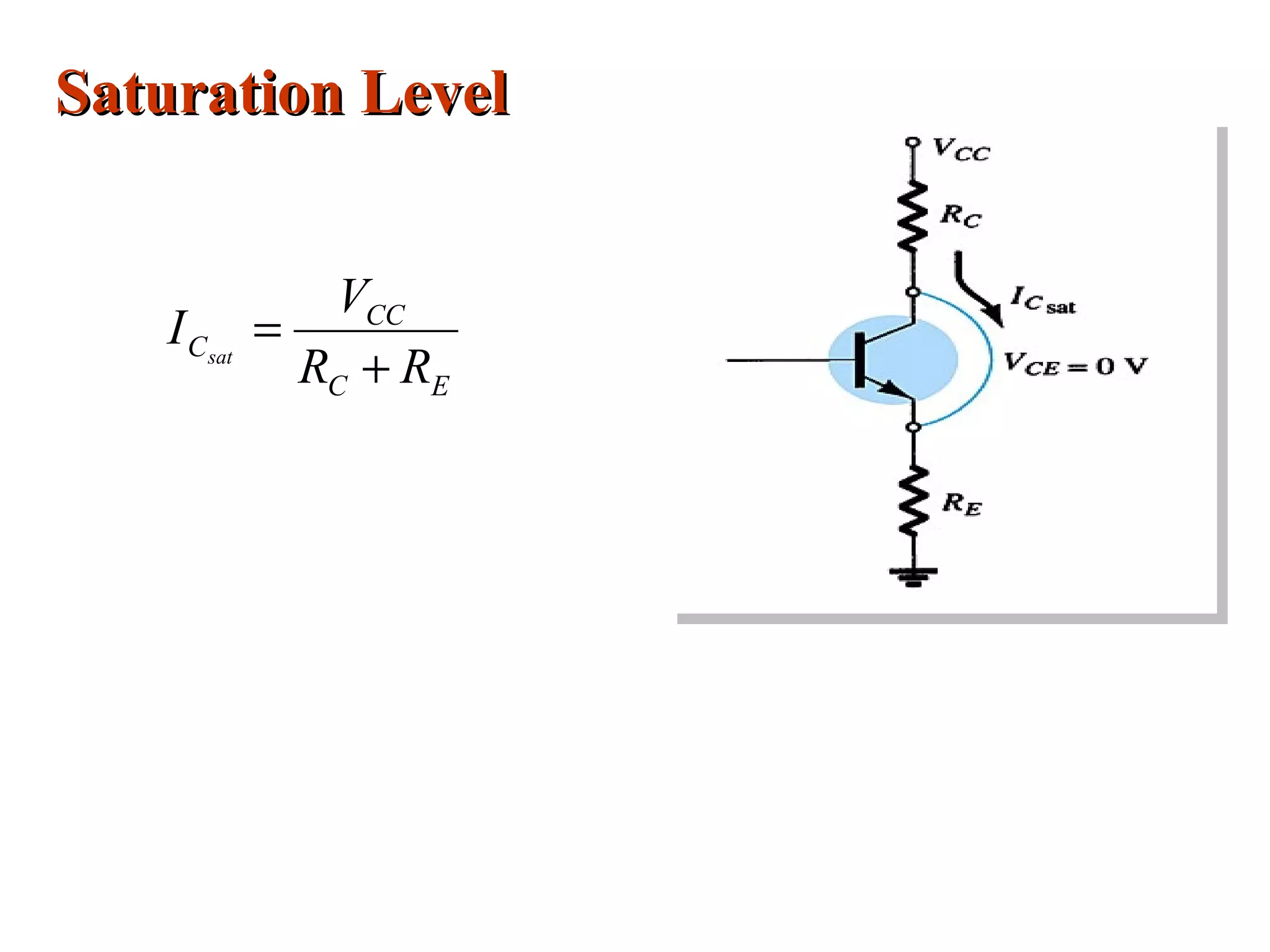
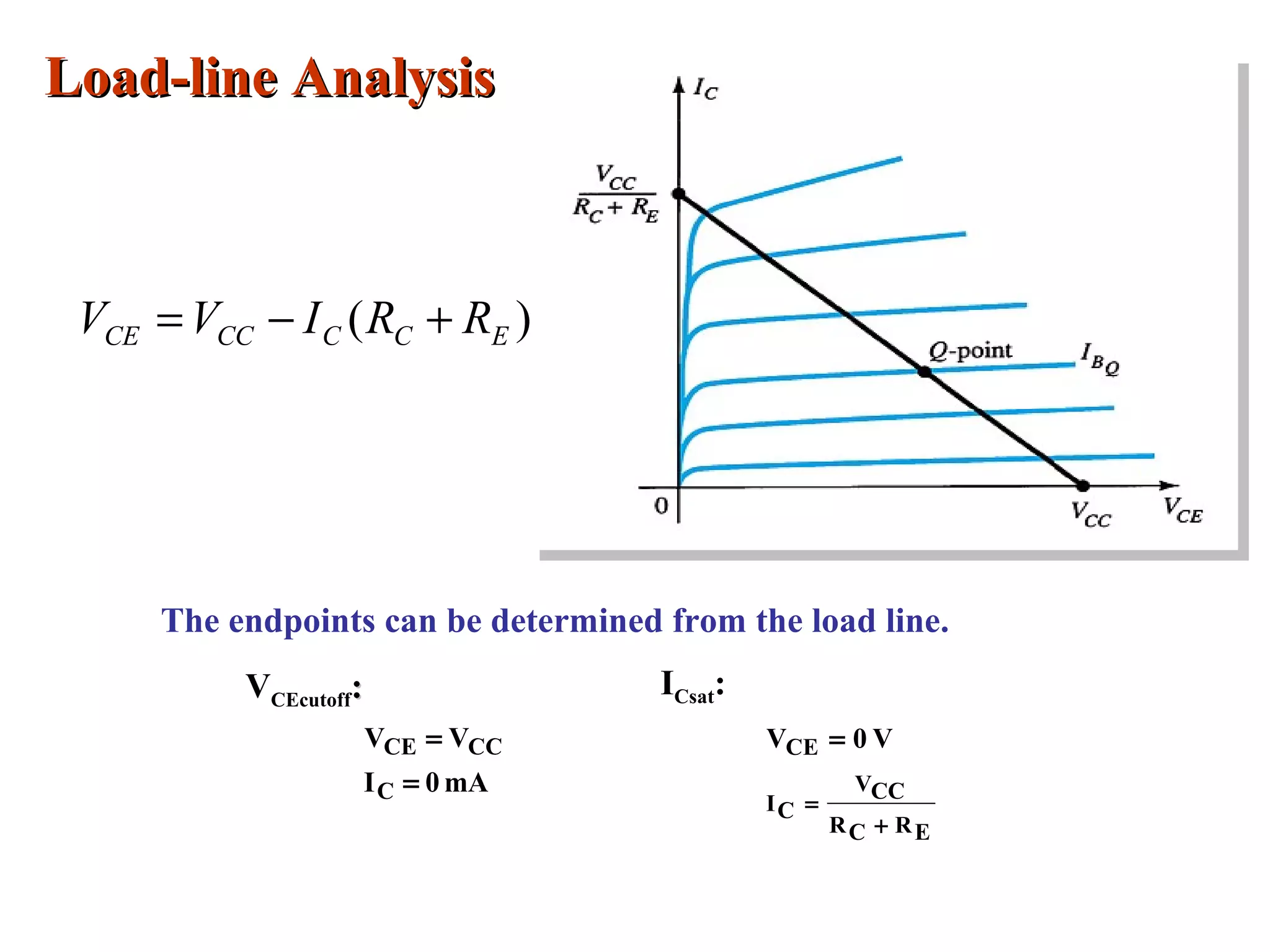
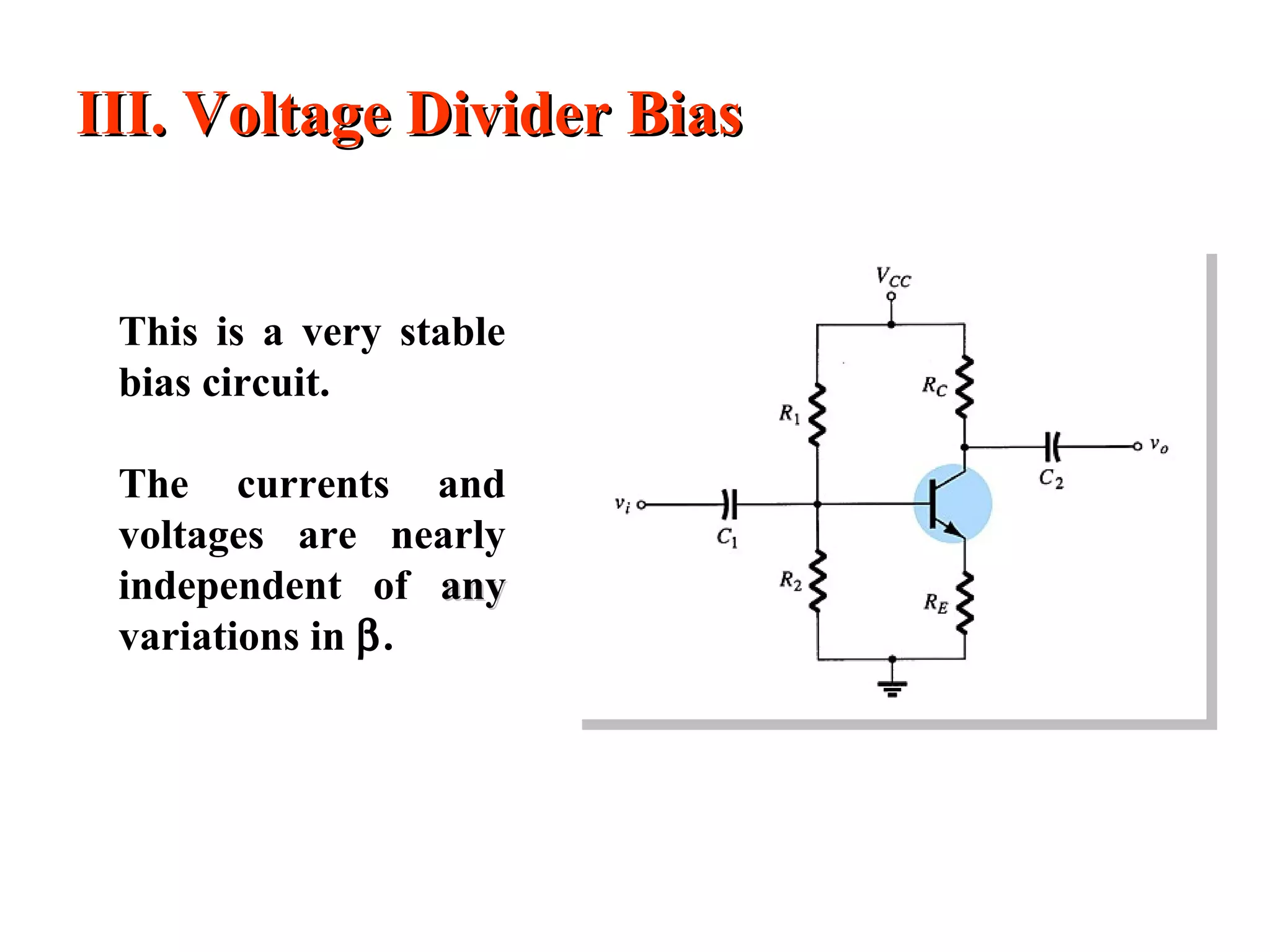
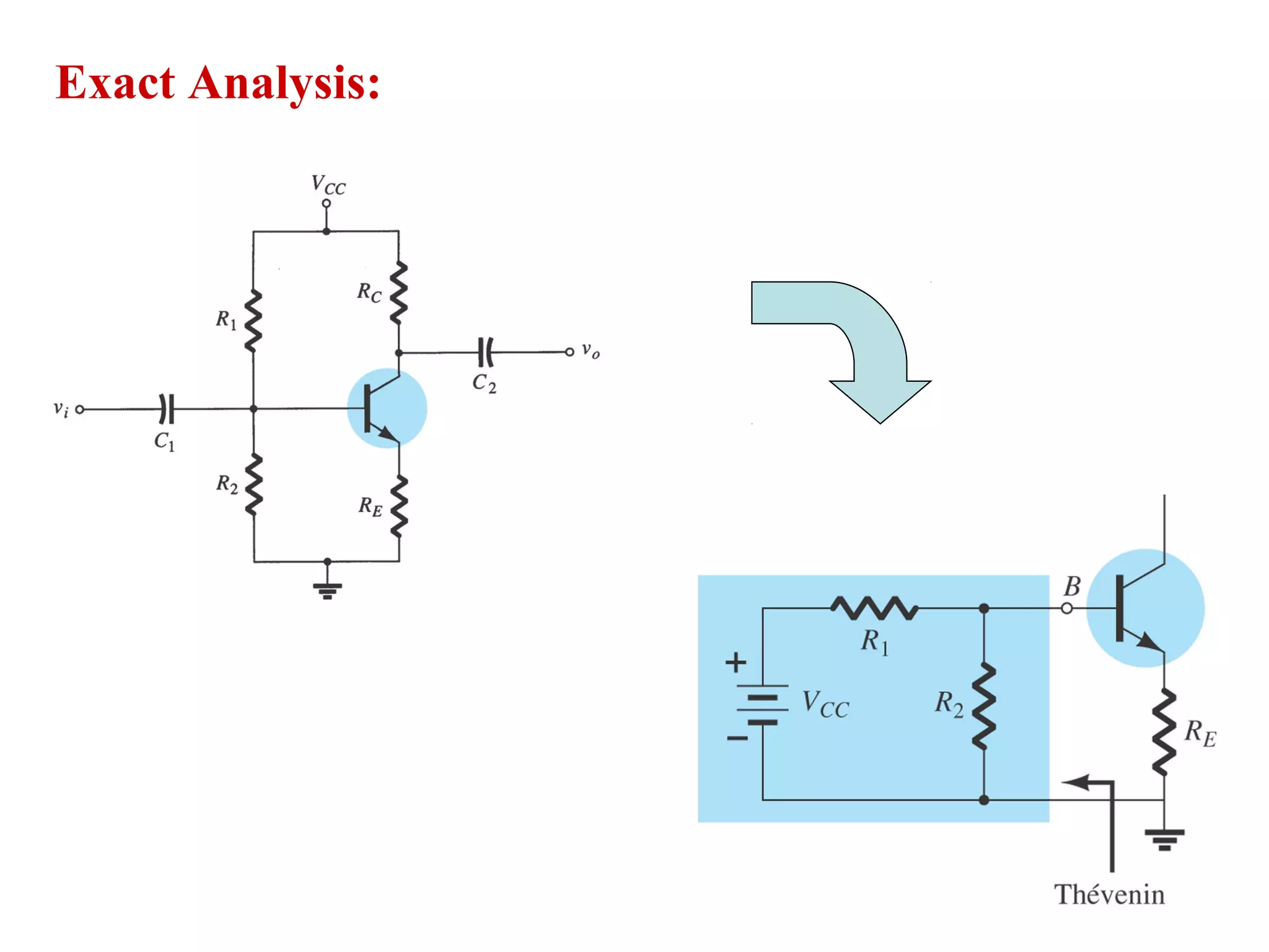
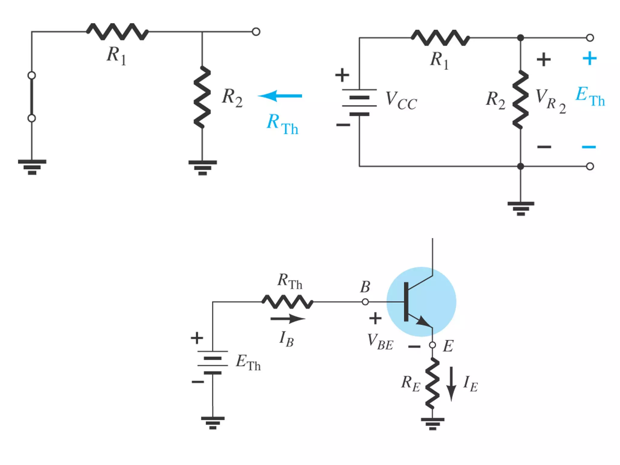
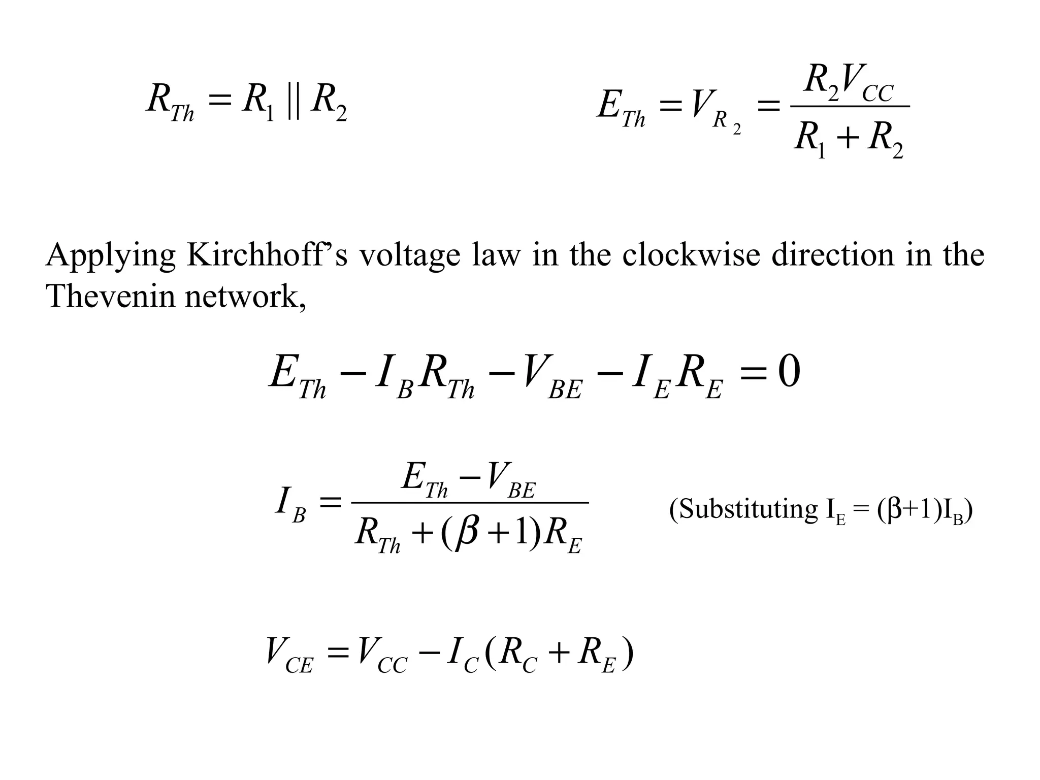
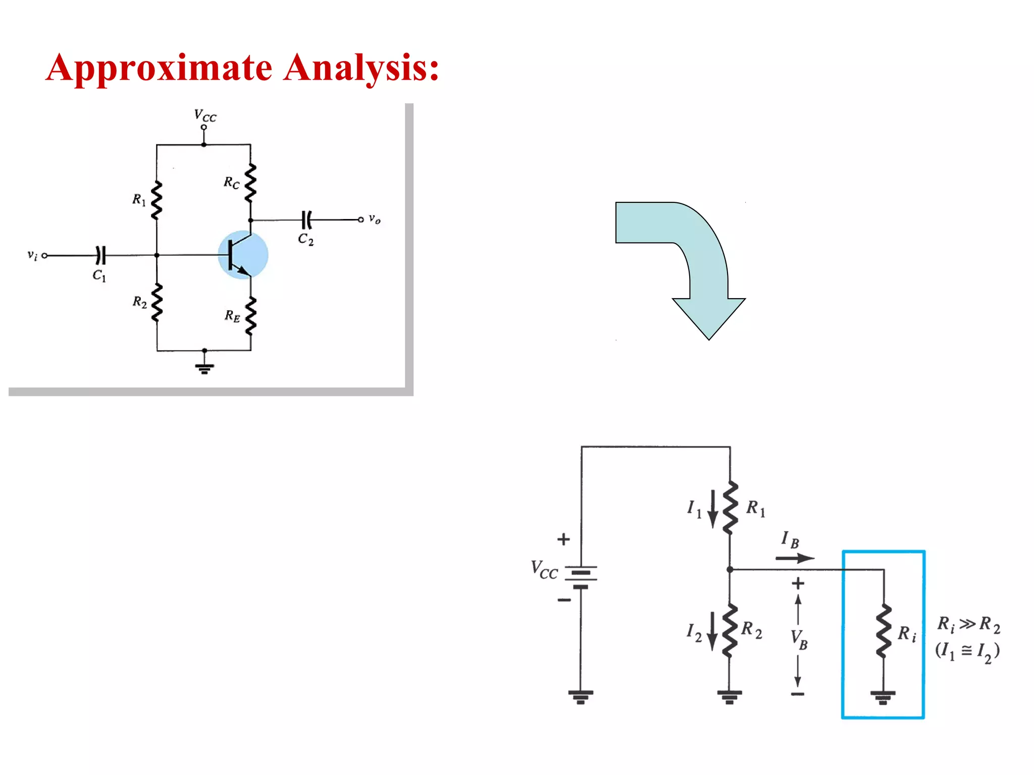
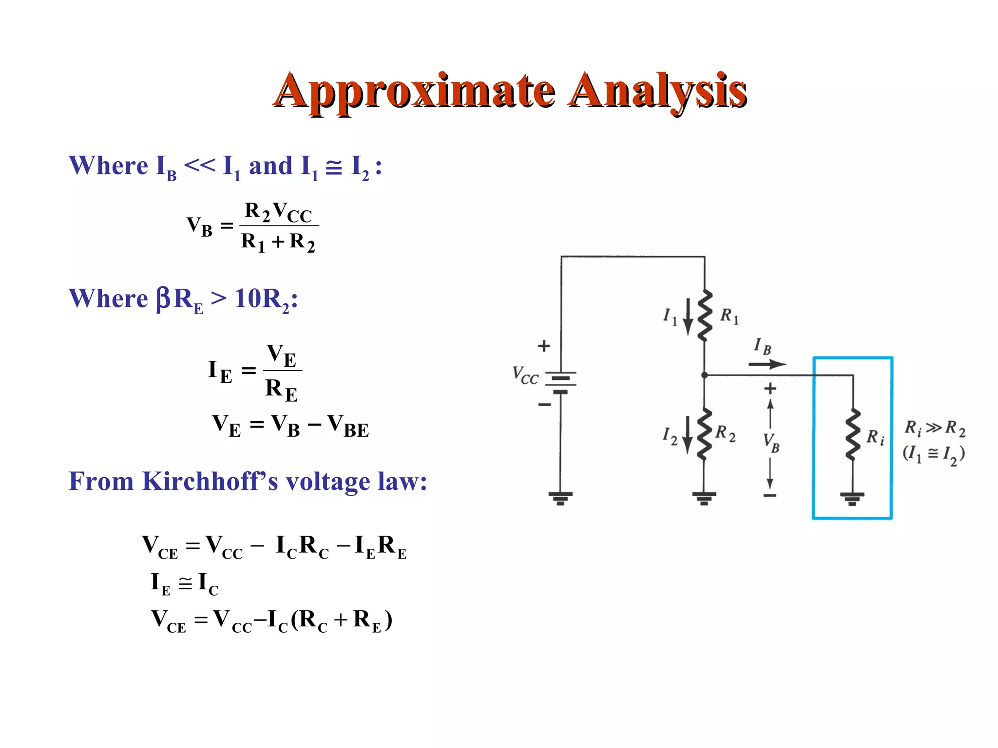
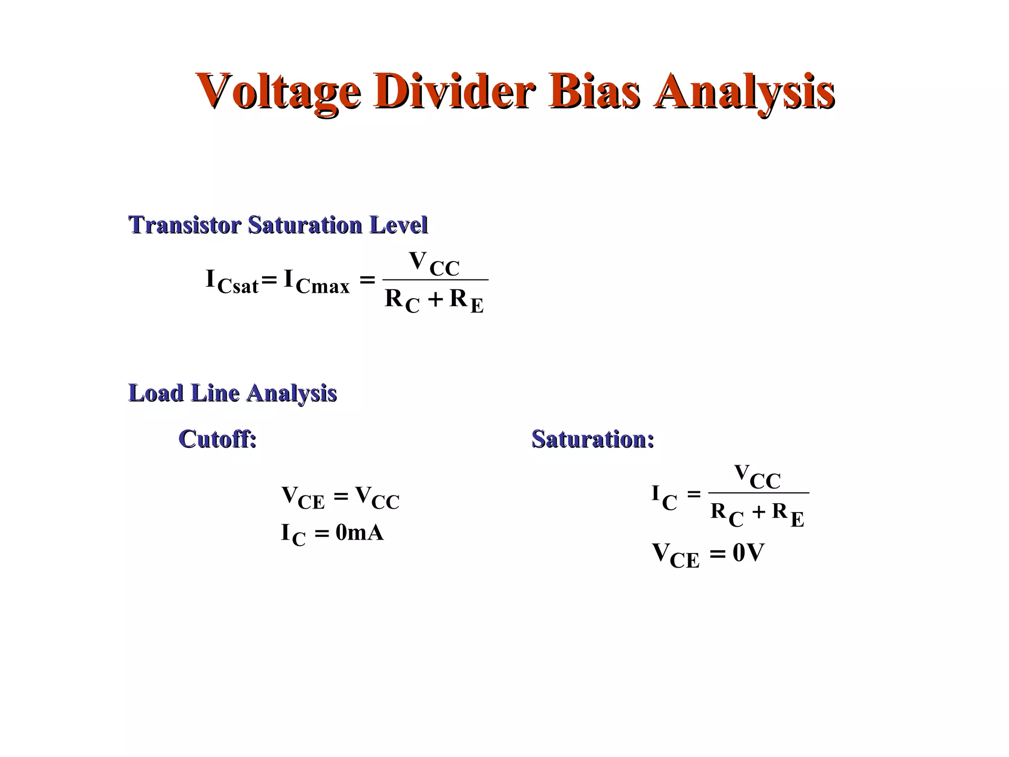
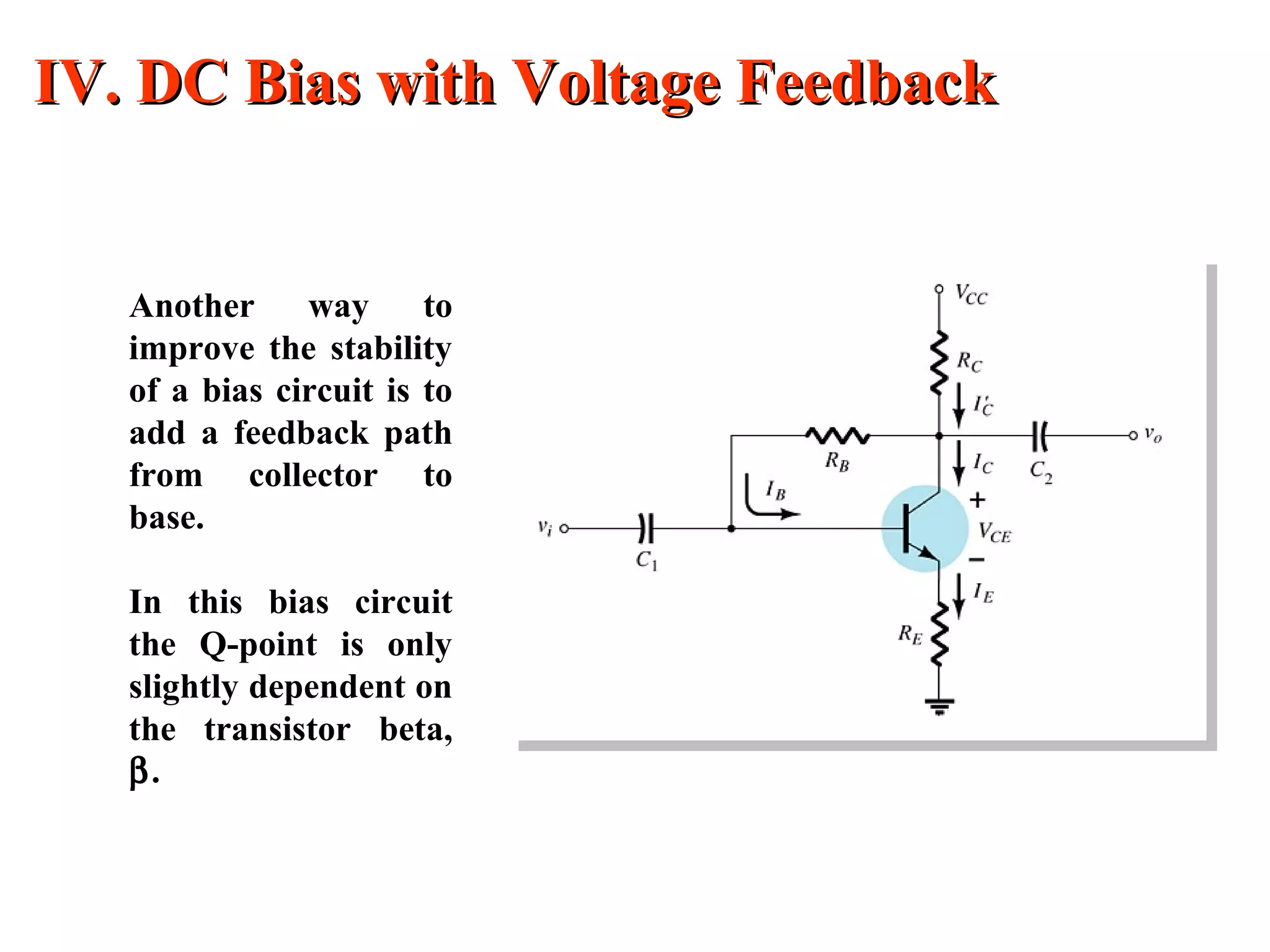
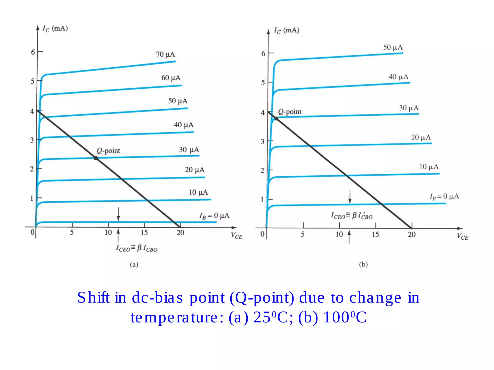
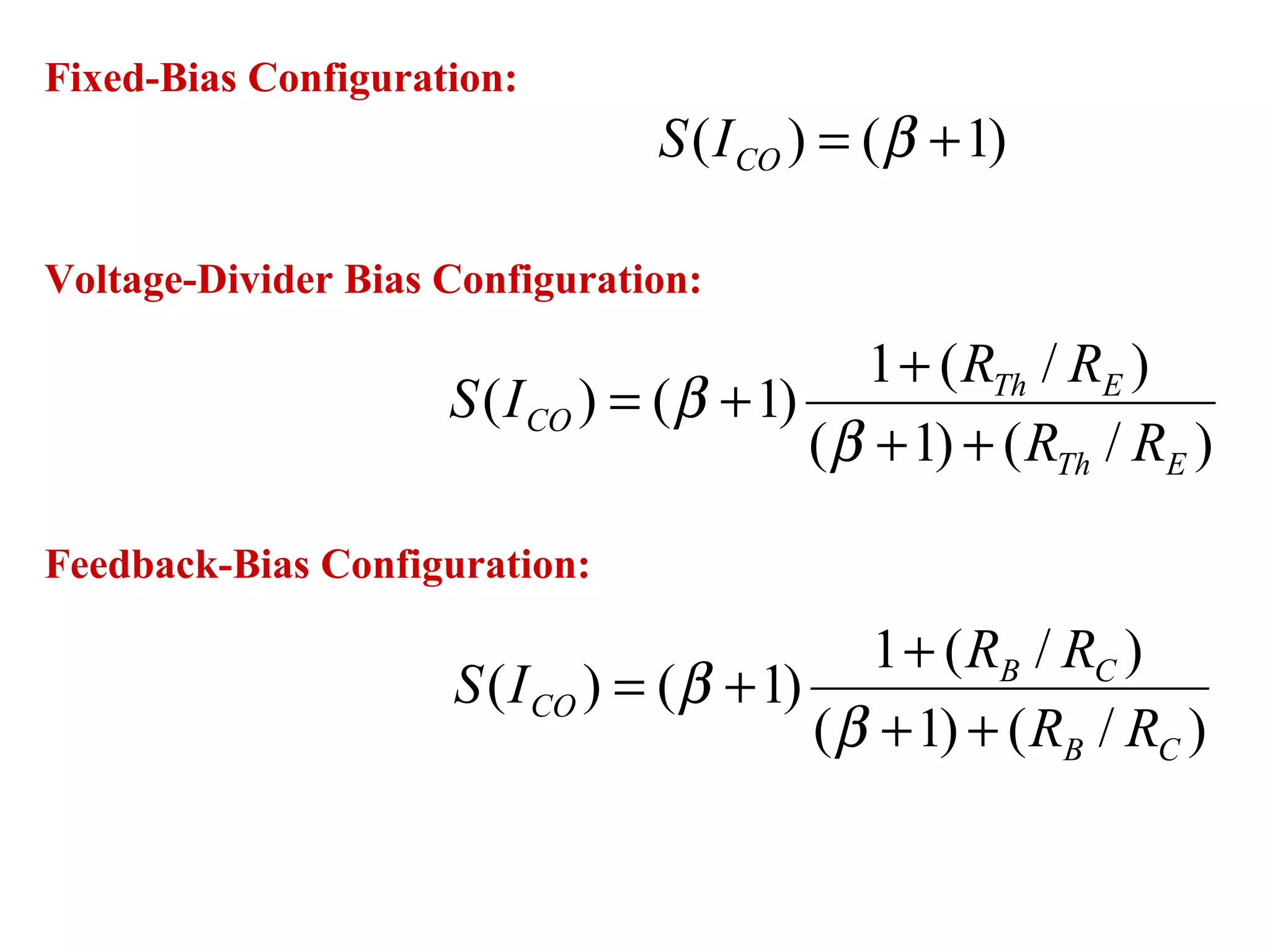
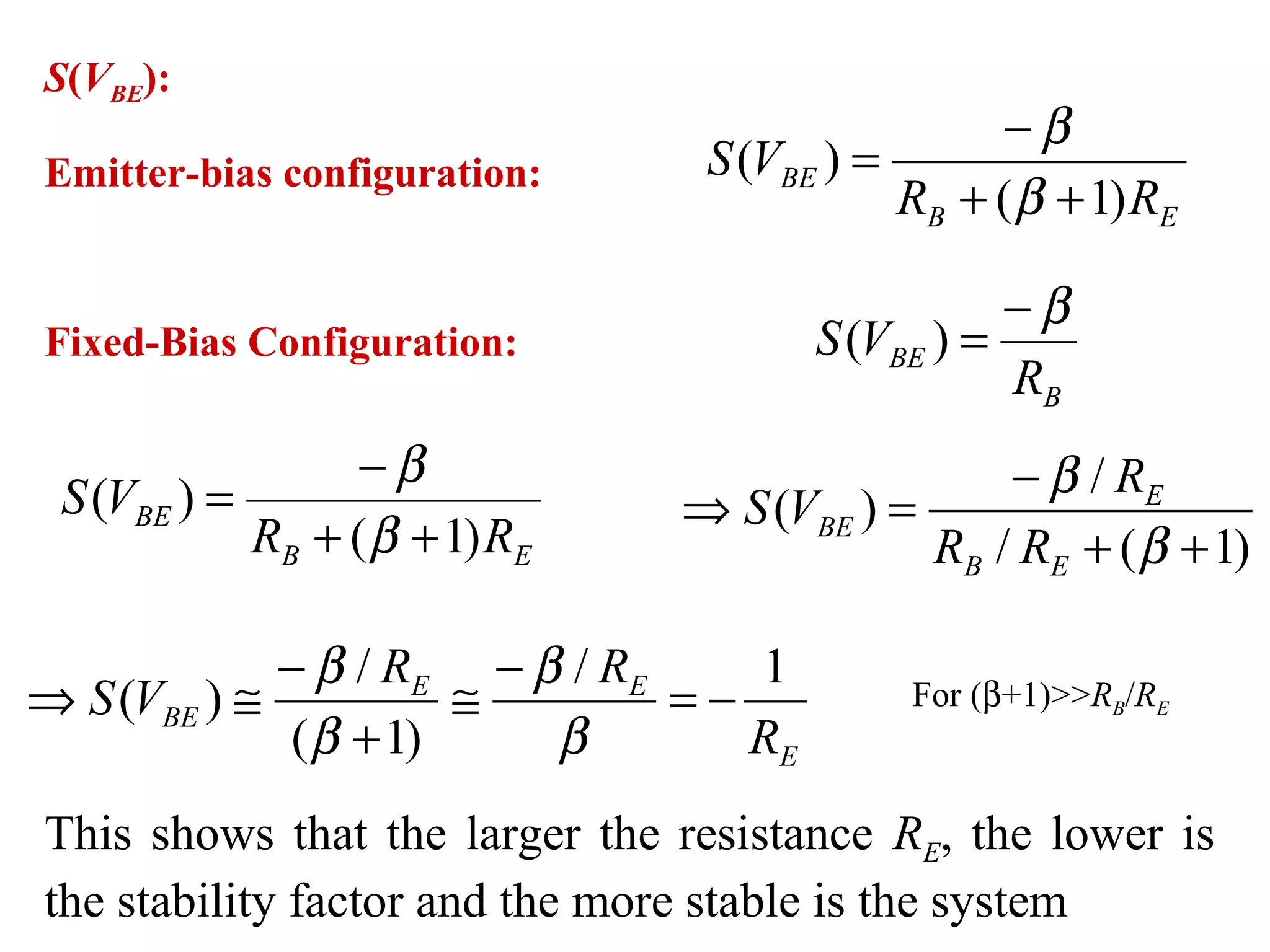
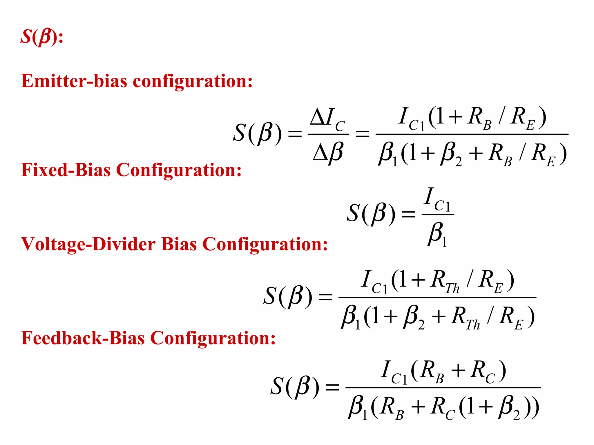
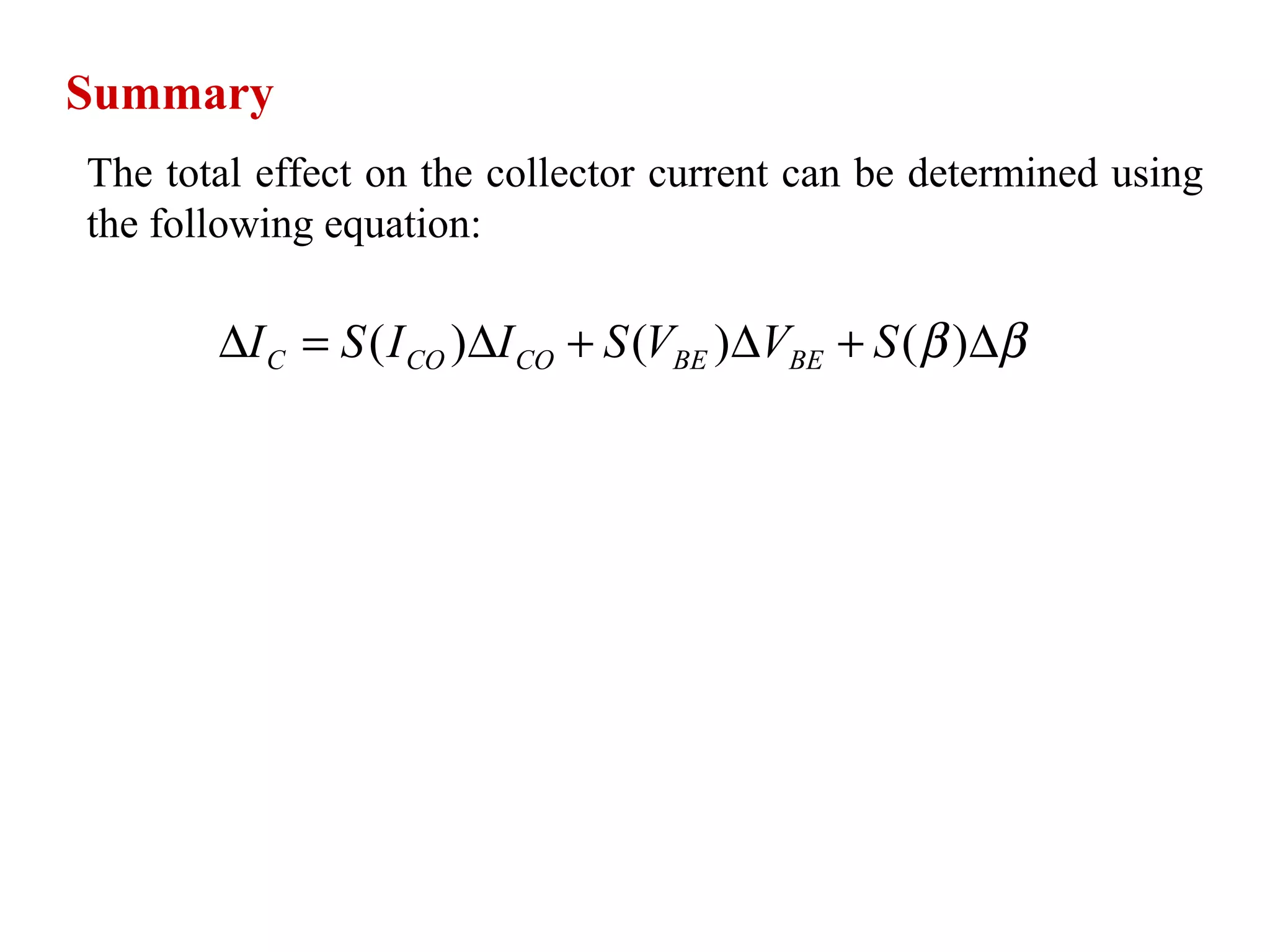
DC biasing applies fixed voltages to transistors to place them in an operating region for amplification. The operating point defines the transistor's quiescent operating conditions under DC. Stability refers to a circuit's insensitivity to parameter variations like temperature. Emitter-stabilized and voltage divider biasing improve stability over fixed biasing by incorporating an emitter or voltage divider resistor. Feedback biasing further increases stability by introducing negative feedback from collector to base.
![Circuit Values Affect the Q-PointCircuit Values Affect the Q-Point
[Movement of the Q-point with increasing level of IB]](https://image.slidesharecdn.com/lecture-4-dcbiasingofbjts-150222163832-conversion-gate01/75/dc-biasing-of-bjt-20-2048.jpg)
![Circuit Values Affect the Q-PointCircuit Values Affect the Q-Point
[Effect of an increasing level of RC on the load line the
Q-point]](https://image.slidesharecdn.com/lecture-4-dcbiasingofbjts-150222163832-conversion-gate01/75/dc-biasing-of-bjt-21-2048.jpg)
![Circuit Values Affect the Q-PointCircuit Values Affect the Q-Point
[Effect of lower values of VCC on the load line the Q-
point]](https://image.slidesharecdn.com/lecture-4-dcbiasingofbjts-150222163832-conversion-gate01/75/dc-biasing-of-bjt-22-2048.jpg)
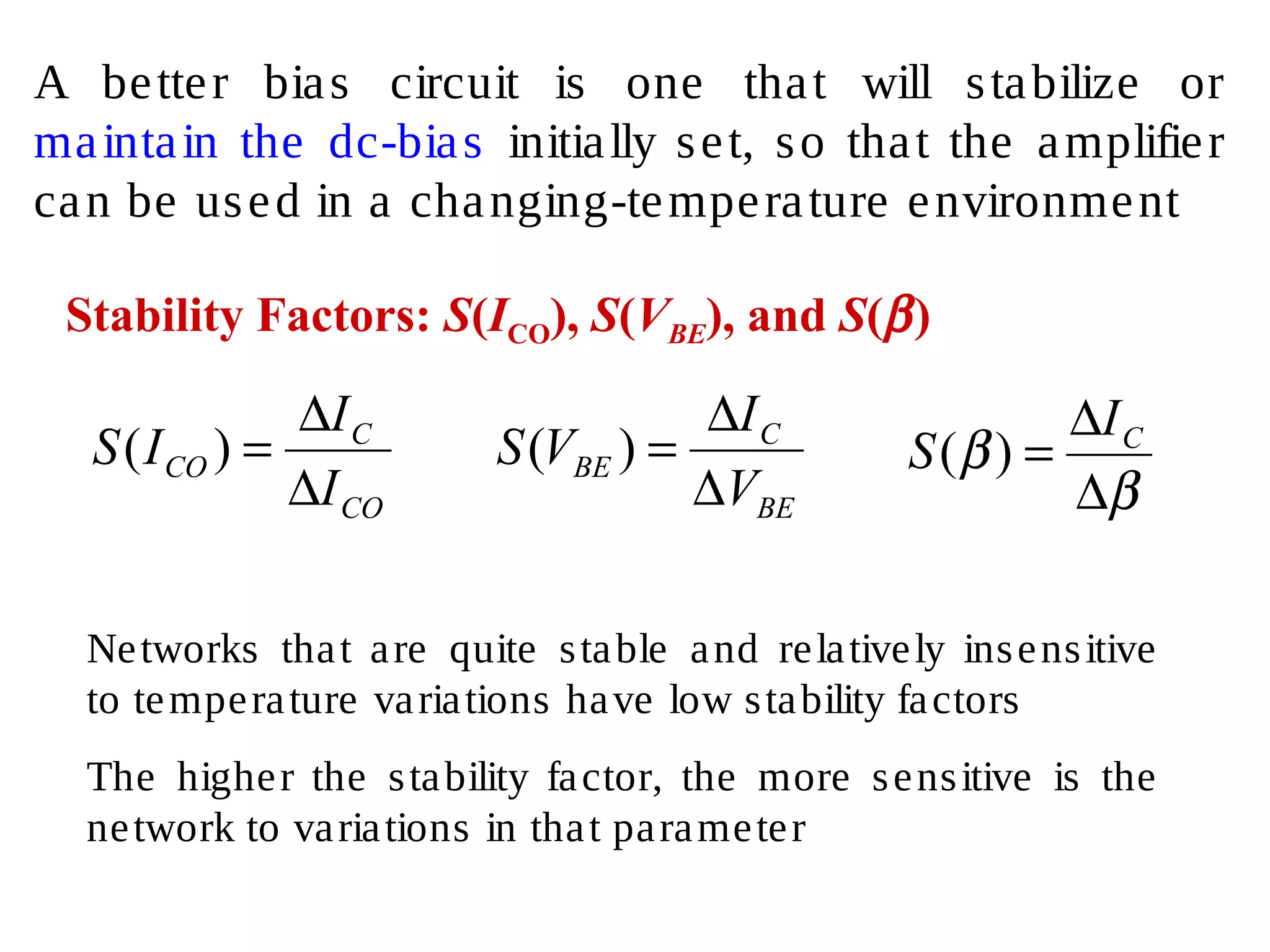
![Improved Biased StabilityImproved Biased Stability
Stability refers to a circuit condition in which the currents
and voltages will remain fairly constant over a wide range
of temperatures and transistor Beta (β) values
Adding RE to the emitter improves the stability of a transistor
β IB(µA) IC(mA) VCE(V)
75 30.24 2.27 9.91
100 28.81 3.63 9.11
[For Emitter Bias Case]
β IB(µA) IC(mA) VCE(V)
75 47.08 3.53 4.23
100 47.08 4.71 1.64
[For Fixed Bias Case]](https://image.slidesharecdn.com/lecture-4-dcbiasingofbjts-150222163832-conversion-gate01/75/dc-biasing-of-bjt-27-2048.jpg)
![[Variation of stability factor with the resistor ratio RB/RE for
the emitter-bias configuration]](https://image.slidesharecdn.com/lecture-4-dcbiasingofbjts-150222163832-conversion-gate01/75/dc-biasing-of-bjt-45-2048.jpg)


![Bipolar Junction Transistor Biasing [Types]](https://cdn.slidesharecdn.com/ss_thumbnails/ele307module2working-1-251030220651-e41b5c93-thumbnail.jpg?width=640&height=640&fit=bounds)


