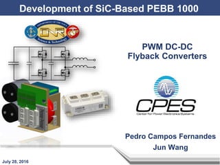
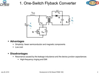
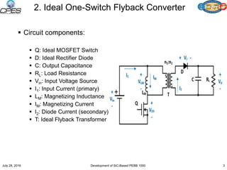
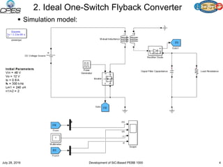
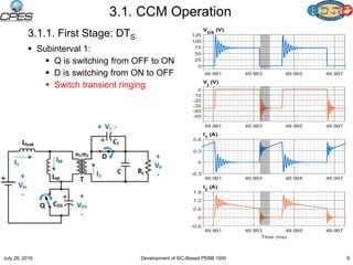
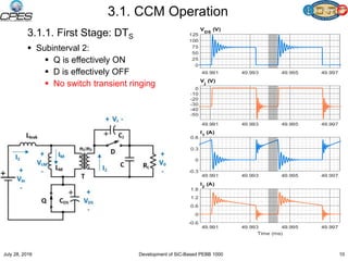
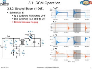
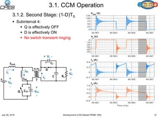
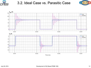
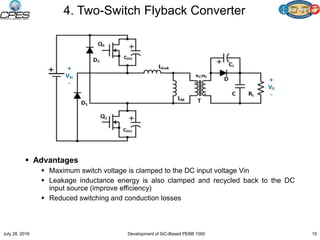
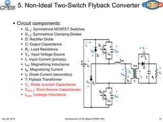
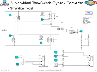
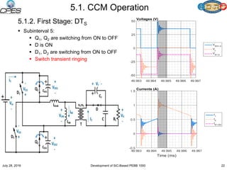
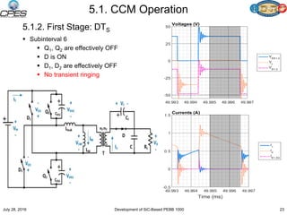
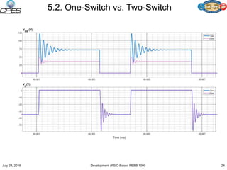
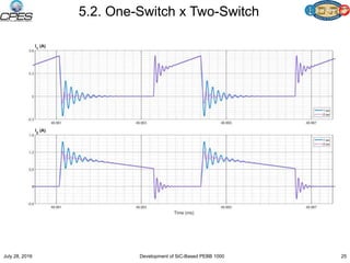
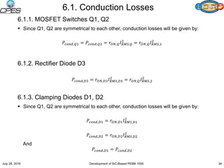
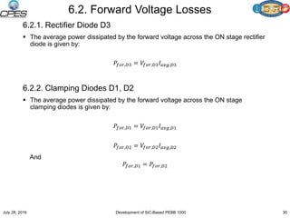
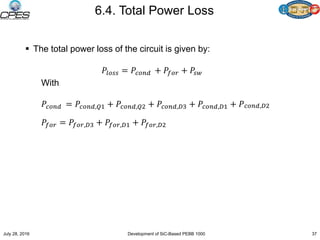
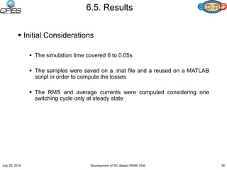
Development of SiC-Based PEBB 1000
July 28, 2016
PWM DC-DC
Flyback Converters
Pedro Campos Fernandes
Jun Wang
1. One-Switch Flyback Converter
 Advantages
 Simplicity: fewer semiconductor and magnetic components
 Low cost
 Disadvantages
 Resonance caused by the leakage inductance and the device junction capacitances
 High-frequency ringing and EMI
July 28, 2016 2Development of SiC-Based PEBB 1000
2. Ideal One-Switch Flyback Converter
 Circuit components:
 Q: Ideal MOSFET Switch
 D: Ideal Rectifier Diode
 C: Output Capacitance
 RL: Load Resistance
 Vin: Input Voltage Source
 I1: Input Current (primary)
 LM: Magnetizing Inductance
 IM: Magnetizing Current
 I2: Diode Current (secondary)
 T: Ideal Flyback Transformer
July 28, 2016 3Development of SiC-Based PEBB 1000
2. Ideal One-Switch Flyback Converter
 Simulation model:
July 28, 2016 4Development of SiC-Based PEBB 1000
2.1. CCM Operation
2.1.1. First Stage: DTS
 Q is ON
 D is OFF
 Energy from the DC source
is stored in LM
July 28, 2016 5Development of SiC-Based PEBB 1000
2.1. CCM Operation
2.1.2. Second Stage: (1-D)TS
 Q is OFF
 D is ON
 Transformer voltage reverses
forward-biasing the rectifier diode
and delivering energy to the output
July 28, 2016 6Development of SiC-Based PEBB 1000
3. Non-Ideal One-Switch Flyback Converter
 Circuit components:
 Q: MOSFET Switch
 D: Rectifier Diode
 C: Output Capacitance
 RL: Load Resistance
 Vin: Input Voltage Source
 I1: Input Current (primary)
 LM: Magnetizing Inductance
 IM: Magnetizing Current
 I2: Diode Current (secondary)
 T: Flyback Transformer
 CJ: Diode Junction Capacitance
 CDS: Drain-Source Capacitance
 Lleak: Leakage Inductance
July 28, 2016 7Development of SiC-Based PEBB 1000
3. Non-Ideal One-Switch Flyback Converter
 Simulation model:
July 28, 2016 8Development of SiC-Based PEBB 1000
3.1. CCM Operation
3.1.1. First Stage: DTS
 Subinterval 1:
 Q is switching from OFF to ON
 D is switching from ON to OFF
 Switch transient ringing
July 28, 2016 9Development of SiC-Based PEBB 1000
3.1. CCM Operation
3.1.1. First Stage: DTS
 Subinterval 2:
 Q is effectively ON
 D is effectively OFF
 No switch transient ringing
July 28, 2016 10Development of SiC-Based PEBB 1000
3.1. CCM Operation
3.1.2. Second Stage: (1-D)TS
 Subinterval 3:
 Q is switching from ON to OFF
 D is switching from OFF to ON
 Switch transient ringing
July 28, 2016 11Development of SiC-Based PEBB 1000
3.1. CCM Operation
3.1.2. Second Stage: (1-D)TS
 Subinterval 4:
 Q is effectively OFF
 D is effectively ON
 No switch transient ringing
July 28, 2016 12Development of SiC-Based PEBB 1000
3.2. Ideal Case vs. Parasitic Case
July 28, 2016 Development of SiC-Based PEBB 1000 13
3.2. Ideal Case vs. Parasitic Case
July 28, 2016 Development of SiC-Based PEBB 1000 14
4. Two-Switch Flyback Converter
 Advantages
 Maximum switch voltage is clamped to the DC input voltage Vin
 Leakage inductance energy is also clamped and recycled back to the DC
input source (improve efficiency)
 Reduced switching and conduction losses
July 28, 2016 Development of SiC-Based PEBB 1000 15
5. Non-Ideal Two-Switch Flyback Converter
 Circuit components:
 Q1,2: Symmetrical MOSFET Switches
 D1,2: Symmetrical Clamping Diodes
 D: Rectifier Diode
 C: Output Capacitance
 RL: Load Resistance
 Vin: Input Voltage Source
 I1: Input Current (primary)
 LM: Magnetizing Inductance
 IM: Magnetizing Current
 I2: Diode Current (secondary)
 T: Flyback Transformer
 CJ: Diode Junction Capacitance
 CDS1,2: Drain-Source Capacitances
 Lleak: Leakage Inductance
July 28, 2016 16Development of SiC-Based PEBB 1000
5. Non-Ideal Two-Switch Flyback Converter
 Simulation model:
July 28, 2016 17Development of SiC-Based PEBB 1000
5.1. CCM Operation
5.1.1. First Stage: DTS
 Subinterval 1:
 Q1, Q2 are switching from OFF to ON
 D is switching from ON to OFF
 D1, D2 are OFF
 Switch transient ringing
July 28, 2016 18Development of SiC-Based PEBB 1000
5.1. CCM Operation
5.1.1. First Stage: DTS
 Subinterval 2:
 Q1, Q2 are effectively ON
 D is effectively OFF
 D1, D2 are OFF
 No transient ringing
July 28, 2016 19Development of SiC-Based PEBB 1000
5.1. CCM Operation
5.1.2. Second Stage: (1-D)TS
 Subinterval 3:
 Q1, Q2 are switching from ON to OFF
 D is switching from OFF to ON
 D1, D2 are OFF
 Voltage spike
July 28, 2016 20Development of SiC-Based PEBB 1000
5.1. CCM Operation
5.1.2. Second Stage: (1-D)TS
 Subinterval 4:
 Q1, Q2 are switching from ON to OFF
 D is effectively ON
 D1, D2 are ON
 Switch voltages VDS1, VDS2 are clamped
to Vin
July 28, 2016 21Development of SiC-Based PEBB 1000
5.1. CCM Operation
5.1.2. First Stage: DTS
 Subinterval 5:
 Q1, Q2 are switching from ON to OFF
 D is ON
 D1, D2 are switching from ON to OFF
 Switch transient ringing
July 28, 2016 22Development of SiC-Based PEBB 1000
5.1. CCM Operation
5.1.2. First Stage: DTS
 Subinterval 6
 Q1, Q2 are effectively OFF
 D is ON
 D1, D2 are effectively OFF
 No transient ringing
July 28, 2016 23Development of SiC-Based PEBB 1000
5.2. One-Switch vs. Two-Switch
July 28, 2016 Development of SiC-Based PEBB 1000 24
5.2. One-Switch x Two-Switch
July 28, 2016 Development of SiC-Based PEBB 1000 25
5.3. Component Mismatches
 Real applications do not provide perfect symmetry
between junction capacitances and gate driver signals
 There are mismatches between these variables and
they lead to different behaviors during the converter
operation
July 28, 2016 Development of SiC-Based PEBB 1000 26
5.3. Component Mismatches
 Two types of mismatch will be covered:
 20% mismatch on drain-source capacitance of the low side
MOSFET switch Q2 given the high side MOSFET switch Q1
as reference
 5% delay (given the period as reference) on the gate driver of
the low side MOSFET switch Q2
July 28, 2016 Development of SiC-Based PEBB 1000 27
5.3. Component Mismatches
5.3.1. Capacitance Mismatch
 CDS1 = 120 pF and CDS2 = 144 pF
 Q1 is clamped earlier than Q2, i.e.,
D1 starts conducting earlier than D2
 Q1, Q2 voltages reach different
steady values after the ringing dies
July 28, 2016 Development of SiC-Based PEBB 1000 28
5.3. Component Mismatches
5.3.2. Gate Drive Delay Mismatch
 DelayQ1 = 0 s and DelayQ2 = 0.17 us
 Q2 turns ON later, so Q1 will be clamped
earlier
 Q1 turns ON earlier, leading to another
clamping action during the delayed turn ON
of Q2
July 28, 2016 Development of SiC-Based PEBB 1000 29
5.3. Component Mismatches
5.3.3. Merged Mismatch
July 28, 2016 Development of SiC-Based PEBB 1000 30
5.3. Component Mismatches
 Possible Solutions
 Design an integrated solution with complete control circuit and
gate drive for both high side (Q1) and low side (Q2) switches
 Work with safety margins so that the circuit can still present
good performance for a certain percentage of mismatch
July 28, 2016 Development of SiC-Based PEBB 1000 31
6. Power Losses on Flyback Converters
 Design considerations:
 Zero winding resistances (rprimary = rsecondary = 0)
 Zero leakage resistance
 The MOSFET switches and clamping diodes are considered
symmetrical to each other
 Two-Switch topology - switches model: IRF510
 100 V, 5 A, ron,max = 0.85 Ω and CDS = 60 pF
 One-Switch topology - switch model: IRF840
 500 V, 8 A, ron,max = 0.54 Ω and CDS = 120 pF
 Rectifier Diode model: MBR10100
 100 V, 10 A, VF = 0.65 V and rF = 20 mΩ with CJ = 200 pF
 Clamping Diodes model: MBR10100
 100 V, 10 A, VF = 0.65 V and rF = 20 mΩ with CJ = 0 F
July 28, 2016 Development of SiC-Based PEBB 1000 32
6. Power Losses on Flyback Converters
 Losses presented by the design:
 Conduction Losses
 Forward Voltage Losses
 Switching Losses
July 28, 2016 Development of SiC-Based PEBB 1000 33
6.1. Conduction Losses
6.1.1. MOSFET Switches Q1, Q2
 Since Q1, Q2 are symmetrical to each other, conduction losses will be given by:
𝑃𝑐𝑜𝑛𝑑,𝑄1 = 𝑃𝑐𝑜𝑛𝑑,𝑄2 = 𝑟𝑂𝑁,𝑄 𝐼 𝑅𝑀𝑆,𝑄
2
= 𝑟𝑂𝑁,𝑄 𝐼 𝑅𝑀𝑆,1
2
6.1.2. Rectifier Diode D3
𝑃𝑐𝑜𝑛𝑑,𝐷3 = 𝑟𝑂𝑁,𝐷3 𝐼 𝑅𝑀𝑆,𝐷3
2
= 𝑟𝑂𝑁,𝑄 𝐼 𝑅𝑀𝑆,2
2
6.1.3. Clamping Diodes D1, D2
 Since Q1, Q2 are symmetrical to each other, conduction losses will be given by:
𝑃𝑐𝑜𝑛𝑑,𝐷1 = 𝑟𝑂𝑁,𝐷1 𝐼 𝑅𝑀𝑆,𝐷1
2
𝑃𝑐𝑜𝑛𝑑,𝐷2 = 𝑟𝑂𝑁,𝐷2 𝐼 𝑅𝑀𝑆,𝐷2
2
And
𝑃𝑐𝑜𝑛𝑑,𝐷1 = 𝑃𝑐𝑜𝑛𝑑,𝐷2
July 28, 2016 Development of SiC-Based PEBB 1000 34
6.2. Forward Voltage Losses
6.2.1. Rectifier Diode D3
 The average power dissipated by the forward voltage across the ON stage rectifier
diode is given by:
𝑃𝑓𝑜𝑟,𝐷3 = 𝑉𝑓𝑜𝑟,𝐷3 𝐼 𝑎𝑣𝑔,𝐷3
6.2.2. Clamping Diodes D1, D2
 The average power dissipated by the forward voltage across the ON stage
clamping diodes is given by:
𝑃𝑓𝑜𝑟,𝐷1 = 𝑉𝑓𝑜𝑟,𝐷1 𝐼 𝑎𝑣𝑔,𝐷1
𝑃𝑓𝑜𝑟,𝐷2 = 𝑉𝑓𝑜𝑟,𝐷2 𝐼 𝑎𝑣𝑔,𝐷2
And
𝑃𝑓𝑜𝑟,𝐷1 = 𝑃𝑓𝑜𝑟,𝐷2
July 28, 2016 Development of SiC-Based PEBB 1000 35
6.3. Switching Losses
 Switching Losses on the MOSFET switches can be obtained by
the simplified formulation presented on [4]:
𝑃𝑠𝑤,𝑄1 =
1
2
𝑓𝑠𝑤 𝐶 𝐷𝑆1 𝑉𝐷𝑆1
2
𝑃𝑠𝑤,𝑄2 =
1
2
𝑓𝑠𝑤 𝐶 𝐷𝑆2 𝑉𝐷𝑆2
2
And
𝑃𝑠𝑤,𝑄1 = 𝑃𝑠𝑤,𝑄2 = 𝑃𝑠𝑤
July 28, 2016 Development of SiC-Based PEBB 1000 36
6.4. Total Power Loss
 The total power loss of the circuit is given by:
𝑃𝑙𝑜𝑠𝑠 = 𝑃𝑐𝑜𝑛𝑑 + 𝑃𝑓𝑜𝑟 + 𝑃𝑠𝑤
With
𝑃𝑐𝑜𝑛𝑑 = 𝑃𝑐𝑜𝑛𝑑,𝑄1 + 𝑃𝑐𝑜𝑛𝑑,𝑄2 + 𝑃𝑐𝑜𝑛𝑑,𝐷3 + 𝑃𝑐𝑜𝑛𝑑,𝐷1 + 𝑃 𝑐𝑜𝑛𝑑,𝐷2
𝑃𝑓𝑜𝑟 = 𝑃𝑓𝑜𝑟,𝐷3 + 𝑃𝑓𝑜𝑟,𝐷1 + 𝑃𝑓𝑜𝑟,𝐷2
July 28, 2016 Development of SiC-Based PEBB 1000 37
6.5. Results
 Initial Considerations
 The simulation time covered 0 to 0.05s
 The samples were saved on a .mat file and a reused on a MATLAB
script in order to compute the losses
 The RMS and average currents were computed considering one
switching cycle only at steady state
July 28, 2016 Development of SiC-Based PEBB 1000 38
6.5. Results
July 28, 2016 Development of SiC-Based PEBB 1000 39
0.064
0.353
0.433
0.849
0.874
0.074
0.355
0.042
0.470
0.924
0
0.1
0.2
0.3
0.4
0.5
0.6
0.7
0.8
0.9
1
Condcution Losses Forward Voltage Losses Switching Losses Total Losses Efficiency
Power Losses at CCM (W)
One-Switch Two-Switch
6.5. Results
 Comparison of the performance of the converters in
CCM:
 The conduction losses slightly increased due to the presence
of more components on the two-switch topology
 The switching losses were drastically reduced
 The efficiency increased 5 %
July 28, 2016 Development of SiC-Based PEBB 1000 40
6.5. Results
July 28, 2016 Development of SiC-Based PEBB 1000 41
0.064
0.353
0.433
0.849
0.874
0.084
0.367
0.140
0.592
0.912
0.074
0.355
0.042
0.470
0.924
0.102
0.365
0.011
0.477
0.927
0
0.1
0.2
0.3
0.4
0.5
0.6
0.7
0.8
0.9
1
Conduction Losses Forward Voltage Losses Switching Losses Total Losses Efficency
Power Losses at CCM and BCM (W)
One-Switch CCM One-Switch BCM Two-Switch CCM Two-Switch BCM
6.5. Results
 Comparison of the performance of the converters in
CCM vs. BCM:
 Higher conduction losses at BCM
 Lower switching losses for both topologies at BCM
 Higher efficiency for both topologies at BCM
July 28, 2016 Development of SiC-Based PEBB 1000 42
7. Conclusion
 Does the Two-Switch Flyback Converter present a
better performance when compared to the One-Switch
topology?
Voltage across the MOSFET switches is clamped to Vin (no
high-voltage spikes)
Lower ringing effect
Lower switching losses
Higher efficiency
July 28, 2016 Development of SiC-Based PEBB 1000 43
8. References
[1] “Improving the Performance of Traditional Flyback-Topology With Two-Switch –Approach”, J.
Pesonen; Texas Instruments
[2] “Understand Two-Switch Forward/Flyback Converters”, Y. Xi, R. Bell; National Semiconductor
[3] “Hard-Switching and Soft-Switching Two-Switch Flyback PWM DC-DC Converters and Winding
Loss due to Harmonics in High-Frequency Transformers”, D. M. Bellur, Wright State University
[4] “Two-Switch Flyback PWM DC-DC Converter in Continuous-Conduction Mode”, D. M. Bellur, M.
K. Kazimierczuk, Wright State University
[5] “Fundamentals of Power Electronics”, R. W. Erickson, D. Maksimovic, University of Colorado
Boulder
[6] “Characterization and Modeling of High-Switching-Speed Behavior of SiC Active Devices”,
Zheng Chen; Virginia Polytechnic Institute and State University
[7] “AN-9010 MOSFET Basics”, Fairchild Semiconductor
[8] “Analysis of SiC MOSFETs under Hard and Soft-Switching”, M. R. Ahmed, R. Todd, A. J.
Forsyth, The University of Manchester, UK
[9] “Power Electronics - A First Course”, N. Mohan, University of Minnesota
[10] “Development of an Isolated Flyback Converter Employing Boundary-Mode Operation and
Magnetic Flux Sensing Feedback”, M. V. Kenia, Massachusetts Institute of Technology
July 28, 2016 Development of SiC-Based PEBB 1000 44

Flyback Converters v4

  • 1.
    Development of SiC-BasedPEBB 1000 July 28, 2016 PWM DC-DC Flyback Converters Pedro Campos Fernandes Jun Wang
  • 2.
    1. One-Switch FlybackConverter  Advantages  Simplicity: fewer semiconductor and magnetic components  Low cost  Disadvantages  Resonance caused by the leakage inductance and the device junction capacitances  High-frequency ringing and EMI July 28, 2016 2Development of SiC-Based PEBB 1000
  • 3.
    2. Ideal One-SwitchFlyback Converter  Circuit components:  Q: Ideal MOSFET Switch  D: Ideal Rectifier Diode  C: Output Capacitance  RL: Load Resistance  Vin: Input Voltage Source  I1: Input Current (primary)  LM: Magnetizing Inductance  IM: Magnetizing Current  I2: Diode Current (secondary)  T: Ideal Flyback Transformer July 28, 2016 3Development of SiC-Based PEBB 1000
  • 4.
    2. Ideal One-SwitchFlyback Converter  Simulation model: July 28, 2016 4Development of SiC-Based PEBB 1000
  • 5.
    2.1. CCM Operation 2.1.1.First Stage: DTS  Q is ON  D is OFF  Energy from the DC source is stored in LM July 28, 2016 5Development of SiC-Based PEBB 1000
  • 6.
    2.1. CCM Operation 2.1.2.Second Stage: (1-D)TS  Q is OFF  D is ON  Transformer voltage reverses forward-biasing the rectifier diode and delivering energy to the output July 28, 2016 6Development of SiC-Based PEBB 1000
  • 7.
    3. Non-Ideal One-SwitchFlyback Converter  Circuit components:  Q: MOSFET Switch  D: Rectifier Diode  C: Output Capacitance  RL: Load Resistance  Vin: Input Voltage Source  I1: Input Current (primary)  LM: Magnetizing Inductance  IM: Magnetizing Current  I2: Diode Current (secondary)  T: Flyback Transformer  CJ: Diode Junction Capacitance  CDS: Drain-Source Capacitance  Lleak: Leakage Inductance July 28, 2016 7Development of SiC-Based PEBB 1000
  • 8.
    3. Non-Ideal One-SwitchFlyback Converter  Simulation model: July 28, 2016 8Development of SiC-Based PEBB 1000
  • 9.
    3.1. CCM Operation 3.1.1.First Stage: DTS  Subinterval 1:  Q is switching from OFF to ON  D is switching from ON to OFF  Switch transient ringing July 28, 2016 9Development of SiC-Based PEBB 1000
  • 10.
    3.1. CCM Operation 3.1.1.First Stage: DTS  Subinterval 2:  Q is effectively ON  D is effectively OFF  No switch transient ringing July 28, 2016 10Development of SiC-Based PEBB 1000
  • 11.
    3.1. CCM Operation 3.1.2.Second Stage: (1-D)TS  Subinterval 3:  Q is switching from ON to OFF  D is switching from OFF to ON  Switch transient ringing July 28, 2016 11Development of SiC-Based PEBB 1000
  • 12.
    3.1. CCM Operation 3.1.2.Second Stage: (1-D)TS  Subinterval 4:  Q is effectively OFF  D is effectively ON  No switch transient ringing July 28, 2016 12Development of SiC-Based PEBB 1000
  • 13.
    3.2. Ideal Casevs. Parasitic Case July 28, 2016 Development of SiC-Based PEBB 1000 13
  • 14.
    3.2. Ideal Casevs. Parasitic Case July 28, 2016 Development of SiC-Based PEBB 1000 14
  • 15.
    4. Two-Switch FlybackConverter  Advantages  Maximum switch voltage is clamped to the DC input voltage Vin  Leakage inductance energy is also clamped and recycled back to the DC input source (improve efficiency)  Reduced switching and conduction losses July 28, 2016 Development of SiC-Based PEBB 1000 15
  • 16.
    5. Non-Ideal Two-SwitchFlyback Converter  Circuit components:  Q1,2: Symmetrical MOSFET Switches  D1,2: Symmetrical Clamping Diodes  D: Rectifier Diode  C: Output Capacitance  RL: Load Resistance  Vin: Input Voltage Source  I1: Input Current (primary)  LM: Magnetizing Inductance  IM: Magnetizing Current  I2: Diode Current (secondary)  T: Flyback Transformer  CJ: Diode Junction Capacitance  CDS1,2: Drain-Source Capacitances  Lleak: Leakage Inductance July 28, 2016 16Development of SiC-Based PEBB 1000
  • 17.
    5. Non-Ideal Two-SwitchFlyback Converter  Simulation model: July 28, 2016 17Development of SiC-Based PEBB 1000
  • 18.
    5.1. CCM Operation 5.1.1.First Stage: DTS  Subinterval 1:  Q1, Q2 are switching from OFF to ON  D is switching from ON to OFF  D1, D2 are OFF  Switch transient ringing July 28, 2016 18Development of SiC-Based PEBB 1000
  • 19.
    5.1. CCM Operation 5.1.1.First Stage: DTS  Subinterval 2:  Q1, Q2 are effectively ON  D is effectively OFF  D1, D2 are OFF  No transient ringing July 28, 2016 19Development of SiC-Based PEBB 1000
  • 20.
    5.1. CCM Operation 5.1.2.Second Stage: (1-D)TS  Subinterval 3:  Q1, Q2 are switching from ON to OFF  D is switching from OFF to ON  D1, D2 are OFF  Voltage spike July 28, 2016 20Development of SiC-Based PEBB 1000
  • 21.
    5.1. CCM Operation 5.1.2.Second Stage: (1-D)TS  Subinterval 4:  Q1, Q2 are switching from ON to OFF  D is effectively ON  D1, D2 are ON  Switch voltages VDS1, VDS2 are clamped to Vin July 28, 2016 21Development of SiC-Based PEBB 1000
  • 22.
    5.1. CCM Operation 5.1.2.First Stage: DTS  Subinterval 5:  Q1, Q2 are switching from ON to OFF  D is ON  D1, D2 are switching from ON to OFF  Switch transient ringing July 28, 2016 22Development of SiC-Based PEBB 1000
  • 23.
    5.1. CCM Operation 5.1.2.First Stage: DTS  Subinterval 6  Q1, Q2 are effectively OFF  D is ON  D1, D2 are effectively OFF  No transient ringing July 28, 2016 23Development of SiC-Based PEBB 1000
  • 24.
    5.2. One-Switch vs.Two-Switch July 28, 2016 Development of SiC-Based PEBB 1000 24
  • 25.
    5.2. One-Switch xTwo-Switch July 28, 2016 Development of SiC-Based PEBB 1000 25
  • 26.
    5.3. Component Mismatches Real applications do not provide perfect symmetry between junction capacitances and gate driver signals  There are mismatches between these variables and they lead to different behaviors during the converter operation July 28, 2016 Development of SiC-Based PEBB 1000 26
  • 27.
    5.3. Component Mismatches Two types of mismatch will be covered:  20% mismatch on drain-source capacitance of the low side MOSFET switch Q2 given the high side MOSFET switch Q1 as reference  5% delay (given the period as reference) on the gate driver of the low side MOSFET switch Q2 July 28, 2016 Development of SiC-Based PEBB 1000 27
  • 28.
    5.3. Component Mismatches 5.3.1.Capacitance Mismatch  CDS1 = 120 pF and CDS2 = 144 pF  Q1 is clamped earlier than Q2, i.e., D1 starts conducting earlier than D2  Q1, Q2 voltages reach different steady values after the ringing dies July 28, 2016 Development of SiC-Based PEBB 1000 28
  • 29.
    5.3. Component Mismatches 5.3.2.Gate Drive Delay Mismatch  DelayQ1 = 0 s and DelayQ2 = 0.17 us  Q2 turns ON later, so Q1 will be clamped earlier  Q1 turns ON earlier, leading to another clamping action during the delayed turn ON of Q2 July 28, 2016 Development of SiC-Based PEBB 1000 29
  • 30.
    5.3. Component Mismatches 5.3.3.Merged Mismatch July 28, 2016 Development of SiC-Based PEBB 1000 30
  • 31.
    5.3. Component Mismatches Possible Solutions  Design an integrated solution with complete control circuit and gate drive for both high side (Q1) and low side (Q2) switches  Work with safety margins so that the circuit can still present good performance for a certain percentage of mismatch July 28, 2016 Development of SiC-Based PEBB 1000 31
  • 32.
    6. Power Losseson Flyback Converters  Design considerations:  Zero winding resistances (rprimary = rsecondary = 0)  Zero leakage resistance  The MOSFET switches and clamping diodes are considered symmetrical to each other  Two-Switch topology - switches model: IRF510  100 V, 5 A, ron,max = 0.85 Ω and CDS = 60 pF  One-Switch topology - switch model: IRF840  500 V, 8 A, ron,max = 0.54 Ω and CDS = 120 pF  Rectifier Diode model: MBR10100  100 V, 10 A, VF = 0.65 V and rF = 20 mΩ with CJ = 200 pF  Clamping Diodes model: MBR10100  100 V, 10 A, VF = 0.65 V and rF = 20 mΩ with CJ = 0 F July 28, 2016 Development of SiC-Based PEBB 1000 32
  • 33.
    6. Power Losseson Flyback Converters  Losses presented by the design:  Conduction Losses  Forward Voltage Losses  Switching Losses July 28, 2016 Development of SiC-Based PEBB 1000 33
  • 34.
    6.1. Conduction Losses 6.1.1.MOSFET Switches Q1, Q2  Since Q1, Q2 are symmetrical to each other, conduction losses will be given by: 𝑃𝑐𝑜𝑛𝑑,𝑄1 = 𝑃𝑐𝑜𝑛𝑑,𝑄2 = 𝑟𝑂𝑁,𝑄 𝐼 𝑅𝑀𝑆,𝑄 2 = 𝑟𝑂𝑁,𝑄 𝐼 𝑅𝑀𝑆,1 2 6.1.2. Rectifier Diode D3 𝑃𝑐𝑜𝑛𝑑,𝐷3 = 𝑟𝑂𝑁,𝐷3 𝐼 𝑅𝑀𝑆,𝐷3 2 = 𝑟𝑂𝑁,𝑄 𝐼 𝑅𝑀𝑆,2 2 6.1.3. Clamping Diodes D1, D2  Since Q1, Q2 are symmetrical to each other, conduction losses will be given by: 𝑃𝑐𝑜𝑛𝑑,𝐷1 = 𝑟𝑂𝑁,𝐷1 𝐼 𝑅𝑀𝑆,𝐷1 2 𝑃𝑐𝑜𝑛𝑑,𝐷2 = 𝑟𝑂𝑁,𝐷2 𝐼 𝑅𝑀𝑆,𝐷2 2 And 𝑃𝑐𝑜𝑛𝑑,𝐷1 = 𝑃𝑐𝑜𝑛𝑑,𝐷2 July 28, 2016 Development of SiC-Based PEBB 1000 34
  • 35.
    6.2. Forward VoltageLosses 6.2.1. Rectifier Diode D3  The average power dissipated by the forward voltage across the ON stage rectifier diode is given by: 𝑃𝑓𝑜𝑟,𝐷3 = 𝑉𝑓𝑜𝑟,𝐷3 𝐼 𝑎𝑣𝑔,𝐷3 6.2.2. Clamping Diodes D1, D2  The average power dissipated by the forward voltage across the ON stage clamping diodes is given by: 𝑃𝑓𝑜𝑟,𝐷1 = 𝑉𝑓𝑜𝑟,𝐷1 𝐼 𝑎𝑣𝑔,𝐷1 𝑃𝑓𝑜𝑟,𝐷2 = 𝑉𝑓𝑜𝑟,𝐷2 𝐼 𝑎𝑣𝑔,𝐷2 And 𝑃𝑓𝑜𝑟,𝐷1 = 𝑃𝑓𝑜𝑟,𝐷2 July 28, 2016 Development of SiC-Based PEBB 1000 35
  • 36.
    6.3. Switching Losses Switching Losses on the MOSFET switches can be obtained by the simplified formulation presented on [4]: 𝑃𝑠𝑤,𝑄1 = 1 2 𝑓𝑠𝑤 𝐶 𝐷𝑆1 𝑉𝐷𝑆1 2 𝑃𝑠𝑤,𝑄2 = 1 2 𝑓𝑠𝑤 𝐶 𝐷𝑆2 𝑉𝐷𝑆2 2 And 𝑃𝑠𝑤,𝑄1 = 𝑃𝑠𝑤,𝑄2 = 𝑃𝑠𝑤 July 28, 2016 Development of SiC-Based PEBB 1000 36
  • 37.
    6.4. Total PowerLoss  The total power loss of the circuit is given by: 𝑃𝑙𝑜𝑠𝑠 = 𝑃𝑐𝑜𝑛𝑑 + 𝑃𝑓𝑜𝑟 + 𝑃𝑠𝑤 With 𝑃𝑐𝑜𝑛𝑑 = 𝑃𝑐𝑜𝑛𝑑,𝑄1 + 𝑃𝑐𝑜𝑛𝑑,𝑄2 + 𝑃𝑐𝑜𝑛𝑑,𝐷3 + 𝑃𝑐𝑜𝑛𝑑,𝐷1 + 𝑃 𝑐𝑜𝑛𝑑,𝐷2 𝑃𝑓𝑜𝑟 = 𝑃𝑓𝑜𝑟,𝐷3 + 𝑃𝑓𝑜𝑟,𝐷1 + 𝑃𝑓𝑜𝑟,𝐷2 July 28, 2016 Development of SiC-Based PEBB 1000 37
  • 38.
    6.5. Results  InitialConsiderations  The simulation time covered 0 to 0.05s  The samples were saved on a .mat file and a reused on a MATLAB script in order to compute the losses  The RMS and average currents were computed considering one switching cycle only at steady state July 28, 2016 Development of SiC-Based PEBB 1000 38
  • 39.
    6.5. Results July 28,2016 Development of SiC-Based PEBB 1000 39 0.064 0.353 0.433 0.849 0.874 0.074 0.355 0.042 0.470 0.924 0 0.1 0.2 0.3 0.4 0.5 0.6 0.7 0.8 0.9 1 Condcution Losses Forward Voltage Losses Switching Losses Total Losses Efficiency Power Losses at CCM (W) One-Switch Two-Switch
  • 40.
    6.5. Results  Comparisonof the performance of the converters in CCM:  The conduction losses slightly increased due to the presence of more components on the two-switch topology  The switching losses were drastically reduced  The efficiency increased 5 % July 28, 2016 Development of SiC-Based PEBB 1000 40
  • 41.
    6.5. Results July 28,2016 Development of SiC-Based PEBB 1000 41 0.064 0.353 0.433 0.849 0.874 0.084 0.367 0.140 0.592 0.912 0.074 0.355 0.042 0.470 0.924 0.102 0.365 0.011 0.477 0.927 0 0.1 0.2 0.3 0.4 0.5 0.6 0.7 0.8 0.9 1 Conduction Losses Forward Voltage Losses Switching Losses Total Losses Efficency Power Losses at CCM and BCM (W) One-Switch CCM One-Switch BCM Two-Switch CCM Two-Switch BCM
  • 42.
    6.5. Results  Comparisonof the performance of the converters in CCM vs. BCM:  Higher conduction losses at BCM  Lower switching losses for both topologies at BCM  Higher efficiency for both topologies at BCM July 28, 2016 Development of SiC-Based PEBB 1000 42
  • 43.
    7. Conclusion  Doesthe Two-Switch Flyback Converter present a better performance when compared to the One-Switch topology? Voltage across the MOSFET switches is clamped to Vin (no high-voltage spikes) Lower ringing effect Lower switching losses Higher efficiency July 28, 2016 Development of SiC-Based PEBB 1000 43
  • 44.
    8. References [1] “Improvingthe Performance of Traditional Flyback-Topology With Two-Switch –Approach”, J. Pesonen; Texas Instruments [2] “Understand Two-Switch Forward/Flyback Converters”, Y. Xi, R. Bell; National Semiconductor [3] “Hard-Switching and Soft-Switching Two-Switch Flyback PWM DC-DC Converters and Winding Loss due to Harmonics in High-Frequency Transformers”, D. M. Bellur, Wright State University [4] “Two-Switch Flyback PWM DC-DC Converter in Continuous-Conduction Mode”, D. M. Bellur, M. K. Kazimierczuk, Wright State University [5] “Fundamentals of Power Electronics”, R. W. Erickson, D. Maksimovic, University of Colorado Boulder [6] “Characterization and Modeling of High-Switching-Speed Behavior of SiC Active Devices”, Zheng Chen; Virginia Polytechnic Institute and State University [7] “AN-9010 MOSFET Basics”, Fairchild Semiconductor [8] “Analysis of SiC MOSFETs under Hard and Soft-Switching”, M. R. Ahmed, R. Todd, A. J. Forsyth, The University of Manchester, UK [9] “Power Electronics - A First Course”, N. Mohan, University of Minnesota [10] “Development of an Isolated Flyback Converter Employing Boundary-Mode Operation and Magnetic Flux Sensing Feedback”, M. V. Kenia, Massachusetts Institute of Technology July 28, 2016 Development of SiC-Based PEBB 1000 44