More Related Content
Similar to Lect2 up060 (100324)
Similar to Lect2 up060 (100324) (20)
Lect2 up060 (100324)
- 1. Lecture 060 – Capacitors (3/24/10) Page 060-1
LECTURE 060 - CAPACITORS
LECTURE ORGANIZATION
Outline
• Introduction
• pn junction capacitors
• MOSFET gate capacitors
• Conductor-insulator-conductor capacitors
• Deviation from ideal behavior in capacitors
• Summary
CMOS Analog Circuit Design, 2nd Edition Reference
Pages 43-47, 58-59 and 63-64
CMOS Analog Circuit Design © P.E. Allen - 2010
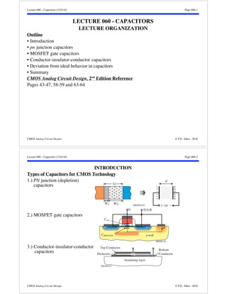
Lecture 060 – Capacitors (3/24/10) Page 060-2
INTRODUCTION
Types of Capacitors for CMOS Technology
1.) PN junction (depletion)
capacitors
2.) MOSFET gate capacitors
3.) Conductor-insulator-conductor
capacitors
d
−− ++− +
−− ++− +
060204-01 + vD −
xd
W1 W2
p+
060207-01
G D,S,B
Cox
n+ n+
p-well
Cjunction
Top Conductor
Bottom
Dielectric Conductor
Insulating layer
060206-02
CMOS Analog Circuit Design © P.E. Allen - 2010
- 2. Lecture 060 – Capacitors (3/24/10) Page 060-3
Characterization of Capacitors
What characterizes a capacitor?
1.) Dissipation (quality factor) of a capacitor is
Q = CRp =
C
Rs
where Rp is the equivalent resistance in parallel with the capacitor, C, and Rs is the
electrical series resistance (ESR) of the capacitor, C.
2.) Parasitic capacitors to ground from each node of the capacitor.
3.) The density of the capacitor in Farads/area.
4.) The absolute and relative accuracies of the capacitor.
5.) The Cmax/Cmin ratio which is the largest value of capacitance to the smallest when
the capacitor is used as a variable capacitor (varactor).
6.) The variation of a variable capacitance with the control voltage.
7.) Linearity, q = Cv.
CMOS Analog Circuit Design © P.E. Allen - 2010
Lecture 060 – Capacitors (3/24/10) Page 060-4
PN JUNCTION CAPACITORS
PN Junction Capacitors in a Well
Generally made by diffusion into the well.
Anode
Cj Cj
p+
n+ n+
Cw
Rwj Rwj Rw
n-well
Substrate
p+
C
rD
VA VB
Anode Cathode
Rwj
Fig. 2.5-011
Depletion
Region
Cathode
p- substrate
Rs
Layout:
Minimize the distance between the p+ and n+ diffusions.
Two different versions have been tested.
n+ diffusion
p+ dif-fusion
1.) Large islands – 9μm on a side
2.) Small islands – 1.2μm on a side n-well
Fig. 2.5-1A
CMOS Analog Circuit Design © P.E. Allen - 2010
- 3. Lecture 060 – Capacitors (3/24/10) Page 060-5
PN-Junction Capacitors – Continued
The anode should be the floating node and the cathode must be connected to ac ground.
Experimental data (Q at 2GHz, 0.5μm CMOS)†:
Qmin Qmax
C
Anode Cathode
R-X
Bridge
Cathode
Voltage
Large Islands
Small Islands
0 0.5 1 1.5 2 2.5 3 3.5
060206-03
4
3.5
3
2.5
2
1.5
1
0.5
0
Large Islands
Cmax Cmin
Small Islands
C
Anode Cathode
R-X
Bridge
Cathode
Voltage
0 0.5 1 1.5 2 2.5 3 3.5
CAnode (pF)
Cathode Voltage (V)
120
100
80
60
40
20
0
QAnode
Cathode Voltage (V)
Terminal Small Islands (598 1.2μm x1.2μm) Large Islands (42 9μm x 9μm)
Under Test Cmax/Cmin Qmin Qmax Cmax/Cmin Qmin Qmax
Anode 1.23 94.5 109 1.32 19 22.6
Cathode 1.21 8.4 9.2 1.29 8.6 9.5
Electrons as majority carriers lead to higher Q because of their higher mobility.
The resistance, Rwj, is reduced in small islands compared with large islands higher Q
† E. Pedersen, “RF CMOS Varactors for 2GHz Applications,” Analog Integrated Circuits and Signal Processing, vol. 26, pp. 27-36, Jan. 2001.
CMOS Analog Circuit Design © P.E. Allen - 2010
Lecture 060 – Capacitors (3/24/10) Page 060-6
MOSFET GATE CAPACITORS
MOSFET Gate Capacitor Structure
The MOSFET gate capacitors have the gate as one terminal of the capacitor and some
combination of the source, drain, and bulk as the other terminal.
In the model of the MOSFET gate capacitor shown below, the gate capacitance is really
two capacitors in series depending on the condition of the channel.
Cgate =
1
1
Cox+
1
Cj
060207-02
Cox
S B
n+ n+
p-well
p+
G D
Cjunction
G
Cox
Channel Resistance
S D
B
Cjunction
Bulk Resistance
CMOS Analog Circuit Design © P.E. Allen - 2010
- 4. Lecture 060 – Capacitors (3/24/10) Page 060-7
MOSFET Gate Capacitor as a function of VGS with D=S=B
Cox Cox
Strong
Inversion
VG-VD,S,B
Operation:
In this configuration, the MOSFET gate capacitor has 5 regions of operation as VGS is
varied. They are:
060207-03
G D,S,B
Cox
n+ n+
p-well
p+
Cjunction
Capacitance
Accumulation
Weak
Inv.
Moderate
Inversion
Depletion
1.) Accumulation
2.) Depletion
3.) Weak inversion
4.) Moderate inversion
5.) Strong inversion
For the first four regions, the gate capacitance is the series combination of Cox and Cj
given as,
Cgate =
1
1
Cox+
1
Cj
CMOS Analog Circuit Design © P.E. Allen - 2010
Lecture 060 – Capacitors (3/24/10) Page 060-8
Use of a 3 Segment Model to Explain the Gate Capacitor Variation
Region Channel R Cox and Cj Cgate 3-Segment Model
Accumulation Large In series and
Cj Cox
Cgate Cox
Depletion Large In series and
Cj Cox
Cgate 0.5Cox
0.5Cj
Weak
Inversion
Large In series and
Cj Cox
Cgate Cj
Moderate
Inversion
Moderate In series and
Cj Cox
Cj Cgate Cox
Strong
Inversion
Small In parallel and
Cj Cox
Cgate Cox
CMOS Analog Circuit Design © P.E. Allen - 2010
- 5. Lecture 060 – Capacitors (3/24/10) Page 060-9
MOSFET Gate Capacitor as a function of VGS with Bulk Fixed (Inversion Mode)
B Capacitance
Cox Cox
VT shift
if VBS ≠ 0
VG-VD,S
060207-04
G D,S
Cox
n+ n+
p-well
p+
Cjunction
Inversion
Mode MOS
0
B=D= S
Conditions:
• D = S, B = VSS
• Accumulation region removed by connecting bulk to VDD
• Nonlinear
• Channel resistance:
Ron =
L
12KP'(VBG-|VT|)
• LDD transistors will give lower Q because of the increased series resistance
CMOS Analog Circuit Design © P.E. Allen - 2010
Lecture 060 – Capacitors (3/24/10) Page 060-10
Inversion Mode NMOS Capacitor
Best results are obtained
when the drain-source are
connected to ac ground.
Experimental Results (Q at
2GHz, 0.5μm CMOS)†:
4.5
4
3.5
3
2.5
2
1.5
Shown in inversion mode
Bulk
p+
Cmax Cmin
VG = 2.1V
n+ n+
Rsj Cj
Cov Cov B
p- substrate/bulk
RX
Meter
VG VD,S
VG = 1.8V
VG = 1.5V
0 0.5 1 1.5 2 2.5 3 3.5
CGate (pF)
Drain/Source Voltage (V)
G D,S
Cox
Rd Cd Csi Cd Rd
Rsi
38
36
34
32
30
28
26
24
22
n- LDD
Qmax Qmin
RX
Meter
VG VD,S
VG = 1.8V
VG = 2.1V
VG = 1.5V
Fig. 2.5-2
0 0.5 1 1.5 2 2.5 3 3.5
Drain/Source Voltage (V) 070617-06
QGate
VG =1.8V: Cmax/Cmin ratio = 2.15 (1.91), Qmax = 34.3 (5.4), and Qmin = 25.8(4.9)
† E. Pedersen, “RF CMOS Varactors for 2GHz Applications,” Analog Integrated Circuits and Signal Processing, vol. 26, pp. 27-36, Jan. 2001.
D,S
G
CMOS Analog Circuit Design © P.E. Allen - 2010
- 6. Lecture 060 – Capacitors (3/24/10) Page 060-11
Accumulation Mode NMOS Gate Capacitor
G B
Cox
n+ n+
Cox
Inversion Accumulation
VG-VD,S,B
060207-05
Capacitance
Depletion
Conditions:
• Remove p+ drain and source and put n+ bulk contacts instead.
• Implements a variable capacitor with a larger transition region between the maximum
and minimum values.
• Reasonably linear capacitor for values of VGB 0
CMOS Analog Circuit Design © P.E. Allen - 2010
Lecture 060 – Capacitors (3/24/10) Page 060-12
Accumulation Mode Capacitor – Continued
Best results are
obtained when the
drain-source are on
ac ground.
G D,S
Shown in depletion mode.
Cox
Bulk
p+
Cw
Rs
Rw
Experimental
Results (Q at 2GHz, 0.5μm CMOS)†:
4
3.6
3.2
2.8
2.4
2
Cmax Cmin
VG = 0.9V
Cov Cov B
n+ n+
VG VD,S
VG = 0.6V
VG = 0.3V
Rd C Rd d Cd
n- well
p- substrate/bulk
n- LDD
RX VG = 0.3V
Meter
0 0.5 1 1.5 2 2.5 3 3.5
CGate (pF)
Drain/Source Voltage (V)
45
40
QGate
35
30
25
Qmax Qmin
VG = 0.9V
VG VD,S
VG = 0.6V
RX
Meter
Fig. 2.5-5
0 0.5 1 1.5 2 2.5 3 3.5
Drain/Source Voltage (V)
070617-07
VG = 0.6V: Cmax/Cmin ratio = 1.69 (1.61), Qmax = 38.3 (15.0), and Qmin = 33.2(13.6)
† E. Pedersen, “RF CMOS Varactors for 2GHz Applications,” Analog Integrated Circuits and Signal Processing, vol. 26, pp. 27-36, Jan. 2001.
D,S
G
CMOS Analog Circuit Design © P.E. Allen - 2010
- 7. Lecture 060 – Capacitors (3/24/10) Page 060-13
CONDUCTOR-INSULATOR-CONDUCTOR CAPACITORS
Polysilicon-Oxide-Polysilicon (Poly-Poly) Capacitors
LOCOS Technology:
A very linear capacitor
with minimum bottom
plate parasitic.
DSM Technology:
A very linear capacitor with
small bottom plate parasitic.
CMOS Analog Circuit Design © P.E. Allen - 2010
Lecture 060 – Capacitors (3/24/10) Page 060-14
Metal-Insulator-Metal (MiM) Capacitors
In some processes, there is a thin dielectric between a metal layer and a special metal
layer called “capacitor top metal”. Typically the capacitance is around 1fF/μm2 and is
at the level below top metal.
Top
Metal
Second level
Protective Insulator Layer
Metal Via
Vias connecting top
plate to top metal
Capacitor Top Metal
Capacitor
dielectric
Inter- from top metal
mediate
Oxide
Layers
Third level
from top metal
Fourth level
from top metal
060530-01
Capacitor bottom plate
Vias connecting bottom
plate to lower metal
Vias connecting bottom
plate to lower metal
Good matching is possible with low parasitics.
CMOS Analog Circuit Design © P.E. Allen - 2010
- 8. Lecture 060 – Capacitors (3/24/10) Page 060-15
Metal-Insulator-Metal Capacitors – Lateral and Vertical Flux
Capacitance between conductors on the same level and use lateral flux.
Fringing field
Metal
Metal
Metal 3 + - + -
- + - +
+ - + -
Fig2.5-9
Metal 2
Metal 1
Top view:
Side view:
These capacitors are sometimes called fractal capacitors because the fractal patterns are
structures that enclose a finite area with a near-infinite perimeter.
The capacitor/area can be increased by a factor of 10 over vertical flux capacitors.
CMOS Analog Circuit Design © P.E. Allen - 2010
Lecture 060 – Capacitors (3/24/10) Page 060-16
More Detail on Horizontal Metal Capacitors†
Some of the possible metal capacitor structures include:
1.) Horizontal parallel plate (HPP).
2.) Parallel wires (PW):
030909-01
Lateral View 030909-02 Top View
† R. Aparicio and A. Hajimiri, “Capacity Limits and Matching Properties of Integrated Capacitors, IEEE J. of Solid-State Circuits, vol. 37, no. 3, March
2002, pp. 384-393.
CMOS Analog Circuit Design © P.E. Allen - 2010
- 9. Lecture 060 – Capacitors (3/24/10) Page 060-17
Horizontal Metal Capacitors - Continued
3.) Vertical parallel plates (VPP):
Vias
030909-03
4.) Vertical bars (VB):
Vias
030909-04
Lateral View Top View
CMOS Analog Circuit Design © P.E. Allen - 2010
Lecture 060 – Capacitors (3/24/10) Page 060-18
Horizontal Metal Capacitors - Continued
Experimental results for a CMOS process with 3 layers of metal, Lmin =0.5μm, tox =
0.95μm and tmetal = 0.63μm for the bottom 2 layers of metal.
Structure Cap. Density
(aF/μm2)
Caver.
(pF)
Std. Dev.
(fF)
Caver.
fres.
(GHz)
Q @
1 GHz
Rs () Break-down
(V)
VPP 158.3 18.99 103 0.0054 3.65 14.5 0.57 355
PW 101.5 33.5 315 0.0094 1.1 8.6 0.55 380
HPP 35.8 6.94 427 0.0615 6.0 21 1.1 690
Experimental results for a digital CMOS process with 7 layers of metal, Lmin =0.24μm,
tox = 0.7μm and tmetal = 0.53μm for the bottom 5 layers of metal. All capacitors = 1pF.
Structure
(1 pF)
Cap. Density
(aF/μm2)
Caver.
(pF)
Area
(μm2)
Cap.
Enhanc
ement
Std.
Dev.
(fF)
Caver.
fres.
(GHz)
Q @
1 GHz
Break-down
(V)
VPP 1512.2 1.01 670 7.4 5.06 0.0050 40 83.2 128
VB 1281.3 1.07 839.7 6.3 14.19 0.0132 37.1 48.7 124
HPP 203.6 1.09 5378 1.0 26.11 0.0239 21 63.8 500
MIM 1100 1.05 960.9 5.4 - - 11 95 -
CMOS Analog Circuit Design © P.E. Allen - 2010
- 10. Lecture 060 – Capacitors (3/24/10) Page 060-19
Horizontal Metal Capacitors - Continued
Histogram of the capacitance distribution for
the above case (1 pF):
Experimental results for a digital CMOS
process with 7 layers of metal, Lmin =
0.24μm, tox = 0.7μm and tmetal = 0.53μm for
the bottom 5 layers of metal (all capacitors =
10pF):
Structure
Cap. Density
Caver.
Area
(10 pF)
(aF/μm2)
(pF)
(μm2)
Number of dice
Cap.
Enhanc
ement
12
10
8
6
4
2
0
HPP
VPP
PW
94 96 98 100 102 104 106
Std.
Dev.
(fF)
Caver.
σc
Caver
fres.
(GHz)
Q @
1 GHz
030909-05
Break-down
(V)
VPP 1480.0 11.46 7749 8.0 73.43 0.0064 11.3 26.6 125
VB 1223.2 10.60 8666 6.6 73.21 0.0069 11.1 17.8 121
HPP 183.6 10.21 55615 1.0 182.1 0.0178 6.17 23.5 495
MIM 1100 10.13 9216 6.0 - - 4.05 25.6 -
CMOS Analog Circuit Design © P.E. Allen - 2010
Lecture 060 – Capacitors (3/24/10) Page 060-20
DEVIATION FROM IDEAL BEHAVIOR IN CAPACITORS
Capacitor Errors
1.) Dielectric gradients
2.) Edge effects
3.) Process biases
4.) Parasitics
5.) Voltage dependence
6.) Temperature dependence
CMOS Analog Circuit Design © P.E. Allen - 2010
- 11. Lecture 060 – Capacitors (3/24/10) Page 060-21
Capacitor Errors - Oxide Gradients
Error due to a variation in dielectric thickness across the wafer.
Common centroid layout - only good for one-dimensional errors:
060207-07
No common centroid layout Common centroid layout
2C C 2C C
An alternate approach is to layout numerous repetitions and connect them randomly to
achieve a statistical error balanced over the entire area of interest.
Improved matching of three components, A, B, and C:
A B C A B C A B C
C A B C A B C A B
B C A B C A B C A
B
A
C 070625-01
CMOS Analog Circuit Design © P.E. Allen - 2010
Lecture 060 – Capacitors (3/24/10) Page 060-22
Capacitor Errors - Edge Effects
There will always be a randomness on the definition of the edge.
However, etching can be influenced by the presence of adjacent structures.
For example,
Matching of A and B are disturbed by the presence of C.
A
C
B
Improved matching achieve by matching the surroundings of A and B.
A B
C
CMOS Analog Circuit Design © P.E. Allen - 2010
- 12. Lecture 060 – Capacitors (3/24/10) Page 060-23
Process Bias on Capacitors
Consider the following two capacitors:
If L1 = L2 = 2μm, W2 = 2W1 = 4μm and
x = 0.1μm, the ratio of C2 to C1 can
be written as,
C2
C1
=
(2-.2)(4-.2)
(2-.2)(2-.2) =
L1
Δx Δx
Δx Δx
C1 L2 C2
W1
3.8
1.8 = 2.11 5.6% error in matching
How can this matching error be reduced?
The capacitor ratios in general can be expressed as,
C2
C1
=
(L2-2x)(W2-2x)
(L1-2x)(W1-2x) =
W2
W1
1-
2x
W2
1-
2x
W1
W2
W1
2x
W2
1-
2x
W1
1+
W2
W2
W1
041022-03
2x
W2
2x
W1
1-
+
Therefore, if W2 = W1, the matching error should be minimized. The best matching
results between two components are achieved when their geometries are identical.
CMOS Analog Circuit Design © P.E. Allen - 2010
Lecture 060 – Capacitors (3/24/10) Page 060-24
Replication Principle
Based on the previous result, a way to minimize the matching error between two or more
geometries is to insure that the matched components have the same area to periphery
ratio. Therefore, the replication principle requires that all geometries have the same area-periphery
ratio.
Correct way to match the previous capacitors (the two C2 capacitors are connected
together):
L1
Δx
C1
W1
Δx
041022-04
Δx
L2
Δx
C2
W2
L2
Δx
C2
W2
Δx
If L1 = L2 = 2μm, W2 = 2W1 = 2μm and x = 0.1μm, the ratio of C2 to C1 can be written
as,
C2
C1
=
2(2-.2)(2-.2)
(2-.2)(2-.2) =
2·1.8
1.8 = 2 0% error in matching
The replication principle works for any geometry and includes transistors, resistors as
well as capacitors.
CMOS Analog Circuit Design © P.E. Allen - 2010
- 13. Lecture 060 – Capacitors (3/24/10) Page 060-25
Capacitor Errors - Relative Accuracy
Capacitor relative accuracy is proportional to the area of the capacitors and inversely
proportional to the difference in values between the two capacitors.
For example,
0.04
0.03
0.02
0.01
0.00
Unit Capacitance = 0.5pF
Unit Capacitance = 1pF
Unit Capacitance = 4pF
1 2 4 8 16 32 64
Relative Accuracy
Ratio of Capacitors
CMOS Analog Circuit Design © P.E. Allen - 2010
Lecture 060 – Capacitors (3/24/10) Page 060-26
Capacitor Errors - Parasitics
Parasitics are normally from the top and bottom plate to ac ground which is typically the
substrate.
Top
plate
parasitic
060702-08
Top Plate
Desired
Capacitor
Bottom Plate
Bottom
plate
parasitic
Top plate parasitic is 0.01 to 0.001 of Cdesired
Bottom plate parasitic is 0.05 to 0.2 Cdesired
CMOS Analog Circuit Design © P.E. Allen - 2010
- 14. Lecture 060 – Capacitors (3/24/10) Page 060-27
Layout Considerations on Capacitor Accuracy
Decreasing Sensitivity to Edge Variation:
Fringing
Field
Insensitive to alignment errors and the
flux reaching the bottom plate is larger
resulting in large capacitance.
060207-09
Fringing
Field
? ?
Sensitive to alignment errors in the
upper and lower plates and loss of
capacitance flux (smaller capacitance).
A structure that minimizes the ratio of perimeter to area (circle is best).
060207-10
Bottom Plate
Top
Plate
Reduced bottom plate parasitic.
CMOS Analog Circuit Design © P.E. Allen - 2010
Lecture 060 – Capacitors (3/24/10) Page 060-28
Accurate Matching of Capacitors†
Accurate matching of capacitors depends on the following influence:
1.) Mismatched perimeter ratios
2.) Proximity effects in unit capacitor photolithography
3.) Mismatched long-range fringe capacitance
4.) Mismatched interconnect capacitance
5.) Parasitic interconnect capacitance
Long-range fringe capacitance:
Shield to collect long-range fringe fields
061216-04
? ? ? ?
Obviously there will be a tradeoff between matching and speed.
† M.J. McNutt, S. LeMarquis and J.L.Dunkley, “Systematic Capacitance Matching Errors and Corrective Layout Procedures,” IEEE J. of Solid-State
Circuit, vo. 29, No. 5, May 1994, pp. 611-616.
CMOS Analog Circuit Design © P.E. Allen - 2010
- 15. Lecture 060 – Capacitors (3/24/10) Page 060-29
Shielding
The key to shielding is to determine and control the electric fields.
Consider the following noisy conductor and its influence on the substrate:
Separate
Ground
060118-10
Noisy Conductor
Substrate
Increased Parasitic Capacitance
Noisy Conductor
Shield
Substrate
Use of bootstrapping to reduce capacitor bottom plate parasitic:
+1
Shield
060316-02
Top Plate
Bottom Plate
Substrate
Substrate
Cpar
2Cpar
2Cpar
CMOS Analog Circuit Design © P.E. Allen - 2010
Lecture 060 – Capacitors (3/24/10) Page 060-30
Definition of Temperature and Voltage Coefficients
In general a variable y which is a function of x, y = f(x), can be expressed as a Taylor
series,
y(x) y(x0) + a1(x- x0) + a2(x- x0)2+ a3(x- x0)3 + ···
where the coefficients, ai, are defined as,
a1 =
df(x)
dx
|
x=x0 , a2 =
12
d2f(x)
dx2
|
x=x0 , ….
The coefficients, ai, are called the first-order, second-order, …. temperature or voltage
coefficients depending on whether x is temperature or voltage.
Generally, only the first-order coefficients are of interest.
In the characterization of temperature dependence, it is common practice to use a term
called fractional temperature coefficient, TCF, which is defined as,
TCF(T=T0) =
1
f(T=T0)
df(T)
dT
|
T=T0 parts per million/°C (ppm/°C)
or more simply,
TCF =
1
f(T)
df(T)
dT parts per million/°C (ppm/°C)
A similar definition holds for fractional voltage coefficient.
CMOS Analog Circuit Design © P.E. Allen - 2010
- 16. Lecture 060 – Capacitors (3/24/10) Page 060-31
Capacitor Errors - Temperature and Voltage Dependence
MOSFET Gate Capacitors:
Absolute accuracy ±10%
Relative accuracy ±0.2%
Temperature coefficient +25 ppm/C°
Voltage coefficient -50ppm/V
Polysilicon-Oxide-Polysilicon Capacitors:
Absolute accuracy ±10%
Relative accuracy ±0.2%
Temperature coefficient +25 ppm/C°
Voltage coefficient -20ppm/V
Metal-Dielectric-Metal Capacitors:
Absolute accuracy ±10%
Relative accuracy ±0.6%
Temperature coefficient +40 ppm/C°
Voltage coefficient -20ppm/V, 5ppm/V2
Accuracies depend upon the size of the capacitors.
CMOS Analog Circuit Design © P.E. Allen - 2010
Lecture 060 – Capacitors (3/24/10) Page 060-32
Future Technology Impact on Capacitors
What will be the impact of scaling down in CMOS technology?
• The capacitance can be divided into gate capacitance and overlap capacitance.
Gate capacitance varies with external voltage changes
Overlap capacitances are constant with respect to external voltage changes
As the channel length decreases, the gate capacitance becomes less of the total
capacitance and consequently the Cmax/Cmin will decrease. However, the Q of the
capacitor will increase because the physical dimensions are getting smaller.
• For UDSM, the gate leakage current will eliminate gate capacitors from being useful.
Best capacitor for future scaled CMOS?
Polysilicon-polysilicon or metal-metal (too much leakage current in gate
capacitors)
Best varactor for future scaled CMOS?
The standard mode CMOS depletion capacitor because Cmax/Cmin is larger than
that for the accumulation mode and Q should be sufficient. The pn junction will be
more useful for UDSM.
CMOS Analog Circuit Design © P.E. Allen - 2010
- 17. Lecture 060 – Capacitors (3/24/10) Page 060-33
SUMMARY
• Capacitors are made from:
- pn junctions (depletion capacitors)
- MOSFET gate capacitors
- Conductor-insulator-conductor capacitors
• Capacitors are characterized by:
- Q, a measure of the loss
- Density
- Parasitics
- Absolute and relative accuracies
• Deviations from ideal capacitor behavior include;
- Dielectric gradients
- Edge effects (etching)
- Process biases
- Parasitics
- Voltage and temperature dependence
CMOS Analog Circuit Design © P.E. Allen - 2010