More Related Content
Similar to Lect2 up200 (100327) (20)
Lect2 up200 (100327)
- 1. Lecture 200 Low Input Resistance Amplifiers (3/27/10) Page 200-1
LECTURE 200 – LOW INPUT RESISTANCE AMPLIFIERS – THE
COMMON GATE, CASCODE AND CURRENT AMPLIFIERS
LECTURE ORGANIZATION
Outline
• Voltage driven common gate amplifiers
• Voltage driven cascode amplifier
• Non-voltage driven cascode amplifier – the Miller effect
• Further considerations of cascode amplifiers
• Current amplifiers
• Summary
CMOS Analog Circuit Design, 2nd Edition Reference
Pages 199-218
CMOS Analog Circuit Design © P.E. Allen - 2010
Lecture 200 Low Input Resistance Amplifiers (3/27/10) Page 200-2
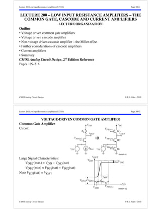
VOLTAGE-DRIVEN COMMON GATE AMPLIFIER
Common Gate Amplifier
Circuit:
Large Signal Characteristics:
vIN
RL
VNBias2
VOUT(max) VDD – VDS3(sat)
VOUT(min) VDS1(sat) + VDS2(sat)
Note VDS1(sat) = VON1
VDD
M3
vOUT
M2
M1
060609-01
VPBias1
VNBias2
VNBias1
VDD
vOUT
IBias vIN
vOUT
VDD VON3
vIN VNBias2
060609-02
VON1+VON2
VON1
VON2
VT2
CMOS Analog Circuit Design © P.E. Allen - 2010
- 2. Lecture 200 Low Input Resistance Amplifiers (3/27/10) Page 200-3
Small Signal Performance of the Common Gate Amplifier
Small signal model:
Rin
Rout Rin i1
vin rds1 vout
060609-03
rds2
gm2vgs2
−v
Rout
vin rds1 vout
gs2
+
rds3
rds2
gm2vs2
+
vs2
−
rds3
vout = gm2vs2
rds2
rds2+rds3 rds3 =
gm2rds2rds3
rds2+rds3 vin Av=
vout
vin =+
gm2rds2rds3
rds2+rds3
Rin = Rin’||rds1, Rin’ is found as follows
vs2 = (i1 - gm2vs2)rds2 + i1rds3 = i1(rds2 + rds3) - gm2 rds2vs2
Rin' =
vs2
i1 =
rds2+rds3
1+gm2rds2
Rin=rds1||
rds2+rds3
1+gm2rds2
Routrds2||rds3
CMOS Analog Circuit Design © P.E. Allen - 2010
Lecture 200 Low Input Resistance Amplifiers (3/27/10) Page 200-4
Influence of the Load on the Input Resistance of a Common Gate Amplifier
Consider a common gate amplifier with a general load:
VDD
VNBias2
VNBias1
vOUT
Load
M2
vIN M1
VDD
VNBias2
Rin1 Rin2
VNBias1
vOUT
M2
vIN M1
VDD
VPBias1
VNBias2
VNBias1
vOUT
M3
M2
vIN M1
V VDD PBias1
vOUT
M4
M3
M2
VPBias2
Rin3
vIN M1
070420-01
VNBias2
VNBias1
From the previous page, the input resistance to the common gate configuration is,
Rin =
rds2+RLoad
1+gm2rds2
For the various loads shown, Rin becomes:
rds2
Rin1 =
1+gm2rds2
1
gm2
Rin2 =
rds2+rds3
1+gm2rds2
2
gm2
Rin3 =
rds2+rds4gm3rds3
1+gm2rds2
rds!!!
The input resistance of the common gate configuration depends on the load at the drain
CMOS Analog Circuit Design © P.E. Allen - 2010
- 3. Lecture 200 Low Input Resistance Amplifiers (3/27/10) Page 200-5
Frequency Response of the Common Gate Amplifier
Circuit:
Vin rds1 Vout Cout
060609-04
VDD
VPBias1
Cbd3
Cgd3
Cgd2 Cbd2
VNBias2
VNBias1
vOUT
M3
M2
vIN M1
+
rds2
CL gm2Vs2
Vs2
−
rds3
The frequency response can be found by replacing rds3 in the previous slide with,
rds3
rds3
srds3Cout+1 where Cout = Cgd2 + Cgd3 + Cbd2 + Cbd3 + CL
Av(s) =
Vout
Vin = +
gm2rds2rds3
rds2+rds3
1
rds2rds3Cout
rds2+rds3 +1
s
gm2rds2rds3
rds2+rds3
= +
s
p1
1
1-
where p1 =
-1
rds2rds3Cout
rds2+rds3
-3dB = |p1|
CMOS Analog Circuit Design © P.E. Allen - 2010
Lecture 200 Low Input Resistance Amplifiers (3/27/10) Page 200-6
VOLTAGE-DRIVEN CASCODE AMPLIFIER
Cascode† Amplifier
VDD
M3
vOUT
M2
M1
060609-05
VPBias1
VNBias2
vIN
Advantages of the cascode amplifier:
• Increases the output resistance and gain (if M3 is cascaded also)
• Eliminates the Miller effect when the input source resistance is large
† “Cascode” = “Cascaded triode” see H. Wallman, A.B. Macnee, and C.P. Gadsden, “A Low-Noise Amplifier, Proc. IRE, vol. 36, pp. 700-708, June
1948.
CMOS Analog Circuit Design © P.E. Allen - 2010
- 4. Lecture 200 Low Input Resistance Amplifiers (3/27/10) Page 200-7
Large-Signal Characteristics of the Cascode Amplifier
M3
K
J
vIN=5.0V
vIN=4.5V
G F
IH E
0.5
0.4
0.3
0.2
0.1
0.0
D
A,B
0 1 2 3 4 5
ID (mA)
vOUT
M3
M2
M1
+
vIN
5V
W3
L3
ID
=2μm
1μm
+
W2
L2
= 2μm
1μm
vOUT
-
W1
L1
-
= 2μm
1μm
vIN=4.0V
vIN=3.5V
vIN=3.0V
vIN=2.5V
vIN=2.0V
vIN=1.5V
C
2.3V
vIN=1.0V
A B C
3.4V
D
E
M2 saturated
M2 active
G H
I K
F
J
5
4
3
2
1
0
M3 active
M3 saturated
M1 sat-urated
M1
active
0 1 2 3 4 5
vOUT
vIN
Fig. 5.3-2
M1 sat. when VGG2-VGS2 VGS1-VT vIN 0.5(VGG2+VTN) where VGS1=VGS2
M2 sat. when VDS2VGS2-VTN vOUT-VDS1VGG2-VDS1-VTN vOUT VGG2-VTN
M3 is saturated when VDD-vOUT VDD - VGG3 - |VTP| vOUT VGG3 + |VTP|
CMOS Analog Circuit Design © P.E. Allen - 2010
Lecture 200 Low Input Resistance Amplifiers (3/27/10) Page 200-8
Large-Signal Voltage Swing Limits of the Cascode Amplifier
Maximum output voltage, vOUT(max):
vOUT(max)=VDD
Minimum output voltage, vOUT(min):
Referencing all potentials to the negative power supply (ground in this case), we may
express the current through each of the devices, M1 through M3, as
iD1 = 1
2
2 1(VDD - VT1)vDS1
vDS1
(VDD-VT1)vDS1-
iD2 = 2
(VGG2-vDS1-VT2)(vOUT-vDS1)-
(vOUT-vDS1)2
2
2(VGG2 - vDS1 - VT2)(vOUT - vDS1)
and
iD3 =
3
2
(VDD VGG3 |VT3|)2
where we have also assumed that both vDS1 and vOUT are small, and vIN = VDD.
Solving for vOUT by realizing that iD1 = iD2 = iD3 and 1 = 2 we get,
3
22(VDDVGG3|VT3|)2
vOUT(min)=
1
VGG2VT2+
1
VDDVT1
CMOS Analog Circuit Design © P.E. Allen - 2010
- 5. Lecture 200 Low Input Resistance Amplifiers (3/27/10) Page 200-9
Small-Signal Midband Performance of the Cascode Amplifier
Small-signal model:
G1 D1=S2 D2=D3
gm1vgs1 rds1
+
vin =
vgs1
-
+
vout
rds2
gm2vgs2= -gm2v1
rds3
-
+
v1
-
S1=G2=G3
Small-signal model of cascode amplifier neglecting the bulk effect on M2.
C1
G1 D1=S2 D2=D3
gm1vin rds1
+
vin
-
+
vout
rds2
C2 gm2v1 rds3
C3
-
+
v1
-
1
gm2
Simplified equivalent model of the above circuit. Fig. 5.3-3
Using nodal analysis, we can write,
[gds1 + gds2 + gm2]v1 gds2vout = gm1vin
[gds2 + gm2]v1 + (gds2 + gds3)vout = 0
Solving for vout/vin yields
vout
vin =
gm1(gds2+gm2)
gds1gds2+gds1gds3+gds2gds3+gds3gm2
gm1
gds3 =
2K'1W1
L1ID23
(Intuitive analysis give the same result with much less effort.)
The small-signal output resistance is,
rout = [rds1 + rds2 + gm2rds1rds2]||rds3 rds3
CMOS Analog Circuit Design © P.E. Allen - 2010
Lecture 200 Low Input Resistance Amplifiers (3/27/10) Page 200-10
Frequency Response of the Cascode Amplifier
Small-signal model (RS = 0):
where
C1
C1 = Cgd1,
C2 = Cbd1+Cbs2+Cgs2, and
C3 = Cbd2+Cbd3+Cgd2+Cgd3+CL
The nodal equations now become:
G1 D1=S2 D2=D3
gm1vin rds1
+
vin
-
rds2
+
v1
C2 gm2v1 C3
-
1
gm2
(gm2 + gds1 + gds2 + sC1 + sC2)v1 gds2vout = (gm1 sC1)vin
and (gds2 + gm2)v1 + (gds2 + gds3 + sC3)vout = 0
Solving for Vout(s)/Vin(s) gives,
Vout(s)
Vin(s) =
1
1+as+bs2
(gm1sC1)(gds2+gm2)
gds1gds2+gds3(gm2+gds1+gds2)
where
a =
C3(gds1+gds2+gm2)+C2(gds2+gds3)+C1(gds2+gds3)
gds1gds2+gds3(gm2+gds1+gds2)
and
b =
C3(C1+C2)
gds1gds2+gds3(gm2+gds1+gds2)
+
vou
rds3
-
Fig. 5.3-4A
CMOS Analog Circuit Design © P.E. Allen - 2010
- 6. Lecture 200 Low Input Resistance Amplifiers (3/27/10) Page 200-11
A Simplified Method of Finding an Algebraic Expression for the Two Poles
Assume that a general second-order polynomial can be written as:
P(s) = 1 + as + bs2 =
1
s
p1
s
p2 = 1 s
1
1
p2 +
1
p1+
s2
p1p2
Now if |p2| |p1|, then P(s) can be simplified as
P(s) 1
s
p1 +
s2
p1p2
Therefore we may write p1 and p2 in terms of a and b as
p1 =
1
a and p2 =
a
b
Applying this to the previous problem gives,
p1 =
[gds1gds2+gds3(gm2+gds1+gds2)]
C3(gds1+gds2+gm2)+C2(gds2+gds3)+C1(gds2+gds3)
gds3
C3
The nondominant root p2 is given as
p2 =
[C3(gds1+gds2+gm2)+C2(gds2+gds3)+C1(gds2+gds3)]
C3(C1+C2)
gm2
C1+C2
Assuming C1, C2, and C3 are the same order of magnitude, and gm2 is greater than gds3,
then |p1| is smaller than |p2|. Therefore the approximation of |p2| |p1| is valid.
Note that there is a right-half plane zero at z1 = gm1/C1.
CMOS Analog Circuit Design © P.E. Allen - 2010
Lecture 200 Low Input Resistance Amplifiers (3/27/10) Page 200-12
NON-VOLTAGE DRIVEN CASCODE AMPLIFIER – THE MILLER EFFECT
Miller Effect
Consider the following inverting amplifier:
Solve for the input impedance:
Zin(s) =
V1
I1
I1
+
V1
−
CM
-Av
I1 = sCM(V1 – V2) = sCM(V1 + AvV1) = sCM(1 + Av)V1
Therefore,
Zin(s) =
V1
I1 =
V1
sCM(1+Av)V1 =
1
sCM(1+Av) =
1
sCeq
+
V2 = -AvV1
−
060610-03
The Miller effect can take Cgd = 5fF and make it look like a 0.5pF capacitor in parallel
with the input of the inverting amplifier (Av -100).
If the source resistance is large, this creates a dominant pole at the input.
CMOS Analog Circuit Design © P.E. Allen - 2010
- 7. Lecture 200 Low Input Resistance Amplifiers (3/27/10) Page 200-13
Simple Inverting Amplifier Driven with a High Source Resistance
Examine the frequency
response of a current-source load
inverter driven from a high
resistance source:
Assuming the input is Iin, the
VGG2
vin Rs
VDD
vout
M2
M1
Rs
Vin
R Rs s
C1
C2
C3 R3
C1 ≈ Cgs1
C2 = Cgd1
gm1V1
C3 = Cbd1 + Cbd2 + Cgd2
R3 = rds1||rds2 Fig.
+
V1
-
nodal equations are,
[G1 + s(C1 + C2)]V1 sC2Vout = Iin and (gm1sC2)V1+[G3+s(C2+C3)]Vout = 0
where
G1 = Gs (=1/Rs), G3 = gds1 + gds2, C1 = Cgs1, C2 = Cgd1 and C3 = Cbd1+Cbd2 + Cgd2.
Solving for Vout(s)/Vin(s) gives
Vout(s)
(sC2gm1)G1
Vin(s) =
G1G3+s[G3(C1+C2)+G1(C2+C3)+gm1C2]+(C1C2+C1C3+C2C3)s2 or,
Vout(s)
Vin(s) =
gm1
G3
[1s(C2/gm1)]
1+[R1(C1+C2)+R3(C2+C3)+gm1R1R3C2]s+(C1C2+C1C3+C2C3)R1R3s2
Assuming that the poles are split allows the use of the previous technique to get,
1
p1 =
R1(C1+C2)+R3(C2+C3)+gm1R1R3C2
1
gm1R1R3C2 andp2
gm1C2
C1C2+C1C3+C2C3
The Miller effect has caused the input pole, 1/R1C1, to be decreased by a value of gm1R3.
CMOS Analog Circuit Design © P.E. Allen - 2010
Lecture 200 Low Input Resistance Amplifiers (3/27/10) Page 200-14
How Does the Cascode Amplifier Solve the Miller Effect?
Cascode amplifier:
+
vOUT
−
060610-02
VPBias1
VNBias2
+
vIN
-
VDD
M3
M2
Cgd1
M1
Rs2
+
v1
−
RS
vS
The Miller effect causes Cgs1 to be increased by the value of 1 + (v1/vin) and appear in
parallel with the gate-source of M1 causing a dominant pole to occur.
The cascode amplifier eliminates this problem by keeping the value of v1/vin small by
making the value of Rs2 approximately 2/gm2.
CMOS Analog Circuit Design © P.E. Allen - 2010
- 8. Lecture 200 Low Input Resistance Amplifiers (3/27/10) Page 200-15
Comparison of the Inverting and Cascode Non-Voltage Driven Amplifiers
The dominant pole of the inverting amplifier with a large source resistance was found to
be
p1(inverter) =
1
R1(C1+C2)+R3(C2+C3)+gm1R1R3C2
1
gm1R1R3C2
Now if a cascode amplifier is used, R3, can be approximated as 2/gm of the cascoding
transistor (assuming the drain sees an rds to ac ground).
p1(cascode) =
1
R1(C1+C2)+
2
gm
(C2+C3)+gm1R1
2
gm
C2
=
1
R1(C1+C2)+
2
gm
(C2+C3)+2R1C2
1
R1(C1+3C2)
Thus we see that p1(cascode) p1(inverter).
CMOS Analog Circuit Design © P.E. Allen - 2010
Lecture 200 Low Input Resistance Amplifiers (3/27/10) Page 200-16
FURTHER CONSIDERATIONS OF CASCODE AMPLIFIERS
High Gain and High Output Resistance Cascode Amplifier
If the load of the cascode
amplifier is a cascode
current source, then both
high output resistance
and high voltage gain is
achieved.
The output resistance is,
VDD
VPBias1
VPBias2
VNBias2
vin
Rout
M4
M3
M2
M1
rout [gm2rds1rds2][gm3rds3rds4] =
D2=D3
gm2v1 gmbs2v1 rds2 gm3v4 gmbs3v4 rds3
G1 D1=S2 D4=S3
gm1vin
I
-1.5
D
vout
+
vin
-
12
2K'2(W/L)2
+
+
+
v4
v1 rds1
rds4
-
G2=G3=G4=S1=S4
34
2K'3(W/L)3
Knowing rout, the gain is simply
Av = gm1rout gm1{[gm2rds1rds2][gm3rds3rds4]}
-
2K'1(W/L)1I
-1
D
12
2K'2(W/L)2
+
+
vout
-
060609-07
34
2K'3(W/L)3
CMOS Analog Circuit Design © P.E. Allen - 2010
- 9. Lecture 200 Low Input Resistance Amplifiers (3/27/10) Page 200-17
Example 200-1 - Comparison of the Cascode Amplifier Performance
Calculate the small-signal voltage gain, output resistance, the dominant pole, and the
nondominant pole for the low-gain, cascode amplifier and the high-gain, cascode
amplifier. Assume that ID = 200 microamperes, that all W/L ratios are 2μm/1μm, and
that the parameters of Table 3.1-2 are valid. The capacitors are assumed to be: Cgd = 3.5
fF, Cgs = 30 fF, Cbsn = Cbdn = 24 fF, Cbsp = Cbdp = 12 fF, and CL = 1 pF.
Solution
The low-gain, cascode amplifier has the following small-signal performance:
Av = 37.1V/V
Rout = 125k
p1 -gds3/C3 1.22 MHz
p2 gm2/(C1+C2) 605 MHz.
The high-gain, cascode amplifier has the following small-signal performance:
Av = 414V/V
Rout = 1.40 M
p1 1/RoutC3 108 kHz
p2 gm2/(C1+C2) 579 MHz
(Note at this frequency, the drain of M2 is shorted to ground by the load capacitance, CL)
CMOS Analog Circuit Design © P.E. Allen - 2010
Lecture 200 Low Input Resistance Amplifiers (3/27/10) Page 200-18
Designing Cascode Amplifiers
Pertinent design equations for the simple cascode amplifier.
+
vIN
-
vOUT(max) = VDD - VSD3(sat)
+
=VDD -
vOUT
-
VDD
M3
M2
I
M1
(VDD - VGG3-|VTP|)2
VGG3
VGG2
KPW3
2L3
VGG2 = VDS1(sat) + VGS2
Fig. 5.3-7
2I
KP(W3/L3)
vOUT(min) =VDS1(sat) + VDS2(sat)
2I
= +
KN(W1/L1)
2I
KN(W2/L2)
I = Pdiss
VDD
= (SR)·Cout
|Av| =
gm1
gds3
= 2KN(W1/L1)
2I
λP
I =
CMOS Analog Circuit Design © P.E. Allen - 2010
- 10. Lecture 200 Low Input Resistance Amplifiers (3/27/10) Page 200-19
Example 200-2 - Design of a Cascode Amplifier
The specs for a cascode amplifier are Av = -50V/V, vOUT(max) = 4V, vOUT(min) = 1.5V,
VDD=5V, and Pdiss=1mW. The slew rate with a 10pF load should be 10V/μs or greater.
Solution
The slew rate requires a current greater than 100μA while the power dissipation
requires a current less than 200μA. Compromise with 150μA. Beginning with M3,
W3
L3
=
2I
KP[VDD-vOUT(max)]2 =
2·150
50(1)2 = 6
From this find VGG3: VGG3 = VDD - |VTP| -
2I
KP(W3/L3) = 5 - 1 -
2·150
50·6 = 3V
Next,
W1
L1
=
(Av)2I
2KN
=
(50·0.05)2(150)
2·110 = 2.73
To design W2/L2, we will first calculate VDS1(sat) and use the vOUT(min) specification to
2I
define VDS2(sat). VDS1(sat) =
KN(W1/L1) =
2·150
110·4.26 = 0.8V
Subtracting this value from 1.5V gives VDS2(sat) = 0.7V.
W2
L2
=
2I
KNVDS2(sat)2 =
2·150
110·0.72 = 5.57
Finally, VGG2 = VDS1(sat) +
2I
KN(W2/L2) + VTN = 0.8V+ 0.7V + 0.7V = 2.2V
CMOS Analog Circuit Design © P.E. Allen - 2010
Lecture 200 Low Input Resistance Amplifiers (3/27/10) Page 200-20
CURRENT AMPLIFIERS
What is a Current Amplifier?
• An amplifier that has a defined output-input current relationship
• Low input resistance
• High output resistance
Application of current amplifiers:
ii io
Ai iS RS
Current
Amplifier
iS RS RL
RL
ii
io
+
ii Ai
Current
Amplifier
-
Single-ended input. Differential input. Fig. 5.4-1
RS Rin and Rout RL
Advantages of current amplifiers:
• Currents are not restricted by the power supply voltages so that wider dynamic
ranges are possible with lower power supply voltages.
• -3dB bandwidth of a current amplifier using negative feedback is independent of the
closed loop gain.
CMOS Analog Circuit Design © P.E. Allen - 2010
- 11. Lecture 200 Low Input Resistance Amplifiers (3/27/10) Page 200-21
Frequency Response of a Current Amplifier with Current Feedback
Consider the following current amplifier with resistive
negative feedback applied.
Assuming that the small-signal resistance looking into
the current amplifier is much less than R1 or R2,
io = Ai(i1-i2) = Ai
vin
R1
-io
Solving for io gives
io =
Ai
1+Ai
vin
R1
vout = R2io =
R2
R1
Ai
1+Ai
vin
If Ai(s) =
Ao
s
A+1
, then
vout
vin
=
R2
R1
1
Ai(s)
1
1+
=
R2
R1
Ao
s
A
+(1+Ao)
=
R2
R1
Ao
1+Ao
vin
i R2 2
-
+
i1 Ai
R1 vout
1
s
A(1+Ao)+1
-3dB = A(1+Ao)
io
Fig. 5.4-2
CMOS Analog Circuit Design © P.E. Allen - 2010
Lecture 200 Low Input Resistance Amplifiers (3/27/10) Page 200-22
Bandwidth Advantage of a Current Feedback Amplifier
The unity-gainbandwidth is,
GB = |Av(0)| -3dB =
R2Ao
R1(1+Ao) · A(1+Ao) =
R2
R1
Ao·A =
R2
R1
GBi
where GBi is the unity-gainbandwidth of the current amplifier.
Note that if GBi is constant, then increasing R2/R1 (the voltage gain) increases GB.
Illustration:
Magnitude dB
Ao dB
1+Ao
Ao dB K
1+Ao
Ao dB
Voltage Amplifier, R2 K
R2
R1
Voltage Amplifier,
= K
Current Amplifier
ωA
R1
1
R2
R1
GB1 GB2
0dB
log10(ω)
Fig. 7.2-10
(1+Ao)ωA
GBi
Note that GB2 GB1 GBi
The above illustration assumes that the GB of the voltage amplifier realizing the voltage
buffer is greater than the GB achieved from the above method.
CMOS Analog Circuit Design © P.E. Allen - 2010
- 12. Lecture 200 Low Input Resistance Amplifiers (3/27/10) Page 200-23
Current Amplifier using the Simple Current Mirror
VDD VDD
I1 I i 2 in iout
R
M1 M2
Current Amplifier
iin iout
vin
gm1vin
+
-
C2
rds1 C1 gm2vin rds2 C3
RL
≈ 0
Fig. 5.4-3
Rin =
1
gm1
Rout =
1
1Io
and Ai =
W2/L2
W1/L1
.
Frequency response:
p1 =
-(gm1+gds1)
C1+C2
=
-(gm1+gds1)
Cbd1+Cgs1+Cgs2+Cgd2
-gm1
Cbd1+Cgs1+Cgs2+Cgd2
Note that the bandwidth can be almost doubled by including the resistor, R.
(R removes Cgs1 from p1)
CMOS Analog Circuit Design © P.E. Allen - 2010
Lecture 200 Low Input Resistance Amplifiers (3/27/10) Page 200-24
Example 200-3 - Performance of a Simple Current Mirror as a Current Amplifier
Find the small-signal current gain, Ai, the input resistance, Rin, the output resistance
Rout, and the -3dB frequency in Hertz for the current amplifier of previous slide if 10I1 = I2
= 100μA and W2/L2 = 10W1/L1 = 10μm/1μm. Assume that Cbd1 = 10fF, Cgs1 = Cgs2 =
100fF, and Cgs2 = 50fF.
Solution
Ignoring channel modulation and mismatch effects, the small-signal current gain,
Ai =
W2/L2
W1/L1
10A/A.
The small-signal input resistance, Rin, is approximately 1/gm1 and is
Rin
1
2KN(1/1)10μA =
1
46.9μS = 21.3k
The small-signal output resistance is equal to
Rout =
1
NI2
= 250k.
The -3dB frequency is
-3dB =
46.9μS
260fF = 180.4x10⁶ radians/sec. f-3dB = 28.7 MHz
CMOS Analog Circuit Design © P.E. Allen - 2010
- 13. Lecture 200 Low Input Resistance Amplifiers (3/27/10) Page 200-25
Wide-Swing, Cascode Current Mirror Implementation of a Current Amplifier
+
VDD
iout
M4
VDD
M3
IIN
IOUT
VNBias2
M1 M2
vOUT
−
060610-01
+
iin
vIN
−
Rin
1
gm1
, Rout rds2gm4rds4, and Ai =
W2/L2
W1/L1
CMOS Analog Circuit Design © P.E. Allen - 2010
Lecture 200 Low Input Resistance Amplifiers (3/27/10) Page 200-26
Example 200-4 - Current Amplifier Implemented by the Wide-Swing, Cascode
Current Mirror
Assume that IIN and IOUT of the wide-swing cascode current mirror are 100μA.
Find the value of Rin, Rout, and Ai if the W/L ratios of all transistors are 182μm/1μm.
Solution
The input resistance requires gm1 which is 2·110·182·100 = 2mS
Rin 500
From our knowledge of the cascode configuration, the small signal output resistance
should be
Rout gm4rds4rds2 = (2001μS)(250k)(250k) = 125M
Because VDS1 = VDS2, the small-signal current gain is
Ai =
W2/L2
W1/L1 = 1
Simulation results using the level 1 model for this example give
Rin= 497, Rout = 164.7M and Ai = 1.000 A/A.
The value of VON for all transistors is
VON =
2·100μA
110μA/V2·182 = 0.1V
CMOS Analog Circuit Design © P.E. Allen - 2010
- 14. Lecture 200 Low Input Resistance Amplifiers (3/27/10) Page 200-27
Low-Input Resistance Current Amplifier
To decrease Rin below 1/gm
requires the use of negative,
shunt feedback. Consider
the following example.
Feedback concept:
i I1 I2 iout in
M1
VDD VDD
M3
I3
Current Amplifier
Input resistance without feedback rds1.
Loop gain
gm1
gds1
gm3
gds3
VGG3
M2
iin
gm1vgs1 rds1
i = 0
gm3vgs3 +
rds3
vgs1
-
-
vgs3
+
+
vin
-
Fig. 5.4-5
assuming that the resistances of I1 and I3 are very large.
Rin =
Rin(nofb.)
1+Loopgain
rds1
gm1rds1gm3rds3
=
1
gm1gm3rds3
Small signal analysis:
iin = gm1vgs1 - gds1vgs3
and vgs3 = -vin vgs1 = vin - (gm3 vgs3rds3) = vin(1+gm3rds3)
iin = gm1(1+gm3rds3)vin + gds1vin gm1gm3rds3vin Rin
1
gm1gm3rds3
CMOS Analog Circuit Design © P.E. Allen - 2010
Lecture 200 Low Input Resistance Amplifiers (3/27/10) Page 200-28
Use of Blackman’s Formula to Find the Input Resistance of Previous Slide
Recall that the resistance seen looking into port X is given as,
Rx = Rx(k=0)
1+RR(portshorted)
1+RR(portopened)
The small signal circuit (from the previous slide) is,
Choosing gm1 as k, we see that,
Rx(k=0) = rds1
The circuits for calculating the shorted and open return-ratios are:
vc
vc' = 0 RR(ix = 0): vc = - vgs3(1+ gm3rds3) = - gm1rds1 (1+ gm3rds3)vc’
RR(vx = 0): -
RR(ix = 0) = -
vc
vc' = gm1rds1 (1+ gm3rds3)
Finally,
Rx = Rin = rds1
1+0
1+gm1rds1(1+gm3rds3)
1
gm1gm3rds3
CMOS Analog Circuit Design © P.E. Allen - 2010
- 15. Lecture 200 Low Input Resistance Amplifiers (3/27/10) Page 200-29
Differential-Input, Current Amplifiers
Definitions for the differential-mode, iID, and common-mode, iIC, input currents of the
differential-input current amplifier.
+
-
i1
i2
iID
iIC
2
iIC
2
iO
Fig. 5.4-6
iO = AIDiID ± AICiIC = AID(i1 - i2) ± AIC
i1+i2
2
Implementations:
VDD VDD VDD
I 2I I
i1
i2 i2
iO
i1-i2
M1 M2 M3 M4
iO
VDD
M3 M4
M1 M2
i1 i2
VGG1
M5 M6
VGG2
Fig. 5.4-7
CMOS Analog Circuit Design © P.E. Allen - 2010
Lecture 200 Low Input Resistance Amplifiers (3/27/10) Page 200-30
SUMMARY
• Low input resistance amplifiers use the source as the input terminal with the gate
generally on ground
• The input resistance to the common gate amplifier depends on what is connected to the
drain
• The voltage driven common gate/common source amplifier has one dominant pole
• The current driven common gate/common source amplifier has two dominant poles
• The cascode amplifier eliminates the input dominant pole for the current driven common
gate/common source amplifier
• Current amplifiers have a low input resistance, high output resistance, and a defined
output-input current relationship
• Input resistances less than 1/gm require feedback
However, all feedback loops have internal poles that cause the benefits of negative
feedback to vanish at high frequencies.
In addition, feedback loops can have a slow time constant from a pole-zero pair.
• Voltage amplifiers using a current amplifier have high values of gain-bandwidth
• Current amplifiers are useful at low power supplies and for switched current
applications
CMOS Analog Circuit Design © P.E. Allen - 2010