Downloaded 177 times

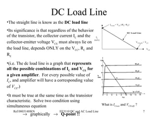
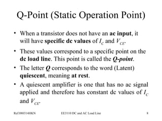

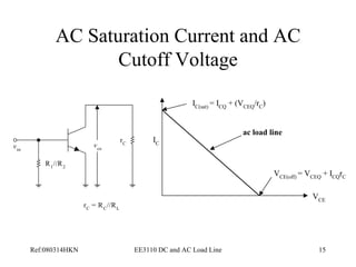
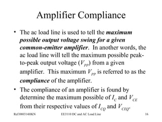
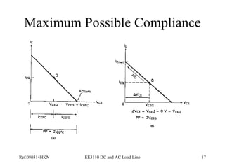
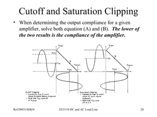
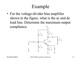

The document discusses DC and AC analysis of transistor amplifiers. It covers DC biasing circuits, voltage divider bias, graphical DC analysis using load lines and Q-point, AC equivalent circuits, and determining amplifier compliance from the AC load line. Key points are: - DC load line shows all combinations of collector current (IC) and collector-emitter voltage (VCE) for given values of voltage and resistors. - Q-point is the operating point where the load line intersects the transistor characteristic curve with no input signal. - AC load line determines maximum output voltage compliance or swing based on saturation and cutoff points.