Download as PDF, PPTX
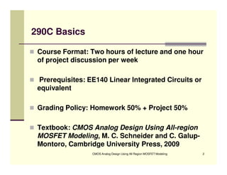


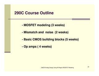
EE 290C is a course on CMOS analog design using all-region MOSFET modeling taught by Carlos Galup-Montoro. [1] The course format includes two hours of lecture and one hour of project discussion per week. [2] Prerequisites for the course are EE140 Linear Integrated Circuits or equivalent, and grading is based on homework assignments and a project. [3] The course aims to provide an understanding of MOSFET modeling and application to the design of basic CMOS building blocks and operational amplifiers.


