Downloaded 975 times
![Introduction to the course Name: “ Analog VLSI Design ” Instructor: Nguyen Cao Qui email: [email_address] Goals: The goal of this course is to introduce the principles of operation, design and technology of Analog Integrated Circuits to Electrical Engineering students at Senior level. VLSI technology and analog integrated circuit design is covered with an emphasis on CMOS Technology. CMOS layout design and analog simulation tools (Microwind) are demonstrated and used. Students will do a design project and final exam at the end.](https://image.slidesharecdn.com/analogvlsi-110427212224-phpapp02/85/Analog-vlsi-2-320.jpg)
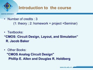


This document provides an overview of an "Analog VLSI Design" course. The goals of the course are to introduce principles of analog integrated circuit design and CMOS technology. Students will learn about CMOS layout design using CAD tools and complete a design project. The course covers topics including CMOS technology, resistors, capacitors, MOSFETs, current mirrors, amplifiers, and data converters. Assessment includes homework, a project, and a final exam.